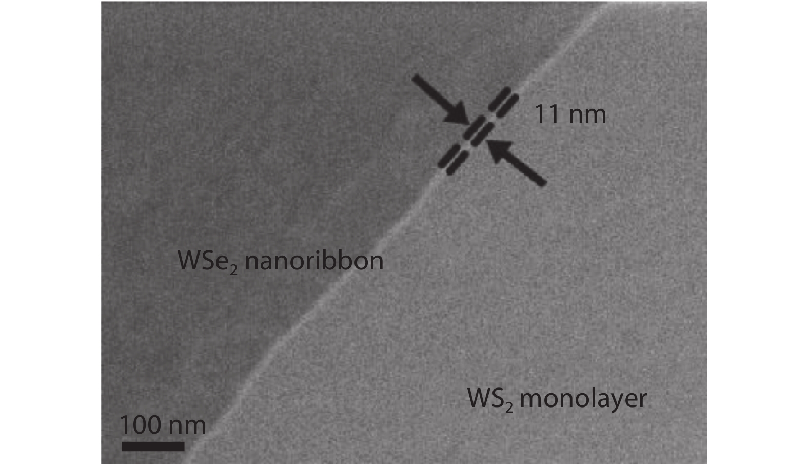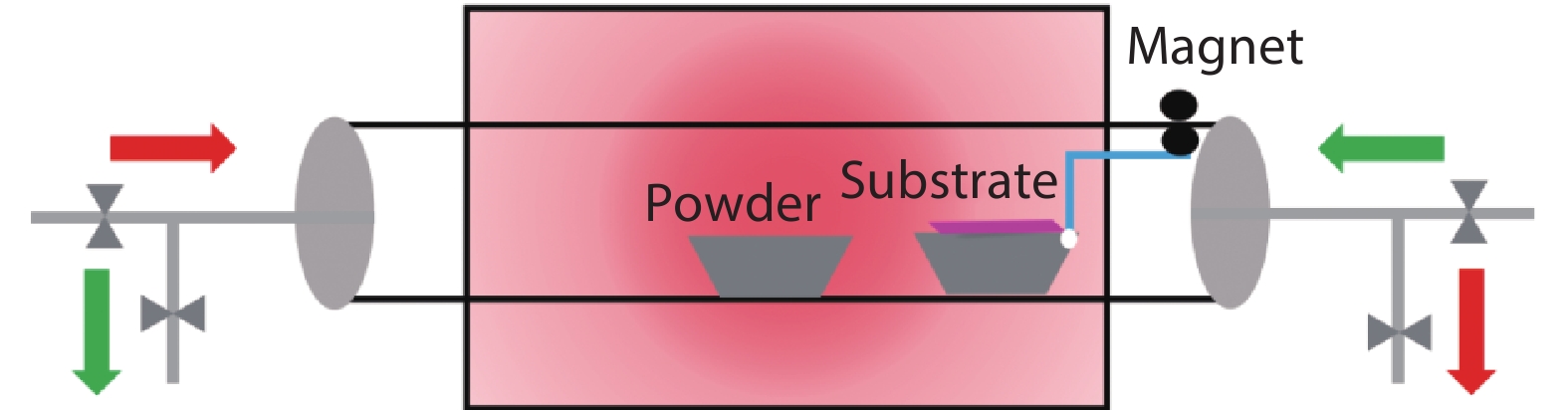
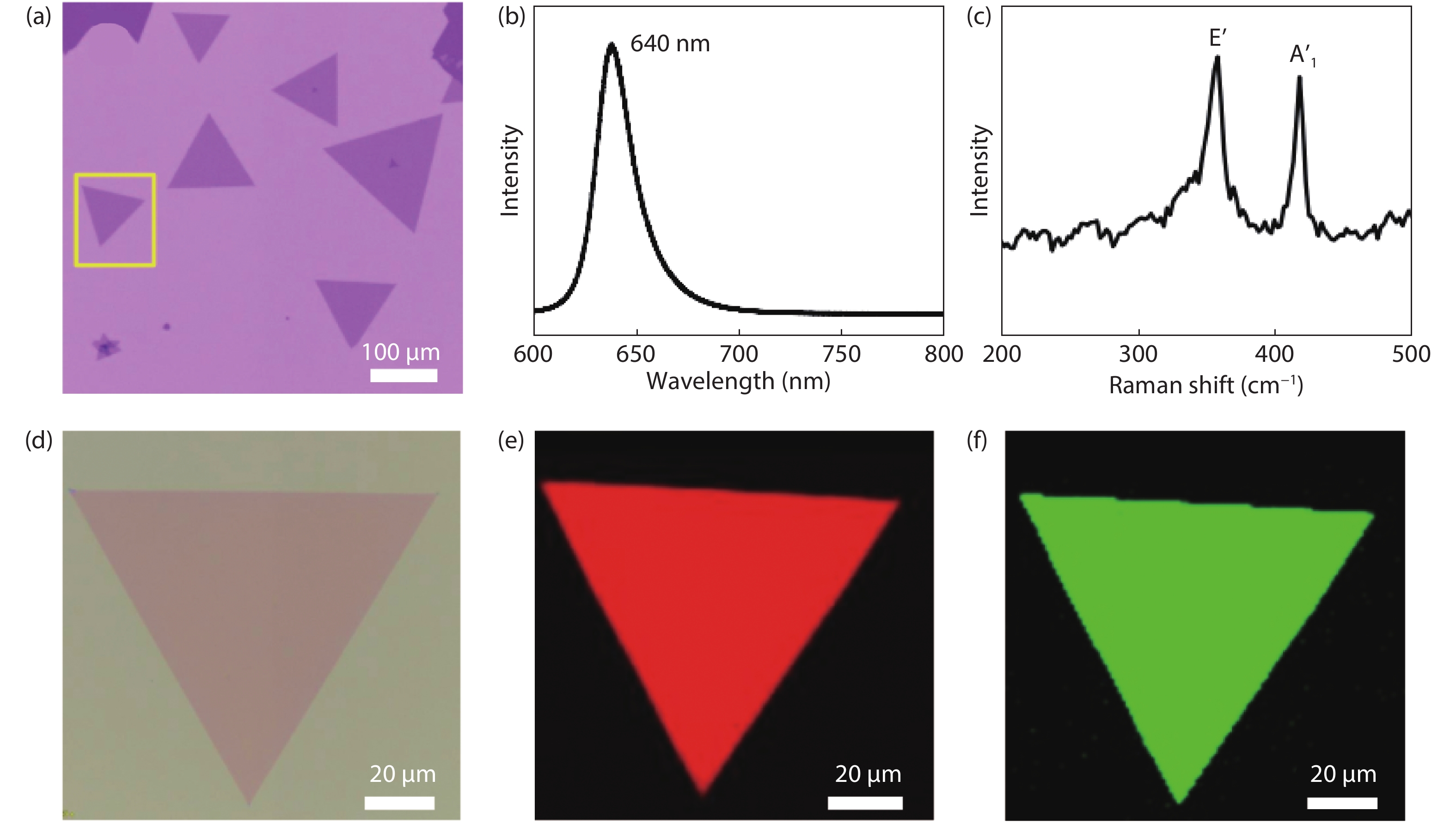
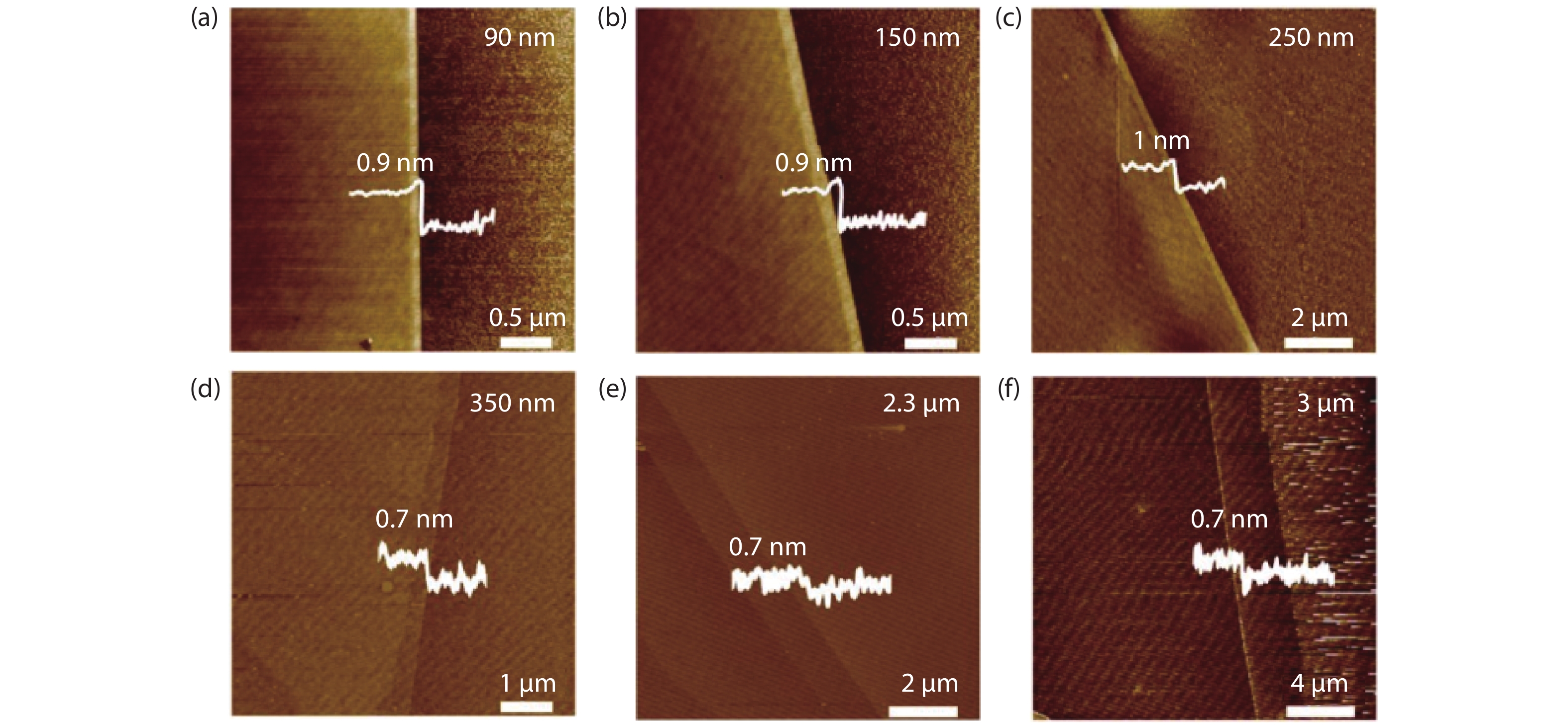
Fig. 1.
(Color online) Schematic of a modified bidirectional flow CVD system.
ARTICLES
Di Wang, Zucheng Zhang, Bo Li and Xidong Duan
Corresponding author: Xidong Duan, xidongduan@hnu.edu.cn
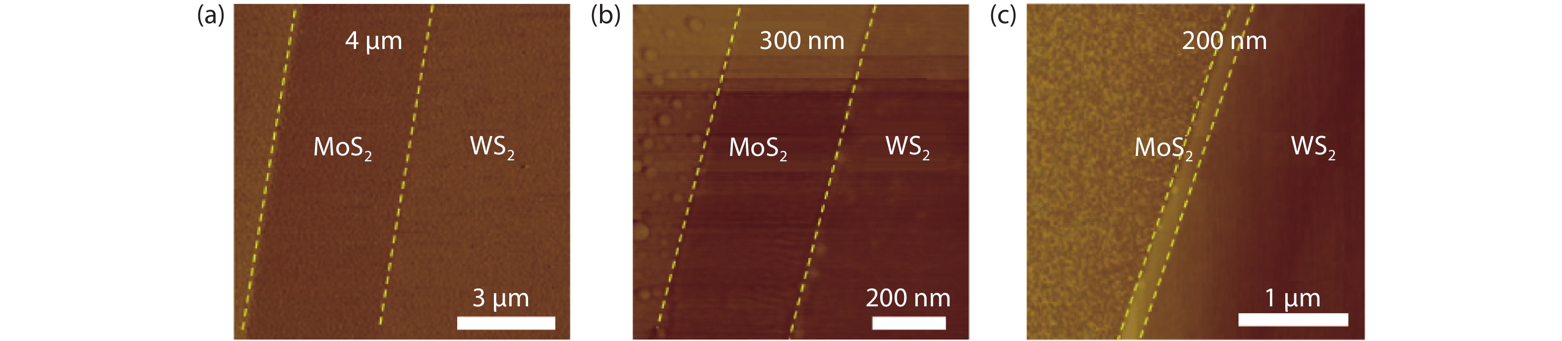
Abstract: Two-dimensional/one-dimensional (2D/1D) heterostructures as a new type of heterostructure have been studied for their unusual properties and promising applications in electronic and optoelectronic devices. However, the studies of 2D/1D heterostructures are mainly focused on vertical heterostructures, such as MoS2 nanosheet-carbon nanotubes. The research on lateral 2D/1D heterostructures with a tunable width of 1D material is still scarce. In this study, bidirectional flow chemical vapor deposition (CVD) was used to accurately control the width of the WS2/WSe2 (WS2/MoS2) heterostructures by controlling reacting time. WSe2 and MoS2 with different widths were epitaxially grown at the edge of WS2, respectively. Optical microscope, atomic force microscope (AFM), and scanning electron microscope (SEM) images show the morphology and width of the heterostructures. These results show that the width of the heterostructures can be as low as 10 nm by using this method. The interface of the heterostructure is clear and smooth, which is suitable for application. This report offers a new method for the growth of 1D nanowires, and lays the foundation for the future study of the physical and chemical properties of 2D/1D lateral heterostructures.
Key words: chemical vapor deposition (CVD), 2D/1D heterostructures, width control
| [1] |
Trentler T J, Hickman K M, Goel S C, et al. Solution-liquid-solid growth of crystalline III-V semiconductors: an analogy to vapor-liquid-solid growth. Science, 1995, 270(5243), 1791 doi: 10.1126/science.270.5243.1791
|
| [2] |
Yan R, Gargas D, Yang P. Nanowire photonics. Nat Photon, 2009, 3(10), 569 doi: 10.1038/nphoton.2009.184
|
| [3] |
Zheng L X, O'Connell M J, Doorn S K, et al. Ultralong single-wall carbon nanotubes. Nat Mater, 2004, 3(10), 673 doi: 10.1038/nmat1216
|
| [4] |
Lei S, Ge L, Najmaei S, et al. Evolution of the electronic band structure and efficient photo-detection in atomic layers of InSe. Acs Nano, 2014, 8(2), 1263 doi: 10.1021/nn405036u
|
| [5] |
Poh S M, Tan S J R, Zhao X, et al. Large area synthesis of 1D-MoSe2 using molecular beam epitaxy. Adv Mater, 2017, 29(12), 1605641 doi: 10.1002/adma.201605641
|
| [6] |
Qi R, Wang S, Wang M, et al. Towards well-defined MoS2 nanoribbons on a large scale. Chem Commun, 2017, 53(70), 9757 doi: 10.1039/C7CC04647B
|
| [7] |
Li S, Lin Y C, Zhao W, et al. Vapour-liquid-solid growth of monolayer MoS2 nanoribbons. Nat Mater, 2018, 17(6), 535 doi: 10.1038/s41563-018-0055-z
|
| [8] |
Huang W, Wang X, Ji X, et al. In-situ fabrication of Mo6S6-nanowire-terminated edges in monolayer molybdenum disulfide. Nano Res, 2018, 11(11), 5849 doi: 10.1007/s12274-018-2089-6
|
| [9] |
Zhou Y, Dong J, Li H, et al. Electronic transport properties of in-plane heterostructures constructed by MoS2 and WS2 nanoribbons. RSC Adv, 2015, 5(82), 66852 doi: 10.1039/C5RA14507D
|
| [10] |
Zhou W, Yu G, Rudenko A N, et al. Tunable half-metallicity and edge magnetism of H-saturated InSe nanoribbons. Phys Rev Mater, 2018, 2(11), 114001 doi: 10.1103/PhysRevMaterials.2.114001
|
| [11] |
Chen K X, Luo Z Y, Mo D C, et al. WSe2 nanoribbons: new high-performance thermoelectric materials. Phys Chem Chem Phys, 2016, 18(24), 16337 doi: 10.1039/C6CP02456D
|
| [12] |
Wu M, Shi J J, Zhang M, et al. Modulation of electronic and magnetic properties in InSe nanoribbons: edge effect. Nanotechnology, 2018, 29(20), 205708 doi: 10.1088/1361-6528/aab3f5
|
| [13] |
Magda G Z, Jin X, Hagymasi I, et al. Room-temperature magnetic order on zigzag edges of narrow graphene nanoribbons. Nature, 2014, 514(7524), 608 doi: 10.1038/nature13831
|
| [14] |
Wang J J, Cao F F, Jiang L, et al. High performance photodetectors of individual InSe single crystalline nanowire. J Am Chem Soc, 2009, 131(43), 15602 doi: 10.1021/ja9072386
|
| [15] |
Yu Y, Wang G, Tan Y, et al. Phase-controlled growth of one-dimensional Mo6Te6 nanowires and two-dimensional MoTe2 ultrathin films heterostructures. Nano Lett, 2018, 18(2), 675 doi: 10.1021/acs.nanolett.7b03058
|
| [16] |
Zhang J, Wei Y, Yao F, et al. SWCNT-MoS2-SWCNT vertical point heterostructures. Adv Mater, 2017, 29(7), 1604469 doi: 10.1002/adma.201604469
|
| [17] |
Jariwala D, Sangwan V K, Wu C C, et al. Gate-tunable carbon nanotube-MoS2 heterojunction p-n diode. Proc Natl Acad Sci USA, 2013, 110(45), 18076 doi: 10.1073/pnas.1317226110
|
| [18] |
Liu Y, He X, Hanlon D, et al. Liquid phase exfoliated MoS2 nanosheets percolated with carbon nanotubes for high volumetric/areal capacity sodium-ion batteries. Acs Nano, 2016, 10(9), 8821 doi: 10.1021/acsnano.6b04577
|
| [19] |
Huang H, Huang W, Yang Z, et al. Strongly coupled MoS2 nanoflake-carbon nanotube nanocomposite as an excellent electrocatalyst for hydrogen evolution reaction. J Mater Chem A, 2017, 5(4), 1558 doi: 10.1039/C6TA09612C
|
| [20] |
Zhang Z, Chen P, Duan X, et al. Robust epitaxial growth of two-dimensional heterostructures, multiheterostructures, and superlattices. Science, 2017, 357(6353), 788 doi: 10.1126/science.aan6814
|
| [21] |
Duan X, Wang C, Shaw J C, et al. Lateral epitaxial growth of two-dimensional layered semiconductor heterojunctions. Nat Nanotechnol, 2014, 9(12), 1024 doi: 10.1038/nnano.2014.222
|
| [22] |
Berkdemir A, Gutierrez H R, Botello-Mendez A R, et al. Identification of individual and few layers of WS2 using Raman Spectroscopy. Sci Rep, 2013, 3, 1755 doi: 10.1038/srep01755
|
| [23] |
van der Zande A M, Huang P Y, Chenet D A, et al. Grains and grain boundaries in highly crystalline monolayer molybdenum disulphide. Nat Mater, 2013, 12, 554 doi: 10.1038/nmat3633
|


Article views: 2827 Times PDF downloads: 93 Times Cited by: 0 Times
Received: 07 April 2021 Revised: 21 April 2021 Online: Accepted Manuscript: 31 May 2021Uncorrected proof: 29 June 2021Published: 01 September 2021
| Citation: |
Di Wang, Zucheng Zhang, Bo Li, Xidong Duan. Synthesis of two-dimensional/one-dimensional heterostructures with tunable width[J]. Journal of Semiconductors, 2021, 42(9): 092001. doi: 10.1088/1674-4926/42/9/092001
D Wang, Z C Zhang, B Li, X D Duan, Synthesis of two-dimensional/one-dimensional heterostructures with tunable width[J]. J. Semicond., 2021, 42(9): 092001. doi: 10.1088/1674-4926/42/9/092001.
Export: BibTex EndNote

|
| [1] |
Trentler T J, Hickman K M, Goel S C, et al. Solution-liquid-solid growth of crystalline III-V semiconductors: an analogy to vapor-liquid-solid growth. Science, 1995, 270(5243), 1791 doi: 10.1126/science.270.5243.1791
|
| [2] |
Yan R, Gargas D, Yang P. Nanowire photonics. Nat Photon, 2009, 3(10), 569 doi: 10.1038/nphoton.2009.184
|
| [3] |
Zheng L X, O'Connell M J, Doorn S K, et al. Ultralong single-wall carbon nanotubes. Nat Mater, 2004, 3(10), 673 doi: 10.1038/nmat1216
|
| [4] |
Lei S, Ge L, Najmaei S, et al. Evolution of the electronic band structure and efficient photo-detection in atomic layers of InSe. Acs Nano, 2014, 8(2), 1263 doi: 10.1021/nn405036u
|
| [5] |
Poh S M, Tan S J R, Zhao X, et al. Large area synthesis of 1D-MoSe2 using molecular beam epitaxy. Adv Mater, 2017, 29(12), 1605641 doi: 10.1002/adma.201605641
|
| [6] |
Qi R, Wang S, Wang M, et al. Towards well-defined MoS2 nanoribbons on a large scale. Chem Commun, 2017, 53(70), 9757 doi: 10.1039/C7CC04647B
|
| [7] |
Li S, Lin Y C, Zhao W, et al. Vapour-liquid-solid growth of monolayer MoS2 nanoribbons. Nat Mater, 2018, 17(6), 535 doi: 10.1038/s41563-018-0055-z
|
| [8] |
Huang W, Wang X, Ji X, et al. In-situ fabrication of Mo6S6-nanowire-terminated edges in monolayer molybdenum disulfide. Nano Res, 2018, 11(11), 5849 doi: 10.1007/s12274-018-2089-6
|
| [9] |
Zhou Y, Dong J, Li H, et al. Electronic transport properties of in-plane heterostructures constructed by MoS2 and WS2 nanoribbons. RSC Adv, 2015, 5(82), 66852 doi: 10.1039/C5RA14507D
|
| [10] |
Zhou W, Yu G, Rudenko A N, et al. Tunable half-metallicity and edge magnetism of H-saturated InSe nanoribbons. Phys Rev Mater, 2018, 2(11), 114001 doi: 10.1103/PhysRevMaterials.2.114001
|
| [11] |
Chen K X, Luo Z Y, Mo D C, et al. WSe2 nanoribbons: new high-performance thermoelectric materials. Phys Chem Chem Phys, 2016, 18(24), 16337 doi: 10.1039/C6CP02456D
|
| [12] |
Wu M, Shi J J, Zhang M, et al. Modulation of electronic and magnetic properties in InSe nanoribbons: edge effect. Nanotechnology, 2018, 29(20), 205708 doi: 10.1088/1361-6528/aab3f5
|
| [13] |
Magda G Z, Jin X, Hagymasi I, et al. Room-temperature magnetic order on zigzag edges of narrow graphene nanoribbons. Nature, 2014, 514(7524), 608 doi: 10.1038/nature13831
|
| [14] |
Wang J J, Cao F F, Jiang L, et al. High performance photodetectors of individual InSe single crystalline nanowire. J Am Chem Soc, 2009, 131(43), 15602 doi: 10.1021/ja9072386
|
| [15] |
Yu Y, Wang G, Tan Y, et al. Phase-controlled growth of one-dimensional Mo6Te6 nanowires and two-dimensional MoTe2 ultrathin films heterostructures. Nano Lett, 2018, 18(2), 675 doi: 10.1021/acs.nanolett.7b03058
|
| [16] |
Zhang J, Wei Y, Yao F, et al. SWCNT-MoS2-SWCNT vertical point heterostructures. Adv Mater, 2017, 29(7), 1604469 doi: 10.1002/adma.201604469
|
| [17] |
Jariwala D, Sangwan V K, Wu C C, et al. Gate-tunable carbon nanotube-MoS2 heterojunction p-n diode. Proc Natl Acad Sci USA, 2013, 110(45), 18076 doi: 10.1073/pnas.1317226110
|
| [18] |
Liu Y, He X, Hanlon D, et al. Liquid phase exfoliated MoS2 nanosheets percolated with carbon nanotubes for high volumetric/areal capacity sodium-ion batteries. Acs Nano, 2016, 10(9), 8821 doi: 10.1021/acsnano.6b04577
|
| [19] |
Huang H, Huang W, Yang Z, et al. Strongly coupled MoS2 nanoflake-carbon nanotube nanocomposite as an excellent electrocatalyst for hydrogen evolution reaction. J Mater Chem A, 2017, 5(4), 1558 doi: 10.1039/C6TA09612C
|
| [20] |
Zhang Z, Chen P, Duan X, et al. Robust epitaxial growth of two-dimensional heterostructures, multiheterostructures, and superlattices. Science, 2017, 357(6353), 788 doi: 10.1126/science.aan6814
|
| [21] |
Duan X, Wang C, Shaw J C, et al. Lateral epitaxial growth of two-dimensional layered semiconductor heterojunctions. Nat Nanotechnol, 2014, 9(12), 1024 doi: 10.1038/nnano.2014.222
|
| [22] |
Berkdemir A, Gutierrez H R, Botello-Mendez A R, et al. Identification of individual and few layers of WS2 using Raman Spectroscopy. Sci Rep, 2013, 3, 1755 doi: 10.1038/srep01755
|
| [23] |
van der Zande A M, Huang P Y, Chenet D A, et al. Grains and grain boundaries in highly crystalline monolayer molybdenum disulphide. Nat Mater, 2013, 12, 554 doi: 10.1038/nmat3633
|

 WeChat ID
Journal of Semiconductors © 2017 All Rights Reserved 京ICP备05085259号-2

 DownLoad: