


Fig. 1.
(Color online) The STM images and topographic line profiles of (a, b) the GaSb buffer layer, (c, d) the 5 nm GaSbBi layer and (e, f) 10 nm GaSbBi layer, respectively.
ARTICLES
Fangxing Zha1, , Qiuying Zhang1, Haoguang Dai1, Xiaolei Zhang2, 3, Li Yue2, Shumin Wang4 and Jun Shao5
Corresponding author: Fangxing Zha, fxzha@shu.edu.cn
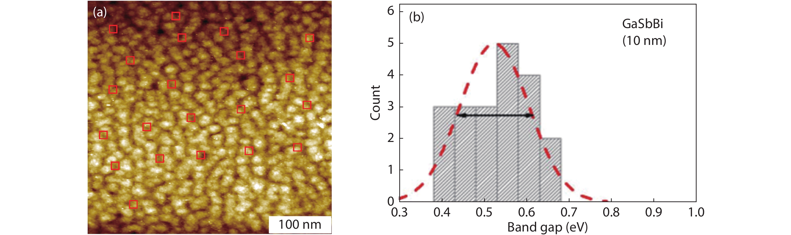
Abstract: The ultrahigh vacuum scanning tunneling microscope (STM) was used to characterize the GaSb1–xBix films of a few nanometers thickness grown by the molecular beam epitaxy (MBE) on the GaSb buffer layer of 100 nm with the GaSb (100) substrates. The thickness of the GaSb1–xBix layers of the samples are 5 and 10 nm, respectively. For comparison, the GaSb buffer was also characterized and its STM image displays terraces whose surfaces are basically atomically flat and their roughness is generally less than 1 monolayer (ML). The surface of 5 nm GaSb1–xBix film reserves the same terraced morphology as the buffer layer. In contrast, the morphology of the 10 nm GaSb1–xBix film changes to the mound-like island structures with a height of a few MLs. The result implies the growth mode transition from the two-dimensional mode as displayed by the 5 nm film to the Stranski–Krastinov mode as displayed by the 10 nm film. The statistical analysis with the scanning tunneling spectroscopy (STS) measurements indicates that both the incorporation and the inhomogeneity of Bi atoms increase with the thickness of the GaSb1–xBix layer.
Key words: scanning tunneling microscopy, molecular beam epitaxy, semiconductor surface
| [1] |
Li H D, Wang Z M. Bismuth-containing compounds. New York, NY: Springer New York, 2013
|
| [2] |
Luna E, Delorme O, Cerutti L, et al. Microstructure and interface analysis of emerging Ga(Sb, Bi) epilayers and Ga(Sb, Bi)/GaSb quantum wells for optoelectronic applications. Appl Phys Lett, 2018, 112, 151905 doi: 10.1063/1.5024199
|
| [3] |
Souto S, Hilska J, Galvão Gobato Y, et al. Raman spectroscopy of GaSb1−xBix alloys with high Bi content. Appl Phys Lett, 2020, 116, 202103 doi: 10.1063/5.0008100
|
| [4] |
Pan C B, Zha F X, Song Y X, et al. Spectral and spatial resolving of photoelectric property of femtosecond laser drilled holes of GaSb1−xBix. Opt Lett, 2015, 40, 3392 doi: 10.1364/OL.40.003392
|
| [5] |
Delorme O, Cerutti L, Luna E, et al. GaSbBi/GaSb quantum well laser diodes. Appl Phys Lett, 2017, 110, 222106 doi: 10.1063/1.4984799
|
| [6] |
Alberi K, Wu J, Walukiewicz W, et al. Valence-band anticrossing in mismatched III-V semiconductor alloys. Phys Rev B, 2007, 75, 045203 doi: 10.1103/PhysRevB.75.045203
|
| [7] |
Francoeur S, Seong M J, Mascarenhas A, et al. Band gap of GaAs1−xBix, 0 < x < 3.6%. Appl Phys Lett, 2003, 82, 3874 doi: 10.1063/1.1581983
|
| [8] |
Rajpalke M K, Linhart W M, Yu K M, et al. Bi-induced band gap reduction in epitaxial InSbBi alloys. Appl Phys Lett, 2014, 105, 212101 doi: 10.1063/1.4902442
|
| [9] |
Shalindar A J, Webster P T, Wilkens B J, et al. Measurement of InAsBi mole fraction and InBi lattice constant using Rutherford backscattering spectrometry and X-ray diffraction. J Appl Phys, 2016, 120, 145704 doi: 10.1063/1.4964799
|
| [10] |
Wang S M, Saha Roy I, Shi P X, et al. Growth of GaSb1–xBix by molecular beam epitaxy. J Vac Sci Technol B, 2012, 30, 02B114 doi: 10.1116/1.3672025
|
| [11] |
Delorme O, Cerutti L, Luna E, et al. Molecular-beam epitaxy of GaInSbBi alloys. J Appl Phys, 2019, 126, 155304 doi: 10.1063/1.5096226
|
| [12] |
Wang L J, Zhang L Y, Yue L, et al. Novel dilute bismide, epitaxy, physical properties and device application. Crystals, 2017, 7, 63 doi: 10.3390/cryst7030063
|
| [13] |
Rajpalke M K, Linhart W M, Birkett M, et al. High Bi content GaSbBi alloys. J Appl Phys, 2014, 116, 043511 doi: 10.1063/1.4891217
|
| [14] |
Yue L, Chen X, Zhang Y C, et al. Structural and optical properties of GaSbBi/GaSb quantum wells. Opt Mater Express, 2018, 8, 893 doi: 10.1364/OME.8.000893
|
| [15] |
Duzik A, Millunchick J M. Surface morphology and Bi incorporation in GaSbBi(As)/GaSb films. J Cryst Growth, 2014, 390, 5 doi: 10.1016/j.jcrysgro.2013.12.001
|
| [16] |
Yue L, Chen X, Zhang Y, et al. Molecular beam epitaxy growth and optical properties of high bismuth content GaSb1–xBix thin films. J Alloys Compnds, 2018, 742, 780 doi: 10.1016/j.jallcom.2018.01.329
|
| [17] |
Bauer E, van der Merwe J H. Structure and growth of crystalline superlattices: From monolayer to superlattice. Phys Rev B, 1986, 33, 3657 doi: 10.1103/PhysRevB.33.3657
|
| [18] |
Yamaguchi K, Yujobo K, Kaizu T. Stranski-Krastanov growth of InAs quantum dots with narrow size distribution. Jpn J Appl Phys, 2000, 39, L1245 doi: 10.1143/JJAP.39.L1245
|
| [19] |
Thibado P M, Bennett B R, Shanabrook B V, et al. A RHEED and STM study of Sb-rich AlSb and GaSb (001) surface reconstructions. J Cryst Growth, 1997, 175/176, 317 doi: 10.1016/S0022-0248(96)00982-7
|
| [20] |
Zha F X, Hong F, Pan B C, et al. Atomic resolution on the (111)B surface of mercury cadmium telluride by scanning tunneling microscopy. Phys Rev B, 2018, 97, 035401 doi: 10.1103/PhysRevB.97.035401
|
| [21] |
Feenstra R M. Tunneling spectroscopy of the (110) surface of direct-gap III–V semiconductors. Phys Rev B, 1994, 50, 4561 doi: 10.1103/PhysRevB.50.4561
|
| [22] |
Zha F X, Li M S, Shao J, et al. Implication of exotic topography depths of surface nanopits in scanning tunneling microscopy of HgCdTe. Appl Phys Lett, 2012, 101, 141604 doi: 10.1063/1.4756938
|
| [23] |
Polak M P, Scharoch P, Kudrawiec R. First-principles calculations of bismuth induced changes in the band structure of dilute Ga–V–Bi and In–V–Bi alloys: Chemical trends versus experimental data. Semicond Sci Technol, 2015, 30, 094001 doi: 10.1088/0268-1242/30/9/094001
|


Article views: 2466 Times PDF downloads: 44 Times Cited by: 0 Times
Received: 05 March 2021 Revised: 25 April 2021 Online: Accepted Manuscript: 28 May 2021Uncorrected proof: 08 June 2021Published: 01 September 2021
| Citation: |
Fangxing Zha, Qiuying Zhang, Haoguang Dai, Xiaolei Zhang, Li Yue, Shumin Wang, Jun Shao. The scanning tunneling microscopy and spectroscopy of GaSb1–xBix films of a few-nanometer thickness grown by molecular beam epitaxy[J]. Journal of Semiconductors, 2021, 42(9): 092101. doi: 10.1088/1674-4926/42/9/092101
F X Zha, Q Y Zhang, H G Dai, X L Zhang, L Yue, S M Wang, J Shao, The scanning tunneling microscopy and spectroscopy of GaSb1–xBix films of a few-nanometer thickness grown by molecular beam epitaxy[J]. J. Semicond., 2021, 42(9): 092101. doi: 10.1088/1674-4926/42/9/092101.
Export: BibTex EndNote

|
| [1] |
Li H D, Wang Z M. Bismuth-containing compounds. New York, NY: Springer New York, 2013
|
| [2] |
Luna E, Delorme O, Cerutti L, et al. Microstructure and interface analysis of emerging Ga(Sb, Bi) epilayers and Ga(Sb, Bi)/GaSb quantum wells for optoelectronic applications. Appl Phys Lett, 2018, 112, 151905 doi: 10.1063/1.5024199
|
| [3] |
Souto S, Hilska J, Galvão Gobato Y, et al. Raman spectroscopy of GaSb1−xBix alloys with high Bi content. Appl Phys Lett, 2020, 116, 202103 doi: 10.1063/5.0008100
|
| [4] |
Pan C B, Zha F X, Song Y X, et al. Spectral and spatial resolving of photoelectric property of femtosecond laser drilled holes of GaSb1−xBix. Opt Lett, 2015, 40, 3392 doi: 10.1364/OL.40.003392
|
| [5] |
Delorme O, Cerutti L, Luna E, et al. GaSbBi/GaSb quantum well laser diodes. Appl Phys Lett, 2017, 110, 222106 doi: 10.1063/1.4984799
|
| [6] |
Alberi K, Wu J, Walukiewicz W, et al. Valence-band anticrossing in mismatched III-V semiconductor alloys. Phys Rev B, 2007, 75, 045203 doi: 10.1103/PhysRevB.75.045203
|
| [7] |
Francoeur S, Seong M J, Mascarenhas A, et al. Band gap of GaAs1−xBix, 0 < x < 3.6%. Appl Phys Lett, 2003, 82, 3874 doi: 10.1063/1.1581983
|
| [8] |
Rajpalke M K, Linhart W M, Yu K M, et al. Bi-induced band gap reduction in epitaxial InSbBi alloys. Appl Phys Lett, 2014, 105, 212101 doi: 10.1063/1.4902442
|
| [9] |
Shalindar A J, Webster P T, Wilkens B J, et al. Measurement of InAsBi mole fraction and InBi lattice constant using Rutherford backscattering spectrometry and X-ray diffraction. J Appl Phys, 2016, 120, 145704 doi: 10.1063/1.4964799
|
| [10] |
Wang S M, Saha Roy I, Shi P X, et al. Growth of GaSb1–xBix by molecular beam epitaxy. J Vac Sci Technol B, 2012, 30, 02B114 doi: 10.1116/1.3672025
|
| [11] |
Delorme O, Cerutti L, Luna E, et al. Molecular-beam epitaxy of GaInSbBi alloys. J Appl Phys, 2019, 126, 155304 doi: 10.1063/1.5096226
|
| [12] |
Wang L J, Zhang L Y, Yue L, et al. Novel dilute bismide, epitaxy, physical properties and device application. Crystals, 2017, 7, 63 doi: 10.3390/cryst7030063
|
| [13] |
Rajpalke M K, Linhart W M, Birkett M, et al. High Bi content GaSbBi alloys. J Appl Phys, 2014, 116, 043511 doi: 10.1063/1.4891217
|
| [14] |
Yue L, Chen X, Zhang Y C, et al. Structural and optical properties of GaSbBi/GaSb quantum wells. Opt Mater Express, 2018, 8, 893 doi: 10.1364/OME.8.000893
|
| [15] |
Duzik A, Millunchick J M. Surface morphology and Bi incorporation in GaSbBi(As)/GaSb films. J Cryst Growth, 2014, 390, 5 doi: 10.1016/j.jcrysgro.2013.12.001
|
| [16] |
Yue L, Chen X, Zhang Y, et al. Molecular beam epitaxy growth and optical properties of high bismuth content GaSb1–xBix thin films. J Alloys Compnds, 2018, 742, 780 doi: 10.1016/j.jallcom.2018.01.329
|
| [17] |
Bauer E, van der Merwe J H. Structure and growth of crystalline superlattices: From monolayer to superlattice. Phys Rev B, 1986, 33, 3657 doi: 10.1103/PhysRevB.33.3657
|
| [18] |
Yamaguchi K, Yujobo K, Kaizu T. Stranski-Krastanov growth of InAs quantum dots with narrow size distribution. Jpn J Appl Phys, 2000, 39, L1245 doi: 10.1143/JJAP.39.L1245
|
| [19] |
Thibado P M, Bennett B R, Shanabrook B V, et al. A RHEED and STM study of Sb-rich AlSb and GaSb (001) surface reconstructions. J Cryst Growth, 1997, 175/176, 317 doi: 10.1016/S0022-0248(96)00982-7
|
| [20] |
Zha F X, Hong F, Pan B C, et al. Atomic resolution on the (111)B surface of mercury cadmium telluride by scanning tunneling microscopy. Phys Rev B, 2018, 97, 035401 doi: 10.1103/PhysRevB.97.035401
|
| [21] |
Feenstra R M. Tunneling spectroscopy of the (110) surface of direct-gap III–V semiconductors. Phys Rev B, 1994, 50, 4561 doi: 10.1103/PhysRevB.50.4561
|
| [22] |
Zha F X, Li M S, Shao J, et al. Implication of exotic topography depths of surface nanopits in scanning tunneling microscopy of HgCdTe. Appl Phys Lett, 2012, 101, 141604 doi: 10.1063/1.4756938
|
| [23] |
Polak M P, Scharoch P, Kudrawiec R. First-principles calculations of bismuth induced changes in the band structure of dilute Ga–V–Bi and In–V–Bi alloys: Chemical trends versus experimental data. Semicond Sci Technol, 2015, 30, 094001 doi: 10.1088/0268-1242/30/9/094001
|

 WeChat ID
Journal of Semiconductors © 2017 All Rights Reserved 京ICP备05085259号-2

 DownLoad:

