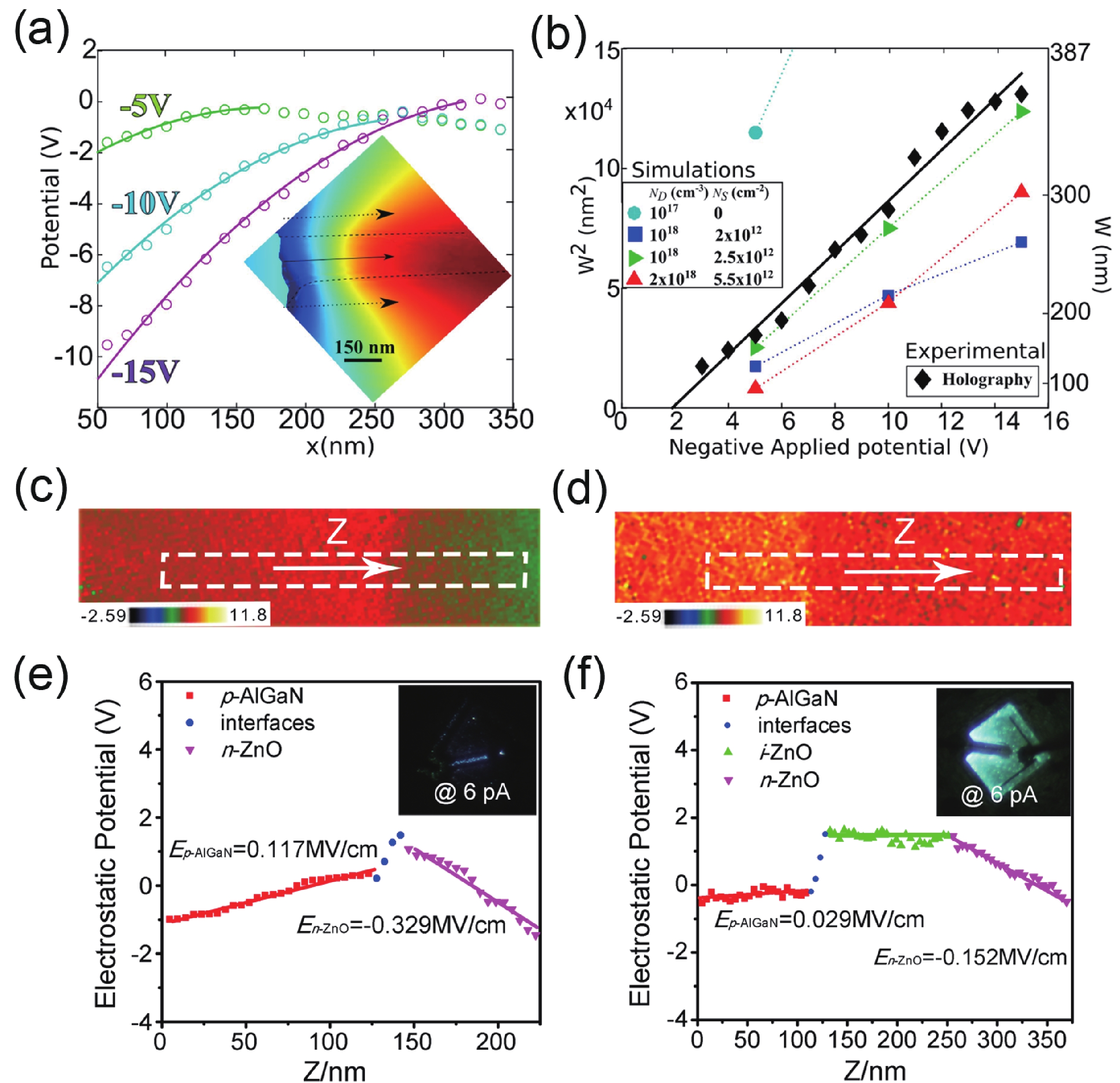
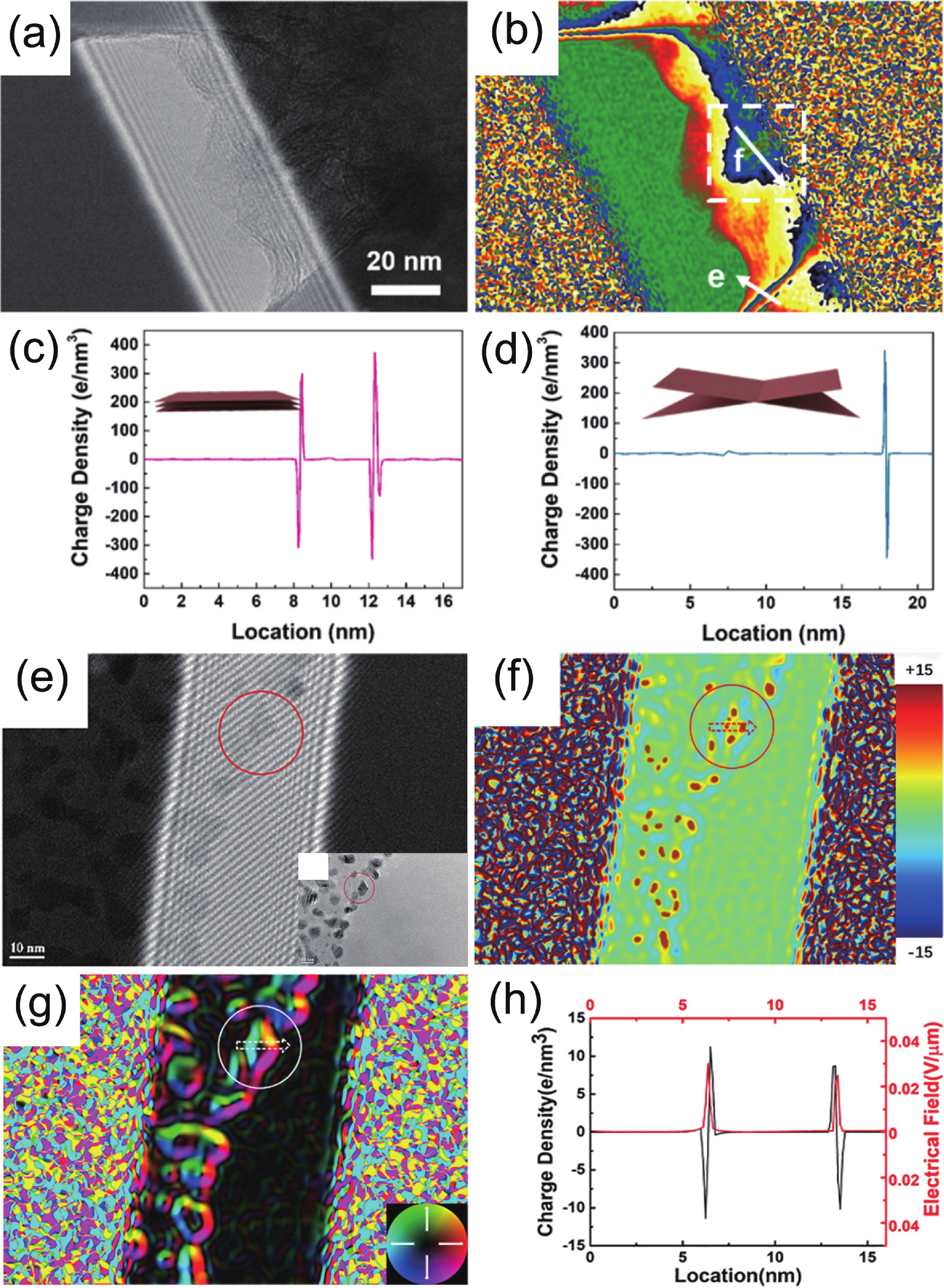
| [1] |
Waldrop M M. The chips are down for Moore's law. Nature, 2016, 530, 144 doi: 10.1038/530144a |
| [2] |
Li L, Gan Z, McCartney M R, et al. Atomic configurations at InAs partial dislocation cores associated with Z-shape faulted dipoles. Sci Rep, 2013, 3, 3229 doi: 10.1038/srep03229 |
| [3] |
Li L, Tu F, Jin L, et al. Polarity continuation and frustration in ZnSe nanospirals. Sci Rep, 2014, 4, 7447 doi: 10.1038/srep07447 |
| [4] |
Smith D J. Atomic-resolution structure imaging of defects and interfaces in compound semiconductors. Prog Cryst Growth Charact Mater, 2020, 66, 100498 doi: 10.1016/j.pcrysgrow.2020.100498 |
| [5] |
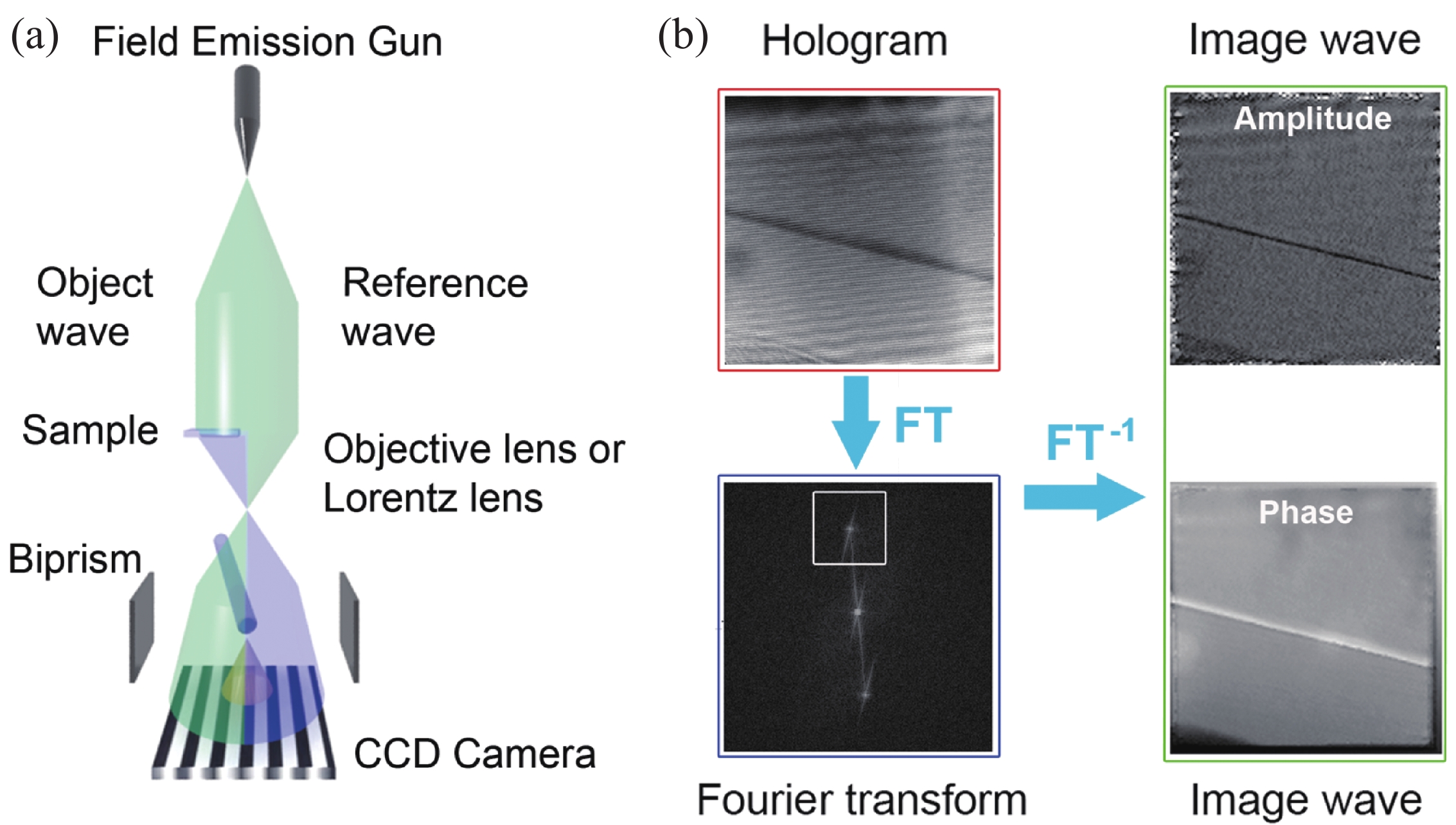
Bragg W L. Microscopy by reconstructed wave-fronts. Nature, 1950, 166, 399 doi: 10.1038/166399b0 |
| [6] |
Crewe A V, Isaacson M, Johnson D. A simple scanning electron microscope. Rev Sci Instrum, 1969, 40, 241 doi: 10.1063/1.1683910 |
| [7] |
|
| [8] |
Li L Y, Hu X K, Gao Y H. Electron holographic study of semiconductor light-emitting diodes. Small, 2018, 14, 1701996 doi: 10.1002/smll.201701996 |
| [9] |
|
| [10] |
McCartney M R, Gajdardziska-Josifovska M. Absolute measurement of normalized thickness, t/ λ i, from off-axis electron holography. Ultramicroscopy, 1994, 53, 283 doi: 10.1016/0304-3991(94)90040-X |
| [11] |
Gribelyuk M A, McCartney M R, Li J, et al. Mapping of electrostatic potential in deep submicron CMOS devices by electron holography. Phys Rev Lett, 2002, 89, 025502 doi: 10.1103/PhysRevLett.89.025502 |
| [12] |
den Hertog M I, Schmid H, Cooper D, et al. Mapping active dopants in single silicon nanowires using off-axis electron holography. Nano Lett, 2009, 9, 3837 doi: 10.1021/nl902024h |
| [13] |
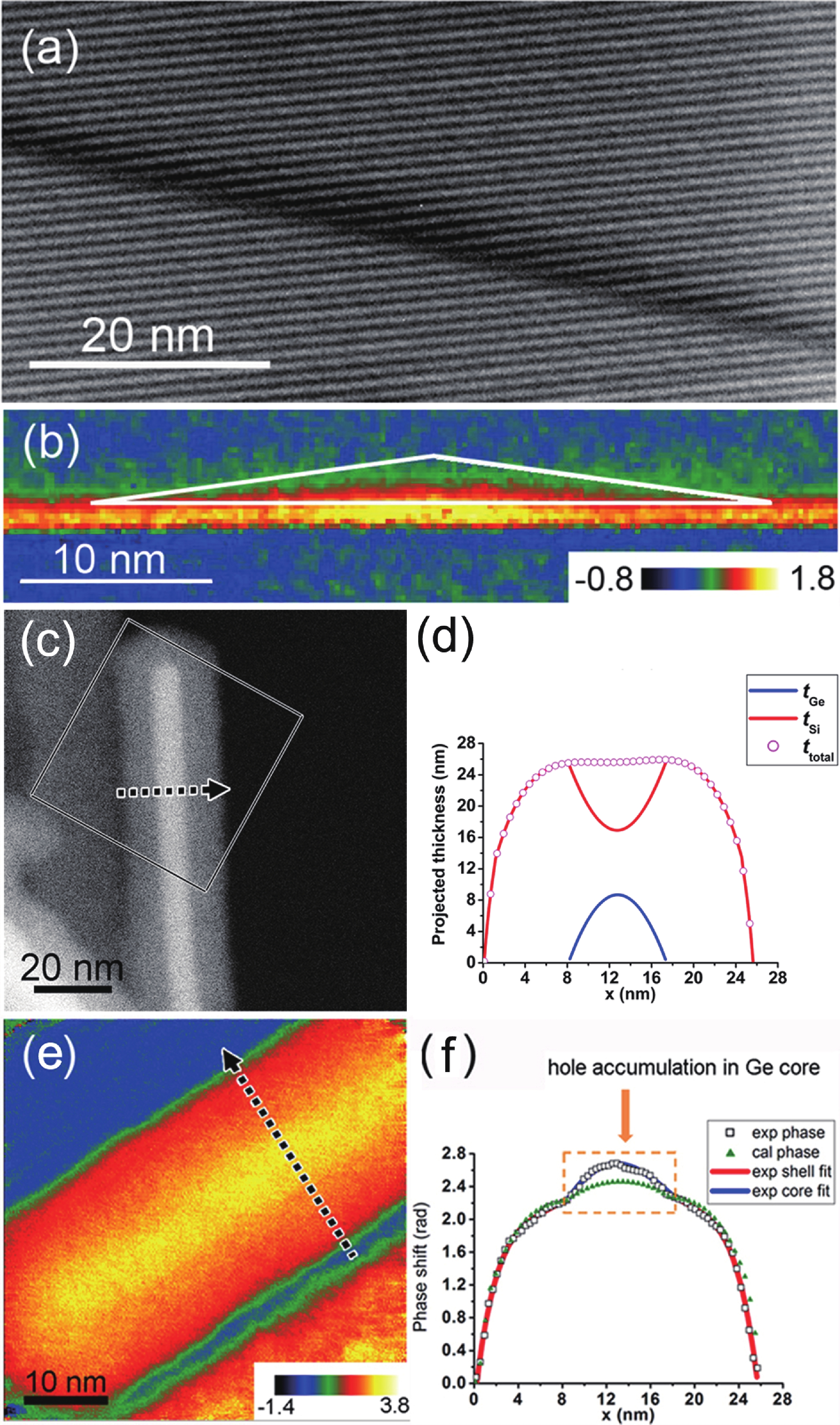
Li L Y, Smith D J, Dailey E, et al. Observation of hole accumulation in Ge/Si core/shell nanowires using off-axis electron holography. Nano Lett, 2011, 11, 493 doi: 10.1021/nl1033107 |
| [14] |
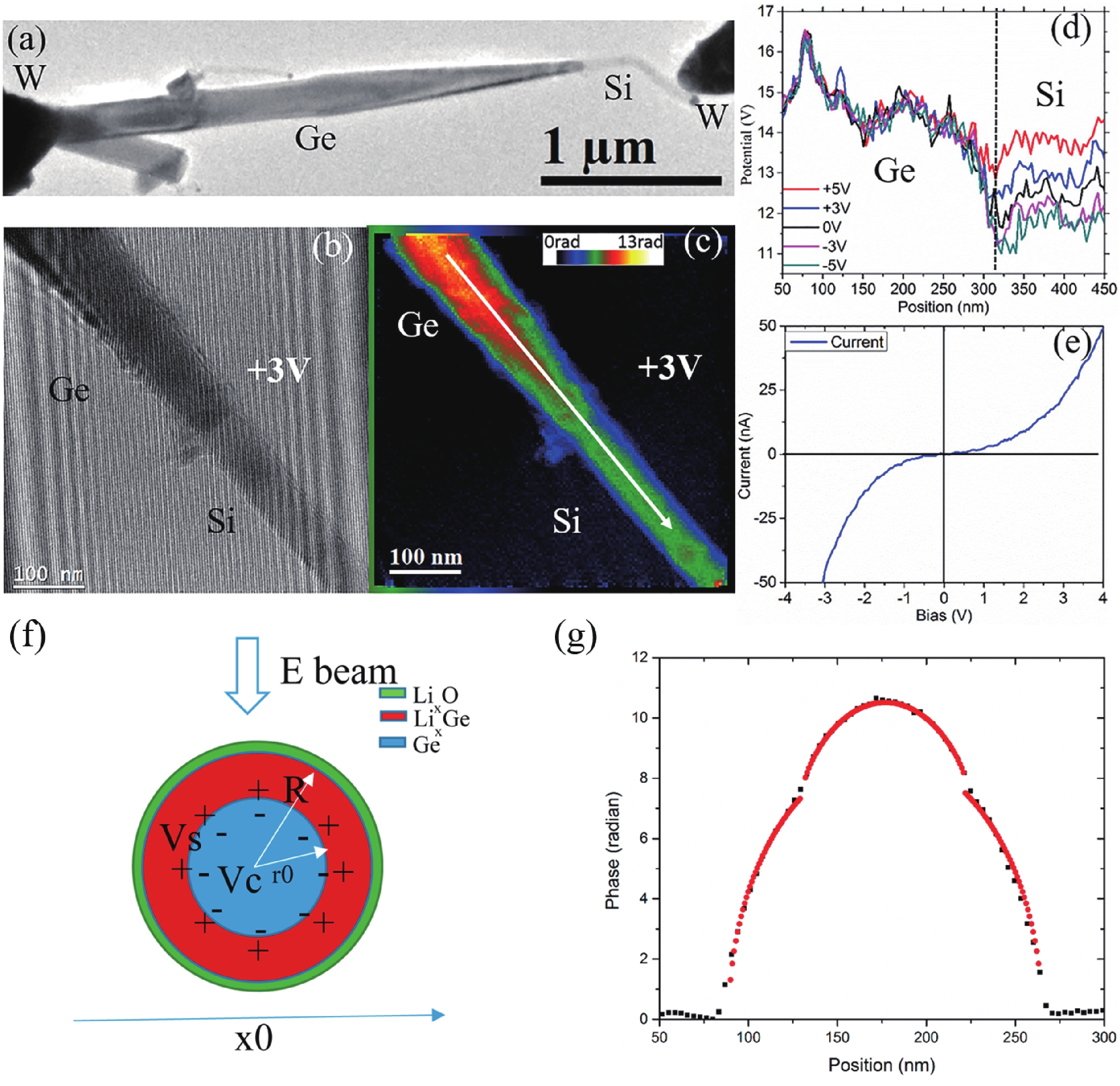
Gan Z F, Gu M, Tang J S, et al. Direct mapping of charge distribution during lithiation of Ge nanowires using off-axis electron holography. Nano Lett, 2016, 16, 3748 doi: 10.1021/acs.nanolett.6b01099 |
| [15] |
Zhou L, Smith D J, McCartney M R, et al. Measurement of electric field across individual wurtzite GaN quantum dots using electron holography. Appl Phys Lett, 2011, 99, 101905 doi: 10.1063/1.3636109 |
| [16] |
McCartney M R, Dunin-Borkowski R E, Smith D J. Quantitative measurement of nanoscale electrostatic potentials and charges using off-axis electron holography: Developments and opportunities. Ultramicroscopy, 2019, 203, 105 doi: 10.1016/j.ultramic.2019.01.008 |
| [17] |
Kern F, Linck M, Wolf D, et al. Autocorrected off-axis holography of two-dimensional materials. Phys Rev Res, 2020, 2, 043360 doi: 10.1103/PhysRevResearch.2.043360 |
| [18] |
Li L Y, Ketharanathan S, Drucker J, et al. Study of hole accumulation in individual germanium quantum dots in p-type silicon by off-axis electron holography. Appl Phys Lett, 2009, 94, 232108 doi: 10.1063/1.3154524 |
| [19] |
Gan Z F, Perea D E, Yoo J, et al. Characterization of electrical properties in axial Si-Ge nanowire heterojunctions using off-axis electron holography and atom-probe tomography. J Appl Phys, 2016, 120, 104301 doi: 10.1063/1.4962380 |
| [20] |
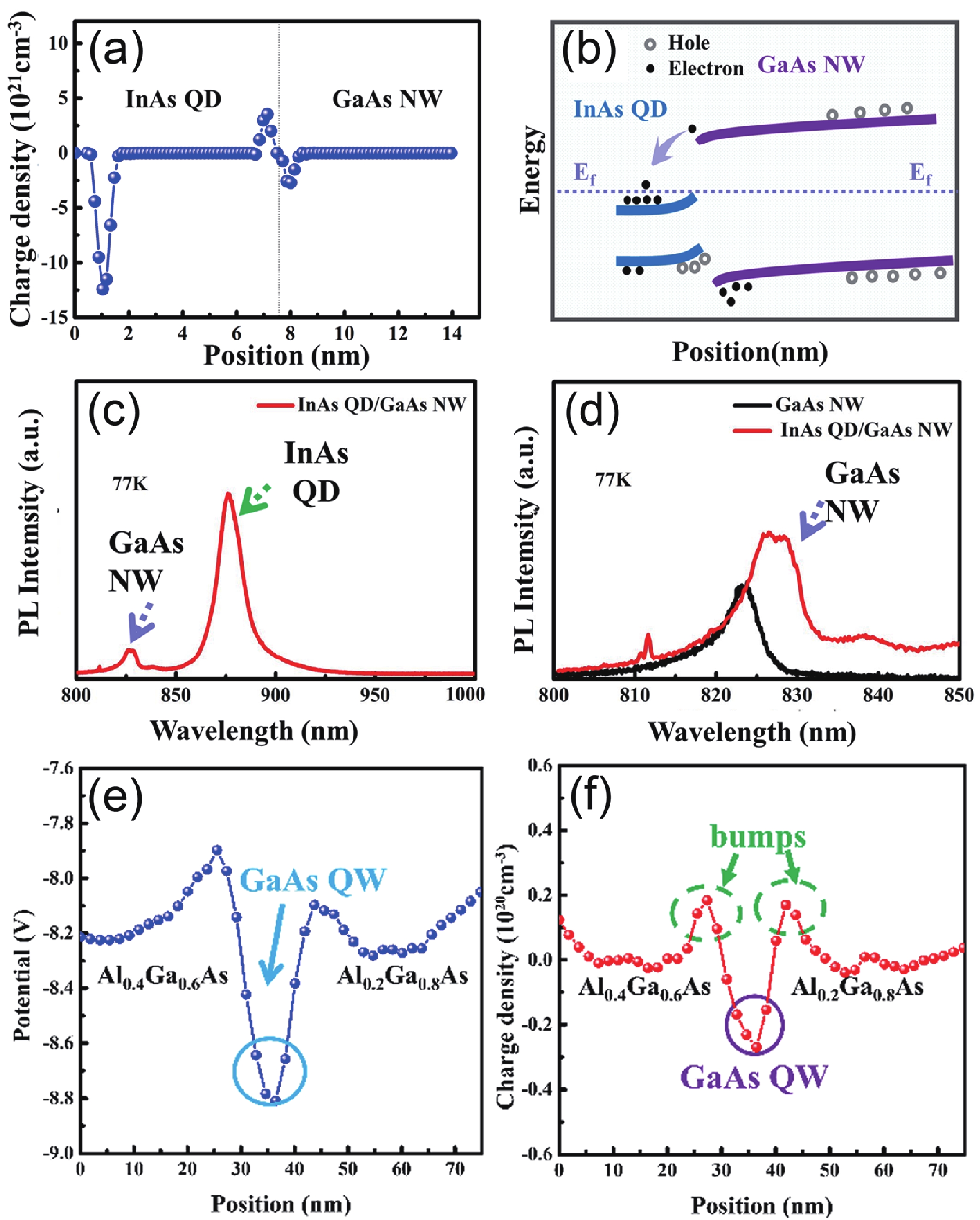
Cheng F, Li B, Li L Y, et al. Study of the polarization effect in InAs quantum dots/GaAs nanowires. J Phys Chem C, 2019, 123, 4228 doi: 10.1021/acs.jpcc.8b11425 |
| [21] |
Li C, Cheng Y F, Li B, et al. Study of charge distributions and electrical properties in GaAs/AlGaAs single quantum well/nanowire heterostructures. J Phys Chem C, 2019, 123, 26888 doi: 10.1021/acs.jpcc.9b06371 |
| [22] |
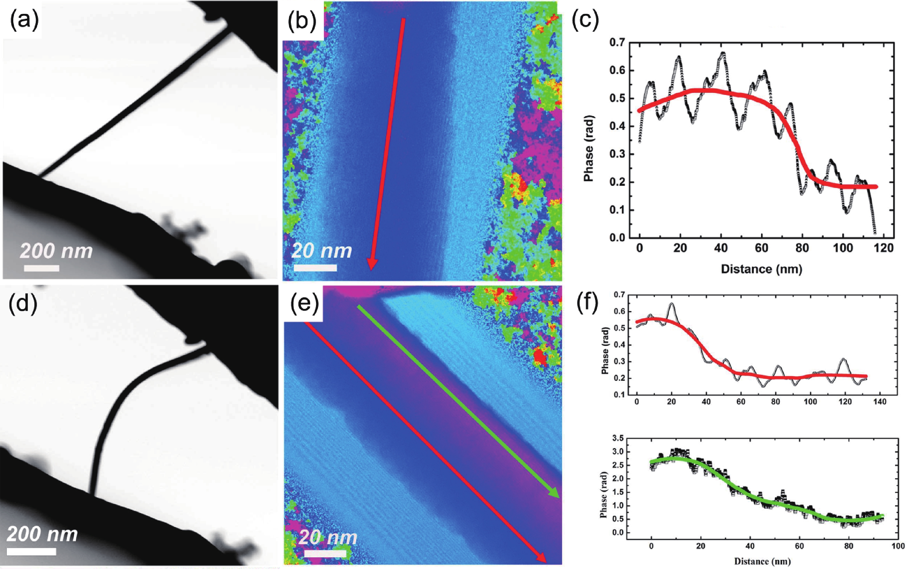
Qi T Y, Cheng Y F, Cheng F, et al. Study of nanometer-scale structures and electrostatic properties of InAs quantum dots decorating GaAs/AlAs core/shell nanowires. Nanotechnology, 2020, 31, 245701 doi: 10.1088/1361-6528/ab767e |
| [23] |
den Hertog M, Songmuang R, Monroy E. Polarization fields in GaN/AlN nanowire heterostructures studied by off-axis holography. J Phys: Conf Ser, 2013, 471, 012019 doi: 10.1088/1742-6596/471/1/012019 |
| [24] |
Chen X, Wang Y G, Guo J, et al. In-situ potential mapping of space charge layer in GaN nanowires under electrical field by off-axis electron holography. Prog Nat Sci Mater Int, 2016, 26, 163 doi: 10.1016/j.pnsc.2016.03.009 |
| [25] |
Chen X, Wang Y G, Jian J K, et al. Effect of strain on space charge layer in GaN nanowires investigated by in situ off-axis electron holography. Prog Nat Sci Mater Int, 2017, 27, 186 doi: 10.1016/j.pnsc.2017.02.003 |
| [26] |
Chen X, Wang Y G, Jian J K, et al. Controlling charges distribution at the surface of a single GaN nanowire by in situ strain. Prog Nat Sci Mater Int, 2017, 27, 430 doi: 10.1016/j.pnsc.2017.06.007 |
| [27] |
den Hertog M, Donatini F, McLeod R, et al. In situ biasing and off-axis electron holography of a ZnO nanowire. Nanotechnology, 2018, 29, 025710 doi: 10.1088/1361-6528/aa923c |
| [28] |
Jiang F, Chen J W, Bi H, et al. The underlying micro-mechanism of performance enhancement of non-polar n-ZnO/p-AlGaN ultraviolet light emitting diode with i-ZnO inserted layer. Appl Phys Lett, 2018, 112, 033505 doi: 10.1063/1.5010594 |
| [29] |
Li X, Wen C Y, Yang L T, et al. Enhanced visualizing charge distribution of 2D/2D MXene/MoS 2 heterostructure for excellent microwave absorption performance. J Alloys Compd, 2021, 869, 159365 doi: 10.1016/j.jallcom.2021.159365 |
| [30] |
Xing L S, Li X, Wu Z C, et al. 3D hierarchical local heterojunction of MoS 2/FeS 2 for enhanced microwave absorption. Chem Eng J, 2020, 379, 122241 doi: 10.1016/j.cej.2019.122241 |
| [31] |
Kawasaki T, Takahashi Y, Tanigaki T. Holography: application to high-resolution imaging. Microscopy, 2020, 70, 39 doi: 10.1093/jmicro/dfaa050 |
| [32] |
Wolf D, Lubk A, Prete P, et al. 3D mapping of nanoscale electric potentials in semiconductor structures using electron-holographic tomography. J Phys D, 2016, 49, 364004 doi: 10.1088/0022-3727/49/36/364004 |
| [33] |
Liu L Z Y, McAleese C, Sridhara Rao D V, et al. Electron holography of an in situ biased GaN-based LED. Phys Status Solidi C, 2012, 9, 704 doi: 10.1002/pssc.201100486 |
| [34] |
Yazdi S, Kasama T, Beleggia M, et al. Towards quantitative electrostatic potential mapping of working semiconductor devices using off-axis electron holography. Ultramicroscopy, 2015, 152, 10 doi: 10.1016/j.ultramic.2014.12.012 |


 DownLoad: