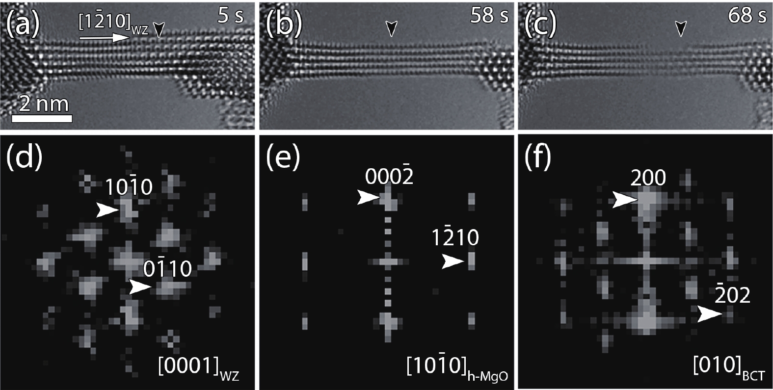
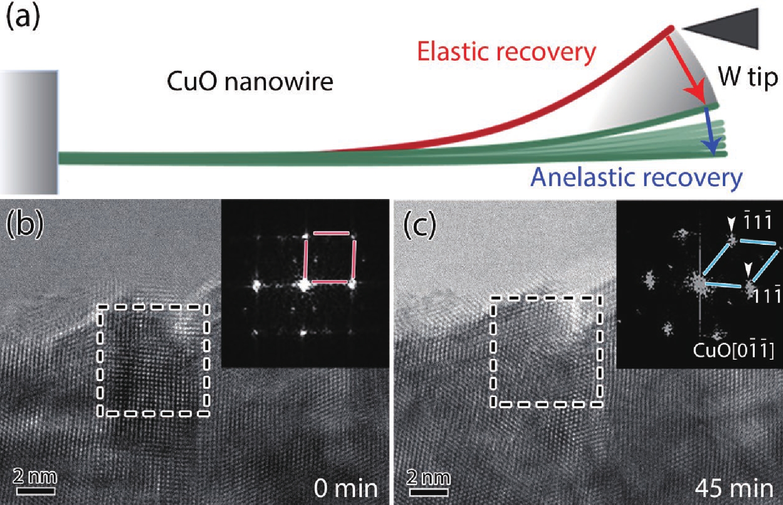
| [1] |
Sheng J Z, Han K L, Hong T H, et al. Review of recent progresses on flexible oxide semiconductor thin film transistors based on atomic layer deposition processes. J Semicond, 2018, 39, 011008 doi: 10.1088/1674-4926/39/1/011008 |
| [2] |
Park J S, Kim H, Kim I D. Overview of electroceramic materials for oxide semiconductor thin film transistors. J Electroceram, 2014, 32, 117 doi: 10.1007/s10832-013-9858-0 |
| [3] |
Dos Santos C L, Piquini P. Diameter dependence of mechanical, electronic, and structural properties of InAs and InP nanowires: a first-principles study. Phys Rev B, 2010, 81, 075408 doi: 10.1103/PhysRevB.81.075408 |
| [4] |
Rim Y S, Chen H J, Zhu B W, et al. Interface engineering of metal oxide semiconductors for biosensing applications. Adv Mater Interfaces, 2017, 4, 1700020 doi: 10.1002/admi.201700020 |
| [5] |
Csiszar G, Lawitzki R, Everett C, et al. Elastic behavior of Nb 2O 5/Al 2O 3 core-shell nanowires in terms of short-range-order structures. ACS Appl Mater Interfaces, 2021, 13, 24238 doi: 10.1021/acsami.1c02936 |
| [6] |
|
| [7] |
Li S, Zhang M, Wang H. Simulation of gas sensing mechanism of porous metal oxide semiconductor sensor based on finite element analysis. Sci Rep, 2021, 11, 17158 doi: 10.1038/s41598-021-96591-2 |
| [8] |
Ke Y J, Chen J W, Lin G J, et al. Smart windows: electro-, thermo-, mechano-, photochromics, and beyond. Adv Energy Mater, 2019, 9, 1902066 doi: 10.1002/aenm.201902066 |
| [9] |
Alus L, Brontvein O, Kossoy A, et al. Aligned growth of semiconductor nanowires on scratched amorphous substrates. Adv Funct Mater, 2021, 31, 2103950 doi: 10.1002/adfm.202103950 |
| [10] |
Chen H D, Zhang Z, Huang B J, et al. Progress in complementary metal-oxide-semiconductor silicon photonics and optoelectronic integrated circuits. J Semicond, 2015, 36, 121001 doi: 10.1088/1674-4926/36/12/121001 |
| [11] |
Troughton J, Atkinson D. Amorphous InGaZnO and metal oxide semiconductor devices: an overview and current status. J Mater Chem C, 2019, 7, 12388 doi: 10.1039/C9TC03933C |
| [12] |
Perrotta A, Pilz J, Milella A, et al. Opto-chemical control through thermal treatment of plasma enhanced atomic layer deposited ZnO: an in situ study. Appl Surf Sci, 2019, 483, 10 doi: 10.1016/j.apsusc.2019.03.122 |
| [13] |
Hofmann A I, Cloutet E, Hadziioannou G. Materials for transparent electrodes: from metal oxides to organic alternatives. Adv Electron Mater, 2018, 4, 1700412 doi: 10.1002/aelm.201700412 |
| [14] |
Yu X, Marks T J, Facchetti A. Metal oxides for optoelectronic applications. Nat Mater, 2016, 15, 383 doi: 10.1038/nmat4599 |
| [15] |
Wang L H, Kong D L, Xin T J, et al. Deformation mechanisms of bent Si nanowires governed by the sign and magnitude of strain. Appl Phys Lett, 2016, 108, 151903 doi: 10.1063/1.4946855 |
| [16] |
Minamisawa R A, Suess M J, Spolenak R, et al. Top-down fabricated silicon nanowires under tensile elastic strain up to 4.5%. Nat Commun, 2012, 3, 1096 doi: 10.1038/ncomms2102 |
| [17] |
Zhang C, Kvashnin D G, Bourgeois L, et al. Mechanical, electrical, and crystallographic property dynamics of bent and strained Ge/Si core-shell nanowires as revealed by in situ transmission electron microscopy. Nano Lett, 2018, 18, 7238 doi: 10.1021/acs.nanolett.8b03398 |
| [18] |
Han X, Kou L, Lang X, et al. Electronic and mechanical coupling in bent ZnO nanowires. Adv Mater, 2009, 21, 4937 doi: 10.1002/adma.200900956 |
| [19] |
Li J, Shan Z W, Ma E. Elastic strain engineering for unprecedented materials properties. MRS Bull, 2014, 39, 108 doi: 10.1557/mrs.2014.3 |
| [20] |
Jia L, Shu D J, Wang M. Tuning the area percentage of reactive surface of TiO 2 by strain engineering. Phys Rev Lett, 2012, 109, 156104 doi: 10.1103/PhysRevLett.109.156104 |
| [21] |
Thulin L, Guerra J. Calculations of strain-modified anatase TiO 2 band structures. Phys Rev B, 2008, 77, 195112 doi: 10.1103/PhysRevB.77.195112 |
| [22] |
Lim B, Cui X Y, Ringer S P. Strain-mediated bandgap engineering of straight and bent semiconductor nanowires. Phys Chem Chem Phys, 2021, 23, 5407 doi: 10.1039/D1CP00457C |
| [23] |
Bao P T, Wang Y B, Cui X Y, et al. Atomic-scale observation of parallel development of super elasticity and reversible plasticity in GaAs nanowires. Appl Phys Lett, 2014, 104, 021904 doi: 10.1063/1.4861846 |
| [24] |
Chen B, Gao Q, Wang Y B, et al. Anelastic behavior in GaAs semiconductor nanowires. Nano Lett, 2013, 13, 3169 doi: 10.1021/nl401175t |
| [25] |
Han X D, Zhang Y F, Zheng K, et al. Low-temperature in situ large strain plasticity of ceramic SiC nanowires and its atomic-scale mechanism. Nano Lett, 2007, 7, 452 doi: 10.1021/nl0627689 |
| [26] |
Wei B, Zheng K, Ji Y, et al. Size-dependent bandgap modulation of ZnO nanowires by tensile strain. Nano Lett, 2012, 12, 4595 doi: 10.1021/nl301897q |
| [27] |
Sheng H P, Zheng H, Cao F, et al. Anelasticity of twinned CuO nanowires. Nano Res, 2015, 8, 3687 doi: 10.1007/s12274-015-0868-x |
| [28] |
Varghese B, Zhang Y, Feng Y P, et al. Probing the size-structure-property correlation of individual nanowires. Phys Rev B, 2009, 79, 115419 doi: 10.1103/PhysRevB.79.115419 |
| [29] |
Liu K H, Wang W L, Xu Z, et al. In situ probing mechanical properties of individual tungsten oxide nanowires directly grown on tungsten tips inside transmission electron microscope. Appl Phys Lett, 2006, 89, 221908 doi: 10.1063/1.2397547 |
| [30] |
Agrawal R, Paci J T, Espinosa H D. Large-scale density functional theory investigation of failure modes in ZnO nanowires. Nano Lett, 2010, 10, 3432 doi: 10.1021/nl1014926 |
| [31] |
Wang L H, Zhang Z, Han X D. In situ experimental mechanics of nanomaterials at the atomic scale. npg Asia Mater, 2013, 5, e40 doi: 10.1038/am.2012.70 |
| [32] |
Zheng H, Cao F, Zhao L, et al. Atomistic and dynamic structural characterizations in low-dimensional materials: recent applications of in situ transmission electron microscopy. Microscopy, 2019, 68, 423 doi: 10.1093/jmicro/dfz038 |
| [33] |
Sheng H, Zheng H, Jia S, et al. Atomistic manipulation of reversible oxidation and reduction in Ag with an electron beam. Nanoscale, 2019, 11, 10756 doi: 10.1039/C8NR09525F |
| [34] |
Liu H H, Zheng H, Li L, et al. Surface-coating-mediated electrochemical performance in CuO nanowires during the sodiation-desodiation cycling. Adv Mater Interfaces, 2018, 5, 1701255 doi: 10.1002/admi.201701255 |
| [35] |
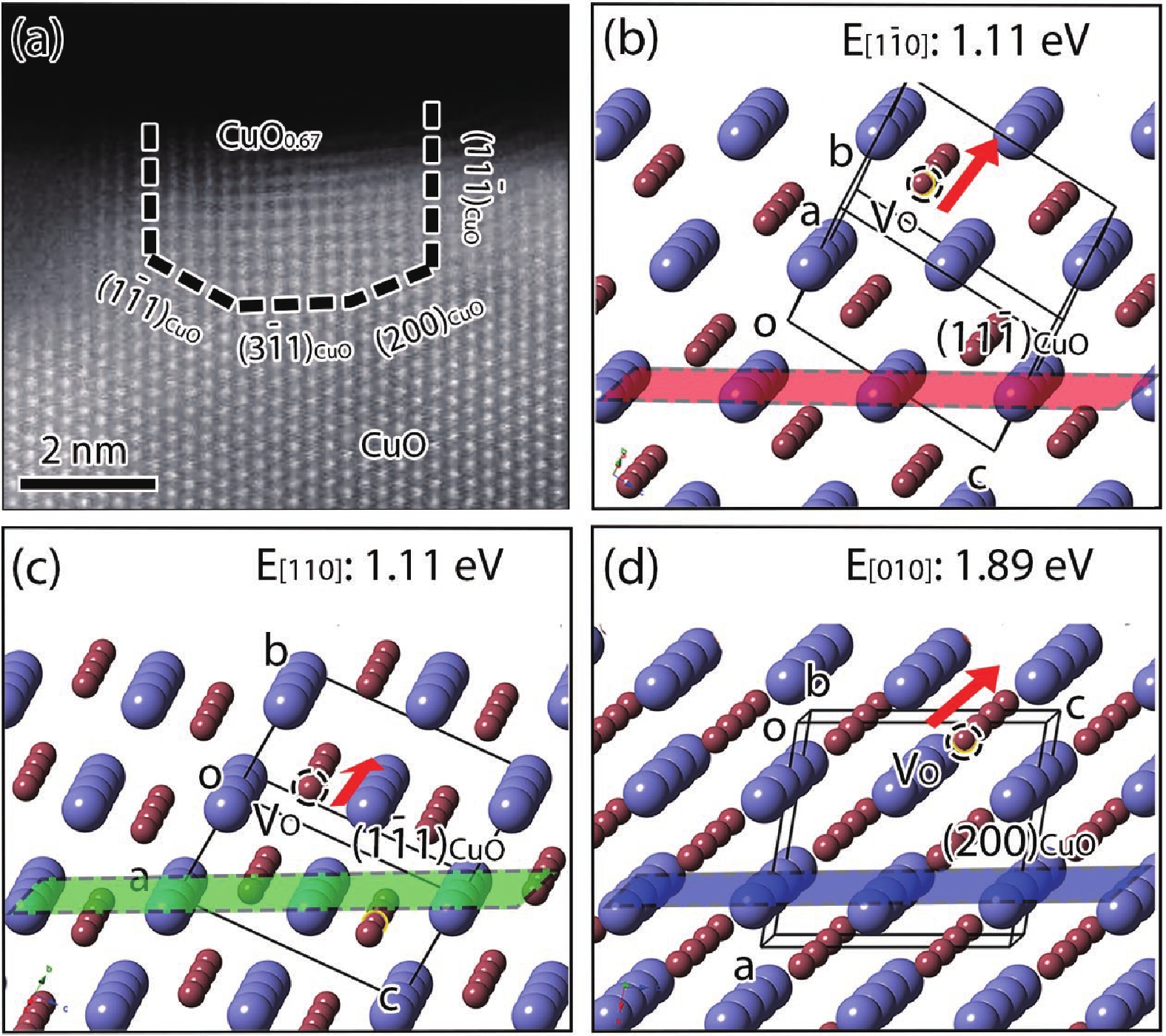
Jia S, Hu S, Zheng H, et al. Atomistic interface dynamics in Sn-catalyzed growth of wurtzite and zinc-blende ZnO nanowires. Nano Lett, 2018, 18, 4095 doi: 10.1021/acs.nanolett.8b00420 |
| [36] |
Zheng H, Wang J, Huang J Y, et al. Void-assisted plasticity in Ag nanowires with a single twin structure. Nanoscale, 2014, 6, 9574 doi: 10.1039/C3NR04731H |
| [37] |
Zheng H, Wang J, Huang J Y, et al. In situ visualization of birth and annihilation of grain boundaries in an Au nanocrystal. Phys Rev Lett, 2012, 109, 225501 doi: 10.1103/PhysRevLett.109.225501 |
| [38] |
Zhang J, Li Y, Li X, et al. Timely and atomic-resolved high-temperature mechanical investigation of ductile fracture and atomistic mechanisms of tungsten. Nat Commun, 2021, 12, 2218 doi: 10.1038/s41467-021-22447-y |
| [39] |
Chen S, Oh H S, Gludovatz B, et al. Real-time observations of TRIP-induced ultrahigh strain hardening in a dual-phase CrMnFeCoNi high-entropy alloy. Nat Commun, 2020, 11, 826 doi: 10.1038/s41467-020-14641-1 |
| [40] |
Liu B Y, Liu F, Yang N, et al. Large plasticity in magnesium mediated by pyramidal dislocations. Science, 2019, 365, 73 doi: 10.1126/science.aaw2843 |
| [41] |
Wang S, Shan Z, Huang H. The mechanical properties of nanowires. Adv Sci, 2017, 4, 1600332 doi: 10.1002/advs.201600332 |
| [42] |
Huang J Y, Zheng H, Mao S X, et al. In situ nanomechanics of GaN nanowires. Nano Lett, 2011, 11, 1618 doi: 10.1021/nl200002x |
| [43] |
Huang L L, Zheng F Y, Deng Q M, et al. In situ scanning transmission electron microscopy observations of fracture at the atomic scale. Phys Rev Lett, 2020, 125, 246102 doi: 10.1103/PhysRevLett.125.246102 |
| [44] |
Agrawal R, Peng B, Espinosa H D. Experimental-computational investigation of ZnO nanowires strength and fracture. Nano Lett, 2009, 9, 4177 doi: 10.1021/nl9023885 |
| [45] |
Wang Q, Wang J, Li J, et al. Consecutive crystallographic reorientations and superplasticity in body-centered cubic niobium nanowires. Sci Adv, 2018, 4, eaas8850 doi: 10.1126/sciadv.aas8850 |
| [46] |
Wang L H, Liu P, Guan P, et al. In situ atomic-scale observation of continuous and reversible lattice deformation beyond the elastic limit. Nat Commun, 2013, 4, 2413 doi: 10.1038/ncomms3413 |
| [47] |
Stinville J C, Charpagne M A, Bourdin F, et al. Measurement of elastic and rotation fields during irreversible deformation using Heaviside-digital image correlation. Mater Charact, 2020, 169, 110600 doi: 10.1016/j.matchar.2020.110600 |
| [48] |
Agrawal R, Peng B, Gdoutos E E, et al. Elasticity size effects in ZnO nanowires – a combined experimental-computational approach. Nano Lett, 2008, 8, 3668 doi: 10.1021/nl801724b |
| [49] |
Wang G, and Li X. Size dependency of the elastic modulus of ZnO nanowires: Surface stress effect. Appl Phys Lett, 2007, 91, 242 doi: 10.1063/1.2821118 |
| [50] |
Wang J, Kulkarni A J, Ke F J, et al. Novel mechanical behavior of ZnO nanorods. Comput Methods Appl Mech Eng, 2008, 197, 3182 doi: 10.1016/j.cma.2007.10.011 |
| [51] |
Cao F, Li L, Zheng H, et al. Controllable elasticity storage and release in CuO-Pt core-shell nanowires. ChemNanoMat, 2018, 4, 1140 doi: 10.1002/cnma.201800368 |
| [52] |
Egbo K O, Liu C P, Ekuma C E, et al. Vacancy defects induced changes in the electronic and optical properties of NiO studied by spectroscopic ellipsometry and first-principles calculations. J Appl Phys, 2020, 128, 135705 doi: 10.1063/5.0021650 |
| [53] |
Zhang J, Shi J, Qi D C, et al. Recent progress on the electronic structure, defect, and doping properties of Ga 2O 3. APL Mater, 2020, 8, 020906 doi: 10.1063/1.5142999 |
| [54] |
Lu Z, Huang B, Li G, et al. Shear induced deformation twinning evolution in thermoelectric InSb. npj Comput Mater, 2021, 7, 111 doi: 10.1038/s41524-021-00581-x |
| [55] |
Wei S, Wang Q, Wei H, et al. Bending-induced deformation twinning in body-centered cubic tungsten nanowires. Mater Res Lett, 2019, 7, 210 doi: 10.1080/21663831.2019.1578833 |
| [56] |
Wang J, Zeng Z, Wen M, et al. Anti-twinning in nanoscale tungsten. Sci Adv, 2020, 6, eaay2792 doi: 10.1126/sciadv.aay2792 |
| [57] |
Chen Y, Burgess T, An X, et al. Effect of a high density of stacking faults on the Young's modulus of GaAs nanowires. Nano Lett, 2016, 16, 1911 doi: 10.1021/acs.nanolett.5b05095 |
| [58] |
Mignerot F, Kedjar B, Bahsoun H, et al. Size-induced twinning in InSb semiconductor during room temperature deformation. Sci Rep, 2021, 11, 19441 doi: 10.1038/s41598-021-98492-w |
| [59] |
Dai S, Zhao J, He M R, et al. Elastic properties of GaN nanowires: revealing the influence of planar defects on Young's modulus at nanoscale. Nano Lett, 2015, 15, 8 doi: 10.1021/nl501986d |
| [60] |
Cao F, Jia S F, Zheng H, et al. Thermal-induced formation of domain structures in CuO nanomaterials. Phys Rev Mater, 2017, 1, 053401 doi: 10.1103/PhysRevMaterials.1.053401 |
| [61] |
Wang L, Zheng K, Zhang Z, et al. Direct atomic-scale imaging about the mechanisms of ultralarge bent straining in Si nanowires. Nano Lett, 2011, 11, 2382 doi: 10.1021/nl200735p |
| [62] |
Dhanaraj G, Dudley M, Bliss D, et al. Growth and process induced dislocations in zinc oxide crystals. J Cryst Growth, 2006, 297, 74 doi: 10.1016/j.jcrysgro.2006.09.025 |
| [63] |
Wang X, Chen K, Zhang Y, et al. Growth conditions control the elastic and electrical properties of ZnO nanowires. Nano Lett, 2015, 15, 7886 doi: 10.1021/acs.nanolett.5b02852 |
| [64] |
Choudhary K, Liang T, Chernatynskiy A, et al. Charge optimized many-body (COMB) potential for Al 2O 3 materials, interfaces, and nanostructures. J Phys: Condens Matter, 2015, 27, 305004 doi: 10.1088/0953-8984/27/30/305004 |
| [65] |
Gorski W S. Theorie der elastischen nachwirkung in ungeordneten mischkristallen zweiter. Phys Z Sowj, 1935, 8, 457
|
| [66] |
Schaumann G, Völki J, Alefeld G. The diffusion coefficients of hydrogen and deuterium in vanadium, niobium, and tantalum by gorsky-effect measurements. Phys Status Solidi B, 1970, 42, 401 doi: 10.1002/pssb.19700420141 |
| [67] |
Schaumann G, Völkl J, Alefeld G. Relaxation process due to long-range diffusion of hydrogen and deuterium in niobium. Phys Rev Lett, 1968, 21, 891 doi: 10.1103/PhysRevLett.21.891 |
| [68] |
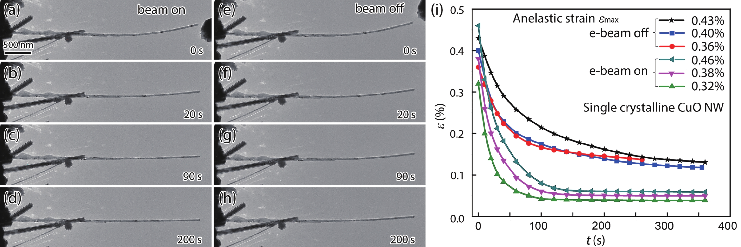
Cheng G M, Miao C Y, Qin Q Q, et al. Large anelasticity and associated energy dissipation in single-crystalline nanowires. Nat Nanotech, 2015, 10, 687 doi: 10.1038/nnano.2015.135 |
| [69] |
Li L, Chen G, Zheng H, et al. Room-temperature oxygen vacancy migration induced reversible phase transformation during the anelastic deformation in CuO. Nat Commun, 2021, 12, 3863 doi: 10.1038/s41467-021-24155-z |
| [70] |
Sun X, Zhu W, Wu D, et al. Surface-reaction induced structural oscillations in the subsurface. Nat Commun, 2020, 11, 305 doi: 10.1038/s41467-019-14167-1 |
| [71] |
|
| [72] |
Freeman C L, Claeyssens F, Allan N L, et al. Graphitic nanofilms as precursors to wurtzite films: theory. Phys Rev Lett, 2006, 96, 066102 doi: 10.1103/PhysRevLett.96.066102 |
| [73] |
Morgan B J. First-principles study of epitaxial strain as a method of B4→BCT stabilization in ZnO, ZnS, and CdS. Phys Rev B, 2010, 82, 153408 doi: 10.1103/PhysRevB.82.153408 |
| [74] |
Jeannin M, Artioli A, Rueda-Fonseca P, et al. Light-hole exciton in a nanowire quantum dot. Phys Rev B, 2017, 95, 035305 doi: 10.1103/PhysRevB.95.035305 |
| [75] |
Sponza L, Goniakowski J, Noguera C. Confinement effects in ultrathin ZnO polymorph films: electronic and optical properties. Phys Rev B, 2016, 93, 195435 doi: 10.1103/PhysRevB.93.195435 |
| [76] |
Yamamoto S, Mishina T. Observation of dark exciton luminescence from ZnO nanocrystals in the quantum confinement regime. Phys Rev B, 2011, 83, 165435 doi: 10.1103/PhysRevB.83.165435 |
| [77] |
Zhao X, Wei C M, Yang L, et al. Quantum confinement and electronic properties of silicon nanowires. Phys Rev Lett, 2004, 92, 236805 doi: 10.1103/PhysRevLett.92.236805 |
| [78] |
Liu B H, Mcbriarty M E, Bedzyk M J, et al. Structural transformations of zinc oxide layers on Pt(111). J Phys Chem C, 2014, 118, 28725 doi: 10.1021/jp510069q |
| [79] |
Deng X Y, Yao K, Sun K J, et al. Growth of single- and bilayer ZnO on Au(111) and interaction with copper. J Phys Chem C, 2013, 246, 11211 doi: 10.1021/jp402008w |
| [80] |
Weirum G, Barcaro G, Fortunelli A, et al. Growth and surface structure of zinc oxide layers on a Pd(111) surface. J Phys Chem C, 2010, 114, 15432 doi: 10.1021/jp104620n |
| [81] |
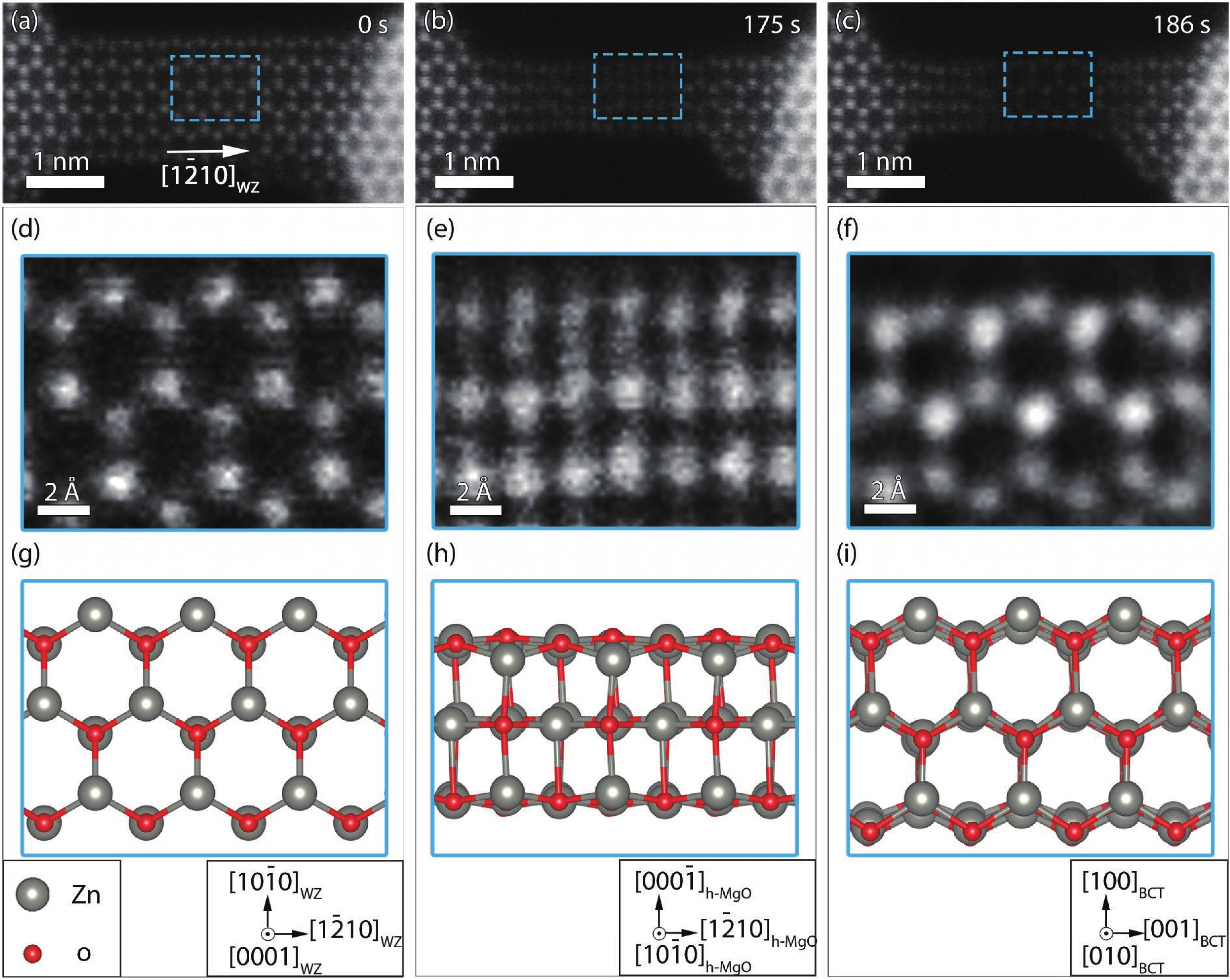
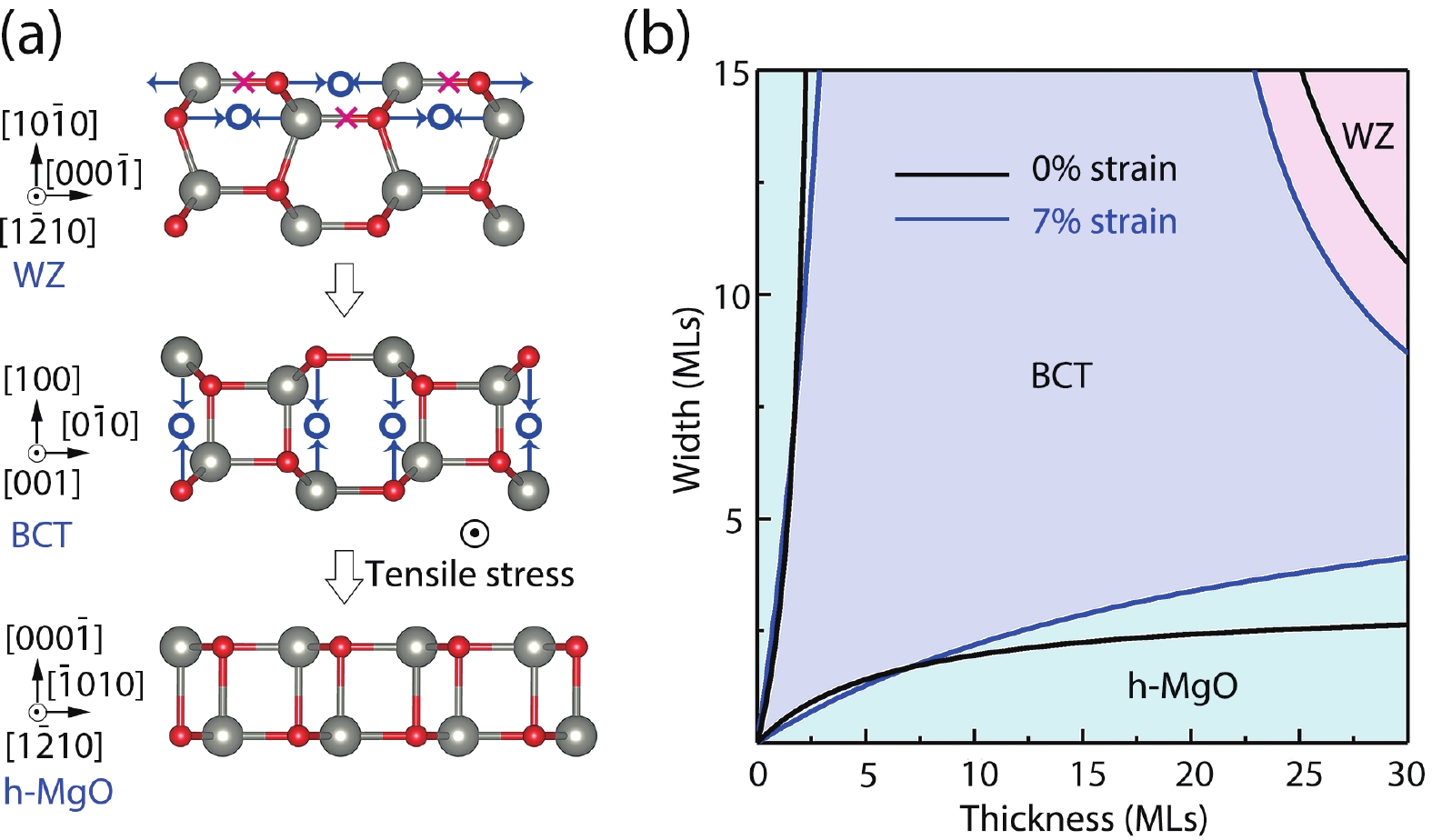
Zhao P L, Guan X X, Zheng H, et al. Surface- and strain-mediated reversible phase transformation in quantum-confined ZnO nanowires. Phys Rev Lett, 2019, 123, 216101 doi: 10.1103/PhysRevLett.123.216101 |
| [82] |
Kulkarni A J, Zhou M, Sarasamak K, et al. Novel phase transformation in ZnO nanowires under tensile loading. Phys Rev Lett, 2006, 97, 105502 doi: 10.1103/PhysRevLett.97.105502 |
| [83] |
Wang J, Kulkarni A J, Sarasamak K, et al. Molecular dynamics and density functional studies of a body-centered-tetragonal polymorph of ZnO. Phys Rev B, 2007, 76, 172103 doi: 10.1103/PhysRevB.76.172103 |
| [84] |
|
| [85] |
|
| [86] |
Susi T, Meyer J C, Kotakoski J. Quantifying transmission electron microscopy irradiation effects using two-dimensional materials. Nat Rev Phys, 2019, 1, 397 doi: 10.1038/s42254-019-0058-y |
| [87] |
Lee S B. Rocksalt ZnO nanocrystal formation by beam irradiation of wurtzite ZnO in a transmission electron microscope. Physica E, 2016, 84, 310 doi: 10.1016/j.physe.2016.07.001 |
| [88] |
Zhao L L, Li L, Sheng H P, et al. Atomistic insight into ordered defect superstructures at novel grain boundaries in CuO nanosheets: From structures to electronic properties. Nano Res, 2019, 12, 1099 doi: 10.1007/s12274-019-2354-3 |
| [89] |
Jia S F, Li L, Zhao L L, et al. Surface-dependent formation of Zn clusters in ZnO single crystals by electron irradiation. Phys Rev Mater, 2018, 2, 060402 doi: 10.1103/PhysRevMaterials.2.060402 |
| [90] |
Look D C, Hemsky J W, Sizelove J R. Residual native shallow donor in ZnO. Phys Rev Lett, 1999, 82, 2552 doi: 10.1103/PhysRevLett.82.2552 |
| [91] |
Coskun C, Look D C, Farlow G C, et al. Radiation hardness of ZnO at low temperatures. Semicond Sci Technol, 2004, 19, 752 doi: 10.1088/0268-1242/19/6/016 |
| [92] |
Kucheyev S O, Jagadish C, Williams J S, et al. Implant isolation of ZnO. J Appl Phys, 2003, 93, 2972 doi: 10.1063/1.1542939 |
| [93] |
Ooe K, Seki T, Ikuhara Y, et al. High contrast STEM imaging for light elements by an annular segmented detector. Ultramicroscopy, 2019, 202, 148 doi: 10.1016/j.ultramic.2019.04.011 |
| [94] |
Ishikawa R, Findlay S D, Seki T, et al. Direct electric field imaging of graphene defects. Nat Commun, 2018, 9, 3878 doi: 10.1038/s41467-018-06387-8 |
| [95] |
Shibata N, Findlay S D, Kohno Y, et al. Differential phase-contrast microscopy at atomic resolution. Nat Phys, 2012, 8, 611 doi: 10.1038/nphys2337 |
| [96] |
Lee T, Mas'ud F A, Kim M J, et al. Spatially resolved Raman spectroscopy of defects, strains, and strain fluctuations in domain structures of monolayer graphene. Sci Rep, 2017, 7, 16681 doi: 10.1038/s41598-017-16969-z |
| [97] |
Huang M, Yan H, Heinz T F, et al. Probing strain-induced electronic structure change in graphene by Raman spectroscopy. Nano Lett, 2010, 10, 4074 doi: 10.1021/nl102123c |
| [98] |
Dennett C A, Hua Z, Khanolkar A, et al. The influence of lattice defects, recombination, and clustering on thermal transport in single crystal thorium dioxide. APL Mater, 2020, 8, 111103 doi: 10.1063/5.0025384 |


 DownLoad: