ARTICLES

Sub-bandgap refractive indexes and optical properties of Si-doped β-Ga2O3 semiconductor thin films

Yitian Bao1, Xiaorui Wang1 and Shijie Xu1, 2,

+ Author Affiliations

 Corresponding author: Shijie Xu, xusj@fudan.edu.cn; sjxu@hku.hk

PDF

Turn off MathJax

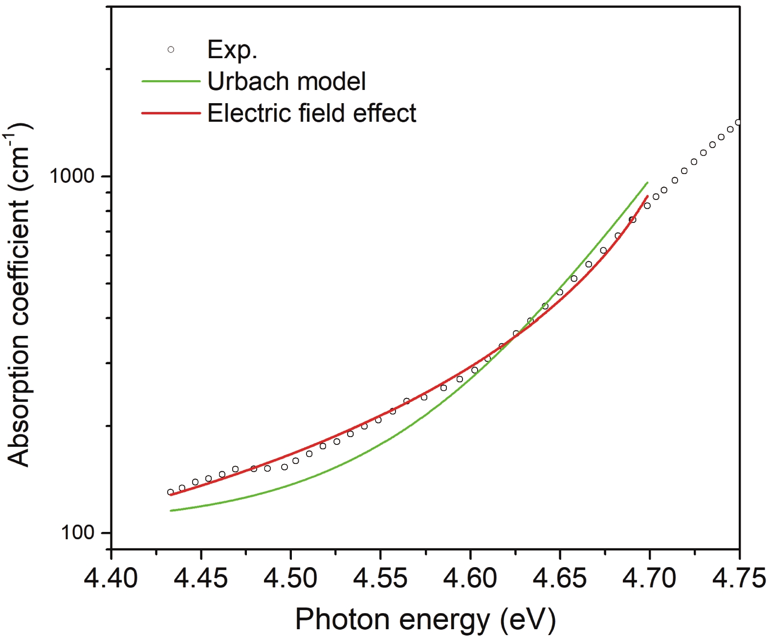
Abstract: In this article, we present a theoretical study on the sub-bandgap refractive indexes and optical properties of Si-doped β-Ga2O3 thin films based on newly developed models. The measured sub-bandgap refractive indexes of β-Ga2O3 thin film are explained well with the new model, leading to the determination of an explicit analytical dispersion of refractive indexes for photon energy below an effective optical bandgap energy of 4.952 eV for the β-Ga2O3 thin film. Then, the oscillatory structures in long wavelength regions in experimental transmission spectra of Si-doped β-Ga2O3 thin films with different Si doping concentrations are quantitively interpreted utilizing the determined sub-bandgap refractive index dispersion. Meanwhile, effective optical bandgap values of Si-doped β-Ga2O3 thin films are further determined and are found to decrease with increasing the Si doping concentration as expectedly. In addition, the sub-bandgap absorption coefficients of Si-doped β-Ga2O3 thin film are calculated under the frame of the Franz–Keldysh mechanism due to the electric field effect of ionized Si impurities. The theoretical absorption coefficients agree with the available experimental data. These key parameters obtained in the present study may enrich the present understanding of the sub-bandgap refractive indexes and optical properties of impurity-doped β-Ga2O3 thin films.

Key words: gallium oxidesub-bandgap refractive indexSi dopingeffective optical bandgapsub-bandgap absorption


[1]
Pearton S J, Yang J, Cary IV P H, et al. A review of Ga2O3 materials, processing, and device. Appl Phys Rev, 2018, 5, 011301 doi: 10.1063/1.5006941
[2]
Mohamed H F, Xia C, Sai Q, et al. Growth and fundamentals of bulk β-Ga2O3 single crystals. J Semicond, 2019, 40, 011801 doi: 10.1088/1674-4926/40/1/011801
[3]
Zhang F, Arita M, Wang X, et al. Toward controlling the carrier density of Si doped Ga2O3 films by pulsed laser deposition. Appl Phys Lett, 2016, 109, 102105 doi: 10.1063/1.4962463
[4]
Hu D, Wang Y, Zhuang S, et al. Surface morphology evolution and optoelectronic properties of heteroepitaxial Si-doped β-Ga2O3 thin films grown by metal-organic chemical vapor deposition. Ceram Internation, 2018, 44, 3122 doi: 10.1016/j.ceramint.2017.11.079
[5]
Pearton S J, Ren F, Tadjer M, et al. Perspective: Ga2O3 for ultra-high power rectifiers and MOSFETS. J Appl Phys, 2018, 124, 220901 doi: 10.1063/1.5062841
[6]
Yang J, Ahn S, Ren F, et al. High breakdown voltage (−201) β-Ga2O3 Schottky rectifiers. IEEE Electron Device Lett, 2017, 38, 906 doi: 10.1109/LED.2017.2703609
[7]
Wang B, Xiao M, Yan X, et al. High-voltage vertical Ga2O3 power rectifiers operational at high temperatures up to 600 K. Appl Phys Lett, 2019, 115, 263503 doi: 10.1063/1.5132818
[8]
Chabak K D, McCandless J P, Moser N A, et al. Recessed-gate enhancement-mode β-Ga2O3 MOSFETs. IEEE Electron Device Lett, 2018, 39, 67 doi: 10.1109/LED.2017.2779867
[9]
Green A J, Chabak K D, Baldini M, et al. β-Ga2O3 MOSFETs for radio frequency operation. IEEE Electron Device Lett, 2017, 38, 790 doi: 10.1109/LED.2017.2694805
[10]
Moser N, McCandless J, Crespo A, et al. Ge-doped β-Ga2O3 MOSFETs. IEEE Electron Device Lett, 2017, 38, 775 doi: 10.1109/LED.2017.2697359
[11]
Oh S, Kim C K, Kim J. High responsivity β-Ga2O3 metal–semiconductor–metal solar-blind photodetectors with ultraviolet transparent graphene electrodes. ACS Photon, 2018, 5, 1123 doi: 10.1021/acsphotonics.7b01486
[12]
Chen Y C, Lu Y J, Liu Q, et al. Ga2O3 photodetector arrays for solar-blind imaging. J Mater Chem C, 2019, 7, 2557 doi: 10.1039/C8TC05251D
[13]
Xu J, Zheng W, Huang F. Gallium oxide solar-blind ultraviolet photodetectors: a review. J Mater Chem C, 2019, 7, 8753 doi: 10.1039/C9TC02055A
[14]
Liu Z, Wang X, Liu Y, et al. A high-performance ultraviolet solar-blind photodetector based on a β-Ga2O3 Schottky photodiode. J Mater Chem C, 2019, 7, 13920 doi: 10.1039/C9TC04912F
[15]
Zhang L, Xiu X, Li Y, et al. Solar-blind ultraviolet photodetector based on vertically aligned single-crystalline β-Ga2O3 nanowire arrays. Nanophotonics, 2020, 9, 0295 doi: 10.1515/nanoph-2019-0336
[16]
Xie C, Lu X, Liang Y, et al. Patterned growth of β-Ga2O3 thin films for solar-blind deep-ultraviolet photodetectors array and optical imaging application. J Mater Sci Technol, 2021, 72, 189 doi: 10.1016/j.jmst.2020.09.015
[17]
Rebien M, Henrion W, Hong M, et al. Optical properties of gallium oxide thin films. Appl Phys Lett, 2002, 81, 250 doi: 10.1063/1.1491613
[18]
Bao Y, Xu S. Variable-period oscillations in optical spectra in sub-bandgap long wavelength region: Signatures of new dispersion of refractive index. J Phys D, 2021, 54, 155102 doi: 10.1088/1361-6463/abd6d4
[19]
Bhaumik I, Bhatt R, Ganesamoorthy S, et al. Temperature-dependent index of refraction of monoclinic Ga2O3 single crystal. Appl Opt, 2011, 50, 6006 doi: 10.1364/AO.50.006006
[20]
Ueda N, Hosono H, Waseda R, et al. Anisotropy of electrical and optical properties in β-Ga2O3 single crystals. Appl Phys Lett, 1997, 71, 933 doi: 10.1063/1.119693
[21]
Hilfiker M, Kilic U, Mock A, et al. Dielectric function tensor (1.5 eV to 9.0 eV), anisotropy, and band to band transitions of monoclinic β-(Al xGa1– x)2O3 (x ≤ 0.21) films. Appl Phys Lett, 2019, 114, 231901 doi: 10.1063/1.5097780
[22]
Furthmüller J, Bechstedt F. Quasiparticle bands and spectra of Ga2O3 polymorphs. Phys Rev B, 2016, 93, 115204 doi: 10.1103/PhysRevB.93.115204
[23]
Yan J, Qu C. Electronic structure and optical properties of F-doped-Ga2O3 from first principles calculations. J Semicond, 2016, 37, 042002 doi: 10.1088/1674-4926/37/4/042002
[24]
Mock A, Korlacki R, Briley C, et al. Band-to-band transitions, selection rules, effective mass, and excitonic contributions in monoclinic β-Ga2O3. Phys Rev B, 2017, 96, 245205 doi: 10.1103/PhysRevB.96.245205
[25]
Galazka Z. β-Ga2O3 for wide-bandgap electronics and optoelectronics. Semicond Sci Technol, 2018, 33, 113001 doi: 10.1088/1361-6641/aadf78
[26]
Redfield D. Effect of defect fields on the optical absorption edge. Phys Rev, 1963, 130, 916 doi: 10.1103/PhysRev.130.916
[27]
Tharmalingam K. Optical absorption in the presence of a uniform field. Phys Rev, 1963, 130, 2204 doi: 10.1103/PhysRev.130.2204
[28]
Bao Y, Xu S. Dopant-induced electric fields and their influence on the band-edge absorption of GaN. ACS Omega, 2019, 4, 15401 doi: 10.1021/acsomega.9b01394
[29]
Rafique S, Han L, Mou S, et al. Temperature and doping concentration dependence of the energy band gap in β-Ga2O3 thin films grown on sapphire. Opt Mater Express, 2017, 7, 3561 doi: 10.1364/OME.7.003561
[30]
Subrina R, Han L, Zhao H. Synthesis of wide bandgap Ga2O3 (Eg ~ 4.6–4.7 eV) thin films on sapphire by low pressure chemical vapor deposition. Phys Status Solidi A, 2016, 213, 1002 doi: 10.1002/pssa.201532711
[31]
Zhang J, Shi J, Qi D C, et al. Recent progress on the electronic structure, defect, and doping properties of Ga2O3. APL Mater, 2020, 8, 020906 doi: 10.1063/1.5142999
[32]
Peelaers H, Van de Walle C G. Sub-band-gap absorption in Ga2O3. Appl Phys Lett, 2017, 111, 182104 doi: 10.1063/1.5001323
[33]
Bechstedt F, Furthmüller J. Influence of screening dynamics on excitons in Ga2O3 polymorphs. Appl Phys Lett, 2019, 114, 122101 doi: 10.1063/1.5084324
[34]
Guo R, Su J, Yuan H, et al. Surface functionalization modulates the structural and optoelectronic properties of two-dimensional Ga2O3. Mater Today Phys, 2020, 12, 100192 doi: 10.1016/j.mtphys.2020.100192
[35]
Shi S L, Xu S J. Determination of effective mass of heavy hole from phonon-assisted excitonic luminescence spectra in ZnO. J Appl Phys, 2011, 109, 053510 doi: 10.1063/1.3549724
[36]
Wang X, Yu D, Xu S. Determination of absorption coefficients and Urbach tail depth of ZnO below the bandgap with two-photon photoluminescence. Opt Express, 2020, 28, 13817 doi: 10.1364/OE.391534
[37]
Ye H G, Su Z C, Tang F, et al. Role of free electrons in phosphorescence in n-type wide bandgap semiconductors. Phys Chem Chem Phys, 2017, 19, 30332 doi: 10.1039/C7CP05796B
[38]
Ye H, Su Z, Tang F, et al. Probing defects in ZnO by persistent phosphorescence. Opto-Electron Adv, 2018, 1, 180011 doi: 10.29026/oea.2018.180011
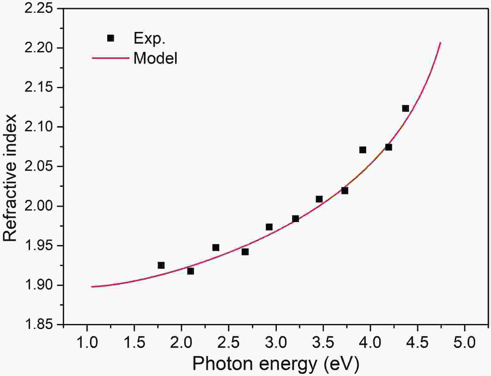
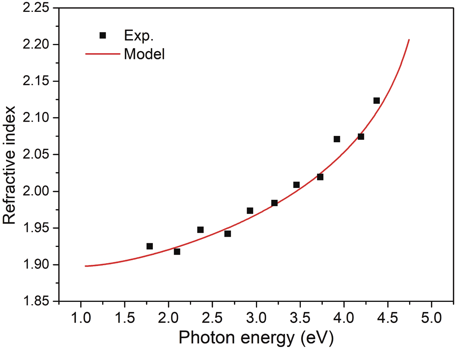
Fig. 1.  (Color online) The experimental (solid squares) and calculated (solid line) refractive indexes of β-Ga2O3 thin film as a function of photon energy. The experimental data were from Ref. [17], while the solid line was fitted with Eq. (1).

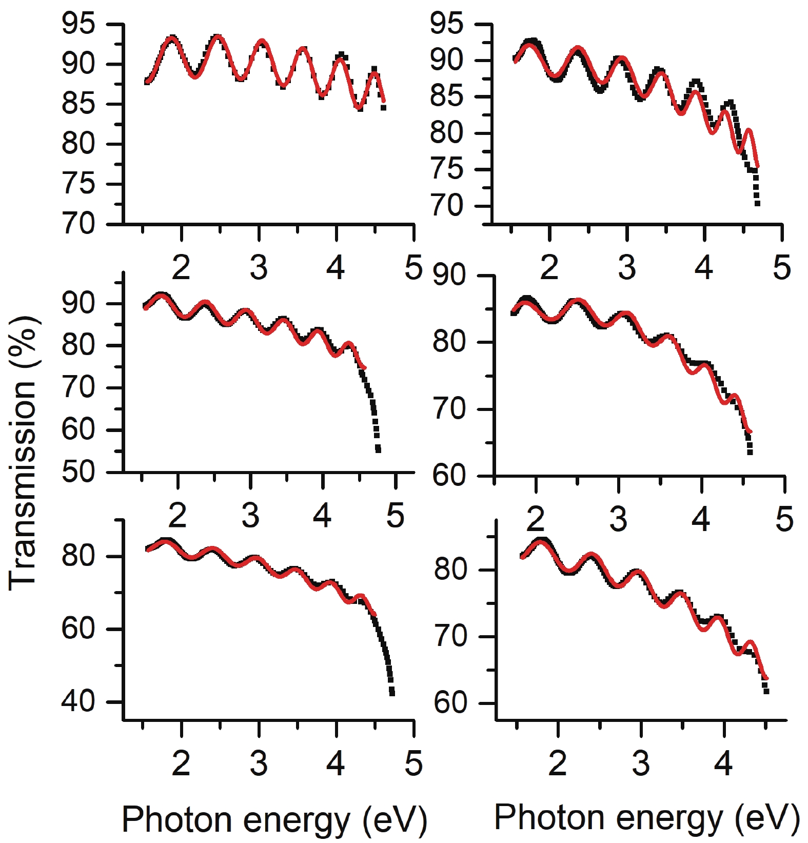
Fig. 2.  (Color online) The measured transmission spectra (solid squares) and corresponding fitting curves (red solid lines) of the β-Ga2O3 thin films. The experimental spectra were measured by Hu et al.[4], while the fitting curves were obtained with Eq. (2) described in the text.

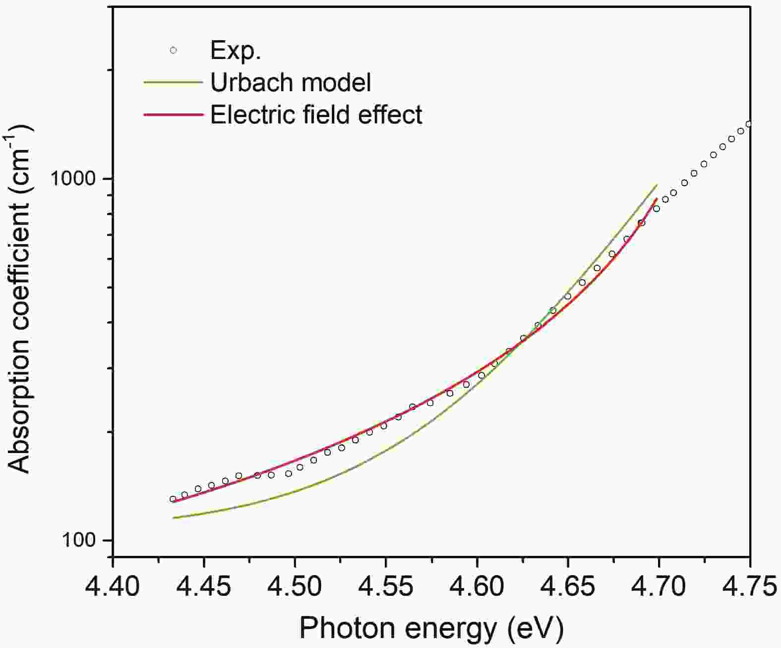
Fig. 3.  (Color online) Measured (open circles) and calculated (solid lines) sub-bandgap absorption coefficients of β-Ga2O3 thin film with an impurity density of 2.52 × 1024 m–3. Note that the plot is drawn in a semi-logarithmic scale. The original experimental data was from Ref. [29].

Table 1.   Determined effective optical bandgap values vs. flow rates of SiH4.

Sampleabcdefg
Effective bandgap (eV)4.9524.9234.9204.9184.8654.8234.770
Flow rates of SiH4
(sccm)
0.000.020.040.080.120.160.20
DownLoad: CSV
[1]
Pearton S J, Yang J, Cary IV P H, et al. A review of Ga2O3 materials, processing, and device. Appl Phys Rev, 2018, 5, 011301 doi: 10.1063/1.5006941
[2]
Mohamed H F, Xia C, Sai Q, et al. Growth and fundamentals of bulk β-Ga2O3 single crystals. J Semicond, 2019, 40, 011801 doi: 10.1088/1674-4926/40/1/011801
[3]
Zhang F, Arita M, Wang X, et al. Toward controlling the carrier density of Si doped Ga2O3 films by pulsed laser deposition. Appl Phys Lett, 2016, 109, 102105 doi: 10.1063/1.4962463
[4]
Hu D, Wang Y, Zhuang S, et al. Surface morphology evolution and optoelectronic properties of heteroepitaxial Si-doped β-Ga2O3 thin films grown by metal-organic chemical vapor deposition. Ceram Internation, 2018, 44, 3122 doi: 10.1016/j.ceramint.2017.11.079
[5]
Pearton S J, Ren F, Tadjer M, et al. Perspective: Ga2O3 for ultra-high power rectifiers and MOSFETS. J Appl Phys, 2018, 124, 220901 doi: 10.1063/1.5062841
[6]
Yang J, Ahn S, Ren F, et al. High breakdown voltage (−201) β-Ga2O3 Schottky rectifiers. IEEE Electron Device Lett, 2017, 38, 906 doi: 10.1109/LED.2017.2703609
[7]
Wang B, Xiao M, Yan X, et al. High-voltage vertical Ga2O3 power rectifiers operational at high temperatures up to 600 K. Appl Phys Lett, 2019, 115, 263503 doi: 10.1063/1.5132818
[8]
Chabak K D, McCandless J P, Moser N A, et al. Recessed-gate enhancement-mode β-Ga2O3 MOSFETs. IEEE Electron Device Lett, 2018, 39, 67 doi: 10.1109/LED.2017.2779867
[9]
Green A J, Chabak K D, Baldini M, et al. β-Ga2O3 MOSFETs for radio frequency operation. IEEE Electron Device Lett, 2017, 38, 790 doi: 10.1109/LED.2017.2694805
[10]
Moser N, McCandless J, Crespo A, et al. Ge-doped β-Ga2O3 MOSFETs. IEEE Electron Device Lett, 2017, 38, 775 doi: 10.1109/LED.2017.2697359
[11]
Oh S, Kim C K, Kim J. High responsivity β-Ga2O3 metal–semiconductor–metal solar-blind photodetectors with ultraviolet transparent graphene electrodes. ACS Photon, 2018, 5, 1123 doi: 10.1021/acsphotonics.7b01486
[12]
Chen Y C, Lu Y J, Liu Q, et al. Ga2O3 photodetector arrays for solar-blind imaging. J Mater Chem C, 2019, 7, 2557 doi: 10.1039/C8TC05251D
[13]
Xu J, Zheng W, Huang F. Gallium oxide solar-blind ultraviolet photodetectors: a review. J Mater Chem C, 2019, 7, 8753 doi: 10.1039/C9TC02055A
[14]
Liu Z, Wang X, Liu Y, et al. A high-performance ultraviolet solar-blind photodetector based on a β-Ga2O3 Schottky photodiode. J Mater Chem C, 2019, 7, 13920 doi: 10.1039/C9TC04912F
[15]
Zhang L, Xiu X, Li Y, et al. Solar-blind ultraviolet photodetector based on vertically aligned single-crystalline β-Ga2O3 nanowire arrays. Nanophotonics, 2020, 9, 0295 doi: 10.1515/nanoph-2019-0336
[16]
Xie C, Lu X, Liang Y, et al. Patterned growth of β-Ga2O3 thin films for solar-blind deep-ultraviolet photodetectors array and optical imaging application. J Mater Sci Technol, 2021, 72, 189 doi: 10.1016/j.jmst.2020.09.015
[17]
Rebien M, Henrion W, Hong M, et al. Optical properties of gallium oxide thin films. Appl Phys Lett, 2002, 81, 250 doi: 10.1063/1.1491613
[18]
Bao Y, Xu S. Variable-period oscillations in optical spectra in sub-bandgap long wavelength region: Signatures of new dispersion of refractive index. J Phys D, 2021, 54, 155102 doi: 10.1088/1361-6463/abd6d4
[19]
Bhaumik I, Bhatt R, Ganesamoorthy S, et al. Temperature-dependent index of refraction of monoclinic Ga2O3 single crystal. Appl Opt, 2011, 50, 6006 doi: 10.1364/AO.50.006006
[20]
Ueda N, Hosono H, Waseda R, et al. Anisotropy of electrical and optical properties in β-Ga2O3 single crystals. Appl Phys Lett, 1997, 71, 933 doi: 10.1063/1.119693
[21]
Hilfiker M, Kilic U, Mock A, et al. Dielectric function tensor (1.5 eV to 9.0 eV), anisotropy, and band to band transitions of monoclinic β-(Al xGa1– x)2O3 (x ≤ 0.21) films. Appl Phys Lett, 2019, 114, 231901 doi: 10.1063/1.5097780
[22]
Furthmüller J, Bechstedt F. Quasiparticle bands and spectra of Ga2O3 polymorphs. Phys Rev B, 2016, 93, 115204 doi: 10.1103/PhysRevB.93.115204
[23]
Yan J, Qu C. Electronic structure and optical properties of F-doped-Ga2O3 from first principles calculations. J Semicond, 2016, 37, 042002 doi: 10.1088/1674-4926/37/4/042002
[24]
Mock A, Korlacki R, Briley C, et al. Band-to-band transitions, selection rules, effective mass, and excitonic contributions in monoclinic β-Ga2O3. Phys Rev B, 2017, 96, 245205 doi: 10.1103/PhysRevB.96.245205
[25]
Galazka Z. β-Ga2O3 for wide-bandgap electronics and optoelectronics. Semicond Sci Technol, 2018, 33, 113001 doi: 10.1088/1361-6641/aadf78
[26]
Redfield D. Effect of defect fields on the optical absorption edge. Phys Rev, 1963, 130, 916 doi: 10.1103/PhysRev.130.916
[27]
Tharmalingam K. Optical absorption in the presence of a uniform field. Phys Rev, 1963, 130, 2204 doi: 10.1103/PhysRev.130.2204
[28]
Bao Y, Xu S. Dopant-induced electric fields and their influence on the band-edge absorption of GaN. ACS Omega, 2019, 4, 15401 doi: 10.1021/acsomega.9b01394
[29]
Rafique S, Han L, Mou S, et al. Temperature and doping concentration dependence of the energy band gap in β-Ga2O3 thin films grown on sapphire. Opt Mater Express, 2017, 7, 3561 doi: 10.1364/OME.7.003561
[30]
Subrina R, Han L, Zhao H. Synthesis of wide bandgap Ga2O3 (Eg ~ 4.6–4.7 eV) thin films on sapphire by low pressure chemical vapor deposition. Phys Status Solidi A, 2016, 213, 1002 doi: 10.1002/pssa.201532711
[31]
Zhang J, Shi J, Qi D C, et al. Recent progress on the electronic structure, defect, and doping properties of Ga2O3. APL Mater, 2020, 8, 020906 doi: 10.1063/1.5142999
[32]
Peelaers H, Van de Walle C G. Sub-band-gap absorption in Ga2O3. Appl Phys Lett, 2017, 111, 182104 doi: 10.1063/1.5001323
[33]
Bechstedt F, Furthmüller J. Influence of screening dynamics on excitons in Ga2O3 polymorphs. Appl Phys Lett, 2019, 114, 122101 doi: 10.1063/1.5084324
[34]
Guo R, Su J, Yuan H, et al. Surface functionalization modulates the structural and optoelectronic properties of two-dimensional Ga2O3. Mater Today Phys, 2020, 12, 100192 doi: 10.1016/j.mtphys.2020.100192
[35]
Shi S L, Xu S J. Determination of effective mass of heavy hole from phonon-assisted excitonic luminescence spectra in ZnO. J Appl Phys, 2011, 109, 053510 doi: 10.1063/1.3549724
[36]
Wang X, Yu D, Xu S. Determination of absorption coefficients and Urbach tail depth of ZnO below the bandgap with two-photon photoluminescence. Opt Express, 2020, 28, 13817 doi: 10.1364/OE.391534
[37]
Ye H G, Su Z C, Tang F, et al. Role of free electrons in phosphorescence in n-type wide bandgap semiconductors. Phys Chem Chem Phys, 2017, 19, 30332 doi: 10.1039/C7CP05796B
[38]
Ye H, Su Z, Tang F, et al. Probing defects in ZnO by persistent phosphorescence. Opto-Electron Adv, 2018, 1, 180011 doi: 10.29026/oea.2018.180011
  • Search

    Advanced Search >>

    GET CITATION

    shu

    Export: BibTex EndNote

    Article Metrics

    Article views: 1372 Times PDF downloads: 130 Times Cited by: 0 Times

    History

    Received: 01 December 2021 Revised: 19 January 2022 Online: Accepted Manuscript: 11 April 2022Uncorrected proof: 15 April 2022Published: 06 June 2022

    Catalog

      Email This Article

      User name:
      Email:*请输入正确邮箱
      Code:*验证码错误
      Yitian Bao, Xiaorui Wang, Shijie Xu. Sub-bandgap refractive indexes and optical properties of Si-doped β-Ga2O3 semiconductor thin films[J]. Journal of Semiconductors, 2022, 43(6): 062802. doi: 10.1088/1674-4926/43/6/062802 Y T Bao, X R Wang, S J Xu. Sub-bandgap refractive indexes and optical properties of Si-doped β-Ga2O3 semiconductor thin films[J]. J. Semicond, 2022, 43(6): 062802. doi: 10.1088/1674-4926/43/6/062802Export: BibTex EndNote
      Citation:
      Yitian Bao, Xiaorui Wang, Shijie Xu. Sub-bandgap refractive indexes and optical properties of Si-doped β-Ga2O3 semiconductor thin films[J]. Journal of Semiconductors, 2022, 43(6): 062802. doi: 10.1088/1674-4926/43/6/062802

      Y T Bao, X R Wang, S J Xu. Sub-bandgap refractive indexes and optical properties of Si-doped β-Ga2O3 semiconductor thin films[J]. J. Semicond, 2022, 43(6): 062802. doi: 10.1088/1674-4926/43/6/062802
      Export: BibTex EndNote

      Sub-bandgap refractive indexes and optical properties of Si-doped β-Ga2O3 semiconductor thin films

      doi: 10.1088/1674-4926/43/6/062802
      More Information
      • Author Bio:

        Yitian Bao got his PhD and MPhil degrees from the Department of Physics, the University of Hong Kong, and a BS degree from the Department of Math, Fudan University. His current research interests include deep learning, luminescence mechanism and material science

        Xiaorui Wang is a current postgraduate student at the Department of Physics, the University of Hong Kong (HKU). He received his BSc and MEng degrees in 2014 and 2017 respectively at HIT. His current research interests include luminescent material science, and laser engineering and science

        Shijie Xu is a tenured professor in Department of Physics, the University of Hong Kong, and a distinguished professor in Department of Optical Science and Engineering, Fudan University. He earned his PhD degree in Electronic Engineering from Xi’an Jiaotong University in 1993. His current research interests include many-body quantum and localized-states ensemble (LSE) luminescence mechanisms in solids, especially in wide bandgap semiconductors and their nanostructures. He and his PhD students have developed LSE luminescence model which has been widely cited and recognized, including citations in the updated editions of two classic textbooks, Semiconductor Optics (C.F. Klingshirn, Springer) and The Physics of Semiconductors (M. Grundmann, Springer)

      • Corresponding author: xusj@fudan.edu.cn; sjxu@hku.hk
      • Received Date: 2021-12-01
      • Revised Date: 2022-01-19
      • Available Online: 2022-04-11

      Catalog

        /

        DownLoad:  Full-Size Img  PowerPoint
        Return
        Return