


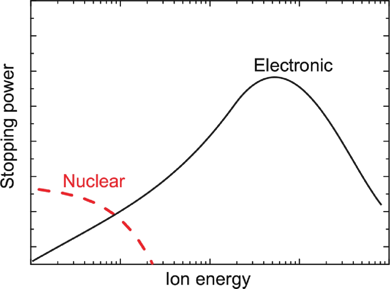
Fig. 1.
(Color online) Schematic of the cross-section for electronic and nuclear stopping processes as a function of ion energy[12].
REVIEWS
Ye Yuan1, , Shengqiang Zhou2 and Xinqiang Wang1, 3,
Corresponding author: Ye Yuan, yuanye@sslab.org.cn; Xinqiang Wang, wangshi@pku.edu.cn
Abstract: In this review, the application of light ion irradiation is discussed for tailoring novel functional materials and for improving the performance in SiC or Si based electrical power devices. The deep traps and electronic disorder produced by light ion irradiation can modify the electrical, magnetic, and optical properties of films (e.g., dilute ferromagnetic semiconductors and topological materials). Additionally, benefiting from the high reproducibility, precise manipulation of functional depth and density of defects, as well as the flexible patternability, the helium or proton ion irradiation has been successfully employed in improving the dynamic performance of SiC and Si based PiN diode power devices by reducing their majority carrier lifetime, although the static performance is sacrificed due to deep level traps. Such a trade-off has been regarded as the key point to compromise the static and dynamic performances of power devices. As a result, herein the light ion irradiation is highlighted in both exploring new physics and optimizing the performance in functional materials and electrical devices.
Key words: ion irradiation, power device, crystal, thin film, functional materials
| [1] |
Mayer J, Marsh O. Ion implantation in semiconductors. Appl Solid State Sci, 1969, 1, 239 doi: 10.1016/S0065-2539(08)60539-9
|
| [2] |
Stephen J, Dearnaley G, Freeman J H, et al. Ion implantation. Book Review, 1973
|
| [3] |
Yuan Y, Xu C, Hübner R, et al. Interplay between localization and magnetism in (Ga, Mn)As and (In, Mn)As. Phys Rev Mater, 2017, 1, 054401 doi: 10.1103/PhysRevMaterials.1.054401
|
| [4] |
Yuan Y, Wang Y, Khalid M, et al. Ferromagnetic GaMnP prepared by ion implantation and pulsed laser annealing. IEEE Trans Mag, 2014, 50, 2401304 doi: 10.1109/TMAG.2014.2322332
|
| [5] |
Yuan Y, Wang M, Xu C, et al. Electronic phase separation in insulating (Ga, Mn)As with low compensation: Super-paramagnetism and hopping conduction. J Phys Condens Matter, 2018, 30, 095801 doi: 10.1088/1361-648X/aaa9a7
|
| [6] |
Yuan Y, Hübner R, Liu F, et al. Ferromagnetic Mn-implanted GaP: Microstructures vs magnetic properties. ACS Appl Mater & Interfaces, 2016, 8, 3912 doi: 10.1021/acsami.5b10949
|
| [7] |
Yuan Y, Wang Y, Gao K, et al. High Curie temperature and perpendicular magnetic anisotropy in homoepitaxial InMnAs films. J Phys D, 2015, 48, 235002 doi: 10.1088/0022-3727/48/23/235002
|
| [8] |
Prucnal S, Heera V, Hübner R, et al. Superconductivity in single-crystalline aluminum- and gallium-hyperdoped germanium. Phys Rev Mater, 2019, 3, 054802 doi: 10.1103/PhysRevMaterials.3.054802
|
| [9] |
Wang M, Berencén Y, García-Hemme E, et al. Extended infrared photoresponse in Te-hyperdoped Si at room temperature. Phys Rev Appl, 2018, 10, 024054 doi: 10.1103/PhysRevApplied.10.024054
|
| [10] |
Liu F, Prucnal S, Berencén Y, et al. Realizing the insulator-to-metal transition in Se-hyperdoped Si via non-equilibrium material processing. J Phys D, 2017, 50, 415102 doi: 10.1088/1361-6463/aa82f9
|
| [11] |
Ziegler J F, Ziegler M D, Biersack J B. SRIM-The stopping and range of ions in matter (2010). Nucl Instrum Methods Phys Res Sect B, 2010, 268, 1818 doi: 10.1016/j.nimb.2010.02.091
|
| [12] |
Zhou S, Chen X L. Defect-induced magnetism in SiC. J Phys D, 2019, 52, 393001 doi: 10.1088/1361-6463/ab2495
|
| [13] |
Lee P A, Ramakrishnan T V. Disordered electronic systems. Rev Mod Phys, 1985, 57, 287 doi: 10.1103/RevModPhys.57.287
|
| [14] |
Pantelides S T. The electronic structure of impurities and other point defects in semiconductors. Rev Mod Phys, 1978, 50, 797 doi: 10.1103/RevModPhys.50.797
|
| [15] |
Park J, Choi J H, Kong K, et al. Electrically driven mid-submicrometre pixelation of InGaN micro-light-emitting diode displays for augmented-reality glasses. Nat Photonics, 2021, 15, 449 doi: 10.1038/s41566-021-00783-1
|
| [16] |
Zhou S, Li L, Yuan Y, et al. Precise tuning of the Curie temperature of (Ga, Mn)As-based magnetic semiconductors by hole compensation: Support for valence-band ferromagnetism. Phy Rev B, 2016, 94, 075205 doi: 10.1103/PhysRevB.94.075205
|
| [17] |
Xu C, Wang M, Yuan Y, et al. Hole compensation effect in III-Mn-V dilute ferromagnetic semiconductors. J Phys D, 2019, 52, 355301 doi: 10.1088/1361-6463/ab25dd
|
| [18] |
Rischau C W, Leridon B, Fauqué B, et al. Doping of Bi2Te3 using electron irradiation. Phys Rev B, 2013, 88, 205207 doi: 10.1103/PhysRevB.88.205207
|
| [19] |
Liu Y, Li Z, Guo L, et al. Towards diluted magnetism in TaAs. Phys Rev Mater, 2017, 1, 044203 doi: 10.1103/PhysRevMaterials.1.044203
|
| [20] |
Hazdra P, Popelka S, Schöner A. Optimization of SiC power p-i-n diode parameters by proton irradiation. IEEE Trans Electron Devices, 2018, 65, 4483 doi: 10.1109/TED.2018.2866763
|
| [21] |
Sharma R K, Hazdra P, Popelka S. The effect of light ion irradiation on 4H-SiC MPS power diode characteristics: Experiment and simulation. IEEE Trans Nucl Sci, 2015, 62, 534 doi: 10.1109/TNS.2015.2395712
|
| [22] |
Aspar B, Bruel M, Moriceau H, et al. Basic mechanisms involved in the Smart-Cut® process. Microelectron J, 1997, 36, 233 doi: 10.1016/S0167-9317(97)00055-5
|
| [23] |
Bruel M, Aspar B, Auberton-Hervé A J. Smart-Cut: A new silicon on insulator material technology based on hydrogen implantation and wafer bonding. J Jpn Appl Phys, 1997, 36, 1636 doi: 10.1143/JJAP.36.1636
|
| [24] |
Dietl T, Ohno H, Matsukura F, et al. Zener model description of ferromagnetism in zinc-blende magnetic semiconductors. Science, 2000, 287, 1019 doi: 10.1126/science.287.5455
|
| [25] |
Y Yuan, T Amarouche, C Xu, et al. Switching the uniaxial magnetic anisotropy by ion irradiation induced compensation. J Phys D, 2018, 51, 145001 doi: 10.1088/1361-6463/aab1db
|
| [26] |
Dobrowolska M, Tivakornsasithorn K, Liu X, et al. Controlling the Curie temperature in (Ga, Mn)As through location of the Fermi level within the impurity band. Nat Mater, 2012, 11, 444 doi: 10.1038/nmat3250
|
| [27] |
Goennenwein S T B, Wassner T A, Huebl H, et al. Hydrogen control of ferromagnetism in a dilute magnetic semiconductor. Phys Rev Lett, 2004, 92, 227202 doi: 10.1103/PhysRevLett.92.227202
|
| [28] |
Sinnecker E H C P, Penello G M, Rappoport T G, et al. Ion-beam modification of the magnetic properties of Ga1− xMn xAs epilayers. Phys Rev B, 2010, 81, 245203 doi: 10.1103/PhysRevB.81.245203
|
| [29] |
Kudrawiec R. Conduction and valence band positions versus the Fermi-level stabilization energy in quaternary dilute nitrides. Phys Status Solidi C, 2011, 8, 1650 doi: 10.1002/pssc.201000833
|
| [30] |
Wang C, Chang C H, Huang A, et al. Tunable disorder and localization in the rare-earth nickelates. Phys Rev Mater, 2019, 3, 053801 doi: 10.1103/PhysRevMaterials.3.053801
|
| [31] |
Evers F, Mirlin A D. Anderson transitions. Rev Mod Phys, 2008, 80, 1355 doi: 10.1103/RevModPhys.80.1355
|
| [32] |
Smylie M P, Claus H, Kwok W K, et al. Superconductivity, pairing symmetry, and disorder in the doped topological insulator Sn1− xIn xTe for x > 0.10. Phys Rev B, 2018, 97, 024511 doi: 10.1103/PhysRevB.97.024511
|
| [33] |
Harimohan V, Bharathi A, Rajaraman R, et al. Magneto-resistance in pristine and irradiated TaAs2. AIP Adv, 2019, 9, 045020 doi: 10.1063/1.5087772
|
| [34] |
Shoenberg D. Magnetic oscillations in metals. Cambridge University Press, Cambridge, 1984
|
| [35] |
Hashibon A, Elsässer C. First-principles density functional theory study of native point defects in Bi2Te3. Phys Rev B, 2011, 84, 144117 doi: 10.1103/PhysRevB.84.144117
|
| [36] |
Pecheur P, Toussaint G. Tight-binding studies of crystal stability and defects in Bi2Te3. J Phys Chem Solids, 1994, 55, 327 doi: 10.1016/0022-3697(94)90229-1
|
| [37] |
Chaudhari P, Bever M B. Effects of irradiation with protons on the electrical properties of Bi2Te3. J Appl Phys, 1966, 37, 4181 doi: 10.1063/1.1707997
|
| [38] |
Chaudhari P, Bever M B. Defects in the compound Bi2Te3 caused by irradiation with protons. J Appl Phys, 1967, 38, 2417 doi: 10.1063/1.1709917
|
| [39] |
Smylie M P, Willa K, Claus H, et al. Robust odd-parity superconductivity in the doped topological insulator Nb xBi2Se3. Phys Rev B, 2017, 96, 115145 doi: 10.1103/PhysRevB.96.115145
|
| [40] |
Kimoto T, Cooper J A. Fundamentals of silicon carbide technology. Singapore: Wiley, 2014
|
| [41] |
Vobecký J, Hazdra P, Záhlava V, et al. ON-state characteristics of proton irradiated 4H–SiC Schottky diode: The calibration of model parameters for device simulation. Solid-State Electron, 2014, 94, 32 doi: 10.1016/j.sse.2014.02.004
|
| [42] |
Vobecký J, Hazdra P, Sharma S, et al. Impact of electron irradiation on the On-state characteristics of a 4H-SiC JBS diode. IEEE Trans Electron Devices, 2015, 62, 1964 doi: 10.1109/TED.2015.2421503
|
| [43] |
Hiyoshi T, Kimoto T. Reduction of deep levels and improvement of carrier lifetime in n-type 4H-SiC by thermal oxidation. Appl Phys Express, 2009, 2, 041101 doi: 10.1143/APEX.2.041101
|
| [44] |
Hazdra P, Popelka S, Záhlava V, et al. Radiation damage in 4H-SiC and its effect on power device characteristics. Solid State Phenomena, 2015, 242, 421 doi: 10.4028/www.scientific.net/SSP.242.421
|
| [45] |
Williams J S. Ion implantation of semiconductors. Mater Sci Eng A, 1998, 253, 8 doi: 10.1016/S0921-5093(98)00705-9
|
| [46] |
Hallén A, M S Janson, YuKuznetsov A, et al. Ion implantation of silicon carbide. Nucl Instrum Methods Phys Res Sect B, 2002, 186, 186 doi: 10.1016/S0168-583X(01)00880-1
|
| [47] |
Zolper J C. Ion implantation in group III-nitride semiconductors: a tool for doping and defect studies. J Crys Growth, 1997, 178, 157 doi: 10.1016/S0022-0248(97)00076-6
|
| [48] |
Pearton S J. Ion implantation in III–V semiconductor technology. Int J Mod Phys B, 1993, 7, 4687 doi: 10.1142/S0217979293003814
|
| [49] |
Alfieri G, Monakhov E V, Svensson B G, et al. Annealing behavior between room temperature and 2000 °C of deep level defects in electron-irradiated n-type 4H silicon carbide. J Appl Phys, 2005, 98, 043518 doi: 10.1063/1.2009816
|
| [50] |
Zippelius B, Suda J, Kimoto T. High temperature annealing of n-type 4H-SiC: Impact on intrinsic defects and carrier lifetime. J Appl Phys, 2012, 111, 033515 doi: 10.1063/1.3681806
|
| [51] |
Dalibor T, Pensl G, Matsunami H, et al. Deep defect centers in silicon carbide monitored with deep level transient spectroscopy. Phys Status Solidi A, 1997, 162, 199 doi: 10.1002/1521-396X(199707)162:1<199::AID-PSSA199>3.0.CO;2-0
|
| [52] |
Klein P B, Shanabrook B V, Huh S W, et al. Lifetime-limiting defects in n- 4H-SiC epilayers. Appl Phys Lett, 2006, 88, 052110 doi: 10.1063/1.2170144
|
| [53] |
Pintilie I, Pintilie L, Irmscher K, et al. Formation of the Z1,2 deep-level defects in 4H-SiC epitaxial layers: Evidence for nitrogen participation. Appl Phys Lett, 2002, 81, 4841 doi: 10.1063/1.1529314
|
| [54] |
Eberlein T A G, Jones R, Briddon P R. Z1/Z2 defects in 4H-SiC. Phys Rev Lett, 2003, 90, 225502 doi: 10.1103/PhysRevLett.90.225502
|
| [55] |
Storasta L, Henry A, Bergman J P, et al. Investigations of possible nitrogen participation in the Z1/Z2 defect in 4H-SiC. Mater Sci Forum, 2004, 457–460, 469 doi: 10.4028/www.scientific.net/MSF.457-460.469
|
| [56] |
Storasta L, Tsuchida H. Reduction of traps and improvement of carrier lifetime in epilayers by ion implantation. Appl Phys Lett, 2007, 90, 062116 doi: 10.1063/1.2472530
|
| [57] |
Storasta L, Tsuchida H, Miyazawa T. Enhanced annealing of the Z1/2 defect in 4H–SiC epilayers. J Appl Phys, 2008, 103, 013705 doi: 10.1063/1.2829776
|
| [58] |
Ichikawa S, Kawahara K, Suda J, et al. Carrier recombination in n-type 4H-SiC epilayers with long carrier lifetimes. Appl Phys Express, 2012, 5, 101301 doi: 10.1143/APEX.5.101301
|
| [59] |
Hazdra P, Popelka S, Schöner A. Local lifetime control in 4H-SiC by proton irradiation. Mater Sci Forum, 2018, 924, 436 doi: 10.4028/www.scientific.net/MSF.924.436
|
| [60] |
Achtziger N, Pasold G, Sielemann R, et al. Tungsten in silicon carbide: Band-gap states and their polytype dependence. Phys Rev B, 2000, 62, 12888 doi: 10.1103/PhysRevB.62.12888
|
| [61] |
Hemmingsson C, Son N T, Kordina O, et al. Deep level defects in electron-irradiated 4H SiC epitaxial layers. J Appl Phys, 1997, 81, 6155 doi: 10.1063/1.364397
|
| [62] |
Storasta L, Bergman J P, Janzén E, et al. Deep levels created by low energy electron irradiation in 4H-SiC. J Appl Phys, 2004, 96, 4909 doi: 10.1063/1.1778819
|
| [63] |
Hazdra P, Popelka S. Lifetime control in SiC PiN diodes using radiation defects. Mater Sci Forum, 2017, 897, 463 doi: 10.4028/www.scientific.net/MSF.897.463
|
| [64] |
Son N T, Trinh X T, Løvlie L S, et al. Negative-U system of carbon vacancy in 4H-SiC. Phys Rev Lett, 2012, 109, 187603 doi: 10.1103/PhysRevLett.109.187603
|
| [65] |
Vobecký J, Hazdra P, Záhlava V. Open circuit voltage decay lifetime of ion irradiated devices. Microelectron J, 1999, 30, 513 doi: 10.1016/S0026-2692(98)00173-6
|
| [66] |
Guerriero P, Sanseverino A, Daliento S. Lifetime profile reconstruction in helium implanted silicon for planar IGBTs. 29th International Conference on Microelectronics Proceedings - MIEL 2014, Belgrade, 2014, 325
|
| [67] |
Hazdra P, Brand K, Rubeš J, et al. Local lifetime control by light ion irradiation: impact on blocking capability of power P–i–N diode. Microelectron J, 2001, 32, 449 doi: 10.1016/S0026-2692(01)00014-3
|
| [68] |
Napoli E, Strollo A G M, Spirito P. Numerical analysis of local lifetime control for high-speed low-loss P-i-N diode design. IEEE Trans Power Electron, 1999, 14, 615 doi: 10.1109/63.774197
|
| [69] |
Hazdra P, Komarnitskyy V. Lifetime control in silicon power P-i-N diode by ion irradiation: Suppression of undesired leakage. Microelectron J, 2006, 37, 197 doi: 10.1016/j.mejo.2005.09.010
|
| [70] |
Kohno I. Production of fast-switching power thyristors by proton irradiation. Nucl Instrum Methods Phys Res Sect B, 1989, 37/38, 739 doi: 10.1016/0168-583X(89)90288-7
|
| [71] |
Sawko D C, Bartko J. Production of fast switching power thyristors by proton irradiation. IEEE Trans Nucl Sci, 1983, 30, 1756 doi: 10.1109/TNS.1983.4332634
|
| [72] |
Hazdra P, Brand K, Vobecky J. Effect of defects produced by MeV H and He ion implantation on characteristic of power silicon P-i-N diodes. 2000 International Conference on Ion Implantation Technology, 2000, 135
|
| [73] |
Hazdra P, Vobecky J, Dorschner H, et al. Axial lifetime control in silicon power diodes by irradiation with protons, alphas, low- and high-energy electrons. Microelectron J, 2004, 35, 249 doi: 10.1016/S0026-2692(03)00194-0
|
| [74] |
Hazdra P, Rubeš J, Vobecký J. Divacancy profiles in MeV helium irradiated silicon from reverse I–V measurement. Nucl Instrum Methods Phys Res Sect B, 1999, 159, 207 doi: 10.1016/S0168-583X(99)00565-0
|
| [75] |
Vobecky J, Hazdra P, Zahlava V. Helium irradiated high-power P-i-N diode with low On-state voltage drop. Solid-State Electron, 2003, 47, 45 doi: 10.1016/S0038-1101(02)00250-2
|
| [76] |
Vobecky J, Hazdra P. The application of platinum-silicide anode layer to decrease the static and turn-off losses in high-power P-i-N diode. Thin Solid Films, 2003, 433, 305 doi: 10.1016/S0040-6090(03)00299-2
|
| [77] |
Vobecky J, Hazdra P. Advanced local lifetime control for higher reliability of power devices. Microelectron Reliab, 2003, 42, 1883 doi: 10.1016/S0026-2714(03)00320-2
|
| [78] |
Prabhakar A, McGill T C, Nicolet M A. Platinum diffusion into silicon from PtSi. Appl Phys Lett, 1983, 43, 1118 doi: 10.1063/1.94247
|
| [79] |
Schmidt D C, Svensson G, Godey S, et al. The influence of diffusion temperature and ion dose on proximity gettering of platinum in silicon implanted with alpha particles at low doses. Appl Phys Lett, 1999, 74, 3329 doi: 10.1063/1.123334
|
| [80] |
Seol D, Kim S, Jang W S, et al. Selective patterning of out-of-plane piezoelectricity in MoTe2 via focused ion beam. Nano Energy, 2021, 79, 105451 doi: 10.1016/j.nanoen.2020.105451
|
| [81] |
Mitterreiter E, Schuler B, Cochrane K A, et al. Atomistic positioning of defects in helium ion treated single-layer MoS2. Nano Lett, 2020, 20, 4437 doi: 10.1021/acs.nanolett.0c01222
|
| [82] |
Babin C, Stöhr R, Morioka N, et al. Fabrication and nanophotonic waveguide integration of silicon carbide colour centres with preserved spin-optical coherence. Nat Mater, 2022, 21, 67 doi: 10.1038/s41563-021-01148-3
|
| [83] |
Kasper C, Klenkert D, Shang Z, et al. Influence of irradiation on defect spin coherence in silicon carbide. Phys Rev Appl, 2020, 13, 044054 doi: 10.1103/PhysRevApplied.13.044054
|
| [84] |
Bathen M E, Vines L. Manipulating single-photon emission from point defects in diamond and silicon carbide. Adv Quantum Technol, 2021, 4, 2100003 doi: 10.1002/qute.202100003
|
| [85] |
Xiong W, Zhou X, Xu G, et al. Double-barrier-Ga2O3 Schottky barrier diode with low turn-on voltage and leakage current. IEEE Electron Device Lett, 2021, 42, 430 doi: 10.1109/LED.2021.3055349
|
| [86] |
He Q, Hao W, Zhou X, et al. Over 1 GW/cm2 vertical Ga2O3 Schottky barrier diodes without edge termination. IEEE Electron Device Lett, 2022, 43, 264 doi: 10.1109/LED.2021.3133866
|
| [87] |
Hao W, He Q, Zhou K, et al. Low defect density and small curve hysteresis in NiO/β-Ga2O3 pn diode with a high PFOM of 0.65 GW/cm2. Appl Phys Lett, 2021, 118, 043501 doi: 10.1063/5.0038349
|
| [88] |
Hou X, Zhao X, Zhang Y, et al. High-performance harsh-environment-resistant GaOx solar-blind photodetectors via defect and doping engineering. Adv Mater, 2022, 34, 2106923 doi: 10.1002/adma.202106923
|


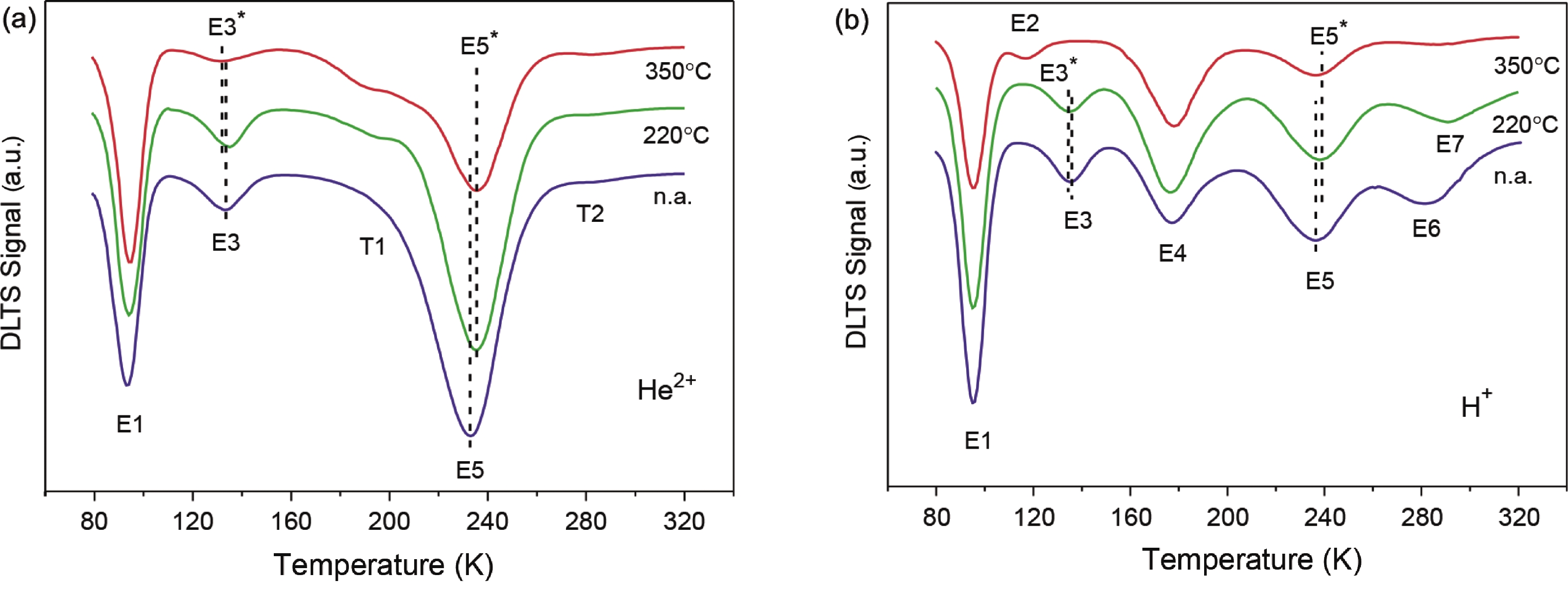
Table 2. Survey of deep level electron traps identified in proton and He irradiated silicon[69, 72].
| Level | Bandgap position (eV) | Capture cross section (cm2) | Identity |
| E1 | EC – 0.167 | σn = 4 × 10–15 | VO(–/0)+Ci–Cs (–/0) |
| E2 | EC – 0.213 | σn = 1 × 10–14 | ? (H-related) |
| E3 | EC – 0.252 | σn = 7 × 10–15 | V2=/– |
| E4 | EC – 0.312 | σn = 4 × 10–15 | VO–H |
| E5 | EC – 0.436 | σn = 3 × 10–15 | V2–/0 |
| E6 | EC – 0.463 | σn = 2 × 10–16 | H-related (V2H) |
| E7 | EC – 0.507 | σn = 6 × 10–17 | ? (H-related) |
 DownLoad: CSV
| [1] |
Mayer J, Marsh O. Ion implantation in semiconductors. Appl Solid State Sci, 1969, 1, 239 doi: 10.1016/S0065-2539(08)60539-9
|
| [2] |
Stephen J, Dearnaley G, Freeman J H, et al. Ion implantation. Book Review, 1973
|
| [3] |
Yuan Y, Xu C, Hübner R, et al. Interplay between localization and magnetism in (Ga, Mn)As and (In, Mn)As. Phys Rev Mater, 2017, 1, 054401 doi: 10.1103/PhysRevMaterials.1.054401
|
| [4] |
Yuan Y, Wang Y, Khalid M, et al. Ferromagnetic GaMnP prepared by ion implantation and pulsed laser annealing. IEEE Trans Mag, 2014, 50, 2401304 doi: 10.1109/TMAG.2014.2322332
|
| [5] |
Yuan Y, Wang M, Xu C, et al. Electronic phase separation in insulating (Ga, Mn)As with low compensation: Super-paramagnetism and hopping conduction. J Phys Condens Matter, 2018, 30, 095801 doi: 10.1088/1361-648X/aaa9a7
|
| [6] |
Yuan Y, Hübner R, Liu F, et al. Ferromagnetic Mn-implanted GaP: Microstructures vs magnetic properties. ACS Appl Mater & Interfaces, 2016, 8, 3912 doi: 10.1021/acsami.5b10949
|
| [7] |
Yuan Y, Wang Y, Gao K, et al. High Curie temperature and perpendicular magnetic anisotropy in homoepitaxial InMnAs films. J Phys D, 2015, 48, 235002 doi: 10.1088/0022-3727/48/23/235002
|
| [8] |
Prucnal S, Heera V, Hübner R, et al. Superconductivity in single-crystalline aluminum- and gallium-hyperdoped germanium. Phys Rev Mater, 2019, 3, 054802 doi: 10.1103/PhysRevMaterials.3.054802
|
| [9] |
Wang M, Berencén Y, García-Hemme E, et al. Extended infrared photoresponse in Te-hyperdoped Si at room temperature. Phys Rev Appl, 2018, 10, 024054 doi: 10.1103/PhysRevApplied.10.024054
|
| [10] |
Liu F, Prucnal S, Berencén Y, et al. Realizing the insulator-to-metal transition in Se-hyperdoped Si via non-equilibrium material processing. J Phys D, 2017, 50, 415102 doi: 10.1088/1361-6463/aa82f9
|
| [11] |
Ziegler J F, Ziegler M D, Biersack J B. SRIM-The stopping and range of ions in matter (2010). Nucl Instrum Methods Phys Res Sect B, 2010, 268, 1818 doi: 10.1016/j.nimb.2010.02.091
|
| [12] |
Zhou S, Chen X L. Defect-induced magnetism in SiC. J Phys D, 2019, 52, 393001 doi: 10.1088/1361-6463/ab2495
|
| [13] |
Lee P A, Ramakrishnan T V. Disordered electronic systems. Rev Mod Phys, 1985, 57, 287 doi: 10.1103/RevModPhys.57.287
|
| [14] |
Pantelides S T. The electronic structure of impurities and other point defects in semiconductors. Rev Mod Phys, 1978, 50, 797 doi: 10.1103/RevModPhys.50.797
|
| [15] |
Park J, Choi J H, Kong K, et al. Electrically driven mid-submicrometre pixelation of InGaN micro-light-emitting diode displays for augmented-reality glasses. Nat Photonics, 2021, 15, 449 doi: 10.1038/s41566-021-00783-1
|
| [16] |
Zhou S, Li L, Yuan Y, et al. Precise tuning of the Curie temperature of (Ga, Mn)As-based magnetic semiconductors by hole compensation: Support for valence-band ferromagnetism. Phy Rev B, 2016, 94, 075205 doi: 10.1103/PhysRevB.94.075205
|
| [17] |
Xu C, Wang M, Yuan Y, et al. Hole compensation effect in III-Mn-V dilute ferromagnetic semiconductors. J Phys D, 2019, 52, 355301 doi: 10.1088/1361-6463/ab25dd
|
| [18] |
Rischau C W, Leridon B, Fauqué B, et al. Doping of Bi2Te3 using electron irradiation. Phys Rev B, 2013, 88, 205207 doi: 10.1103/PhysRevB.88.205207
|
| [19] |
Liu Y, Li Z, Guo L, et al. Towards diluted magnetism in TaAs. Phys Rev Mater, 2017, 1, 044203 doi: 10.1103/PhysRevMaterials.1.044203
|
| [20] |
Hazdra P, Popelka S, Schöner A. Optimization of SiC power p-i-n diode parameters by proton irradiation. IEEE Trans Electron Devices, 2018, 65, 4483 doi: 10.1109/TED.2018.2866763
|
| [21] |
Sharma R K, Hazdra P, Popelka S. The effect of light ion irradiation on 4H-SiC MPS power diode characteristics: Experiment and simulation. IEEE Trans Nucl Sci, 2015, 62, 534 doi: 10.1109/TNS.2015.2395712
|
| [22] |
Aspar B, Bruel M, Moriceau H, et al. Basic mechanisms involved in the Smart-Cut® process. Microelectron J, 1997, 36, 233 doi: 10.1016/S0167-9317(97)00055-5
|
| [23] |
Bruel M, Aspar B, Auberton-Hervé A J. Smart-Cut: A new silicon on insulator material technology based on hydrogen implantation and wafer bonding. J Jpn Appl Phys, 1997, 36, 1636 doi: 10.1143/JJAP.36.1636
|
| [24] |
Dietl T, Ohno H, Matsukura F, et al. Zener model description of ferromagnetism in zinc-blende magnetic semiconductors. Science, 2000, 287, 1019 doi: 10.1126/science.287.5455
|
| [25] |
Y Yuan, T Amarouche, C Xu, et al. Switching the uniaxial magnetic anisotropy by ion irradiation induced compensation. J Phys D, 2018, 51, 145001 doi: 10.1088/1361-6463/aab1db
|
| [26] |
Dobrowolska M, Tivakornsasithorn K, Liu X, et al. Controlling the Curie temperature in (Ga, Mn)As through location of the Fermi level within the impurity band. Nat Mater, 2012, 11, 444 doi: 10.1038/nmat3250
|
| [27] |
Goennenwein S T B, Wassner T A, Huebl H, et al. Hydrogen control of ferromagnetism in a dilute magnetic semiconductor. Phys Rev Lett, 2004, 92, 227202 doi: 10.1103/PhysRevLett.92.227202
|
| [28] |
Sinnecker E H C P, Penello G M, Rappoport T G, et al. Ion-beam modification of the magnetic properties of Ga1− xMn xAs epilayers. Phys Rev B, 2010, 81, 245203 doi: 10.1103/PhysRevB.81.245203
|
| [29] |
Kudrawiec R. Conduction and valence band positions versus the Fermi-level stabilization energy in quaternary dilute nitrides. Phys Status Solidi C, 2011, 8, 1650 doi: 10.1002/pssc.201000833
|
| [30] |
Wang C, Chang C H, Huang A, et al. Tunable disorder and localization in the rare-earth nickelates. Phys Rev Mater, 2019, 3, 053801 doi: 10.1103/PhysRevMaterials.3.053801
|
| [31] |
Evers F, Mirlin A D. Anderson transitions. Rev Mod Phys, 2008, 80, 1355 doi: 10.1103/RevModPhys.80.1355
|
| [32] |
Smylie M P, Claus H, Kwok W K, et al. Superconductivity, pairing symmetry, and disorder in the doped topological insulator Sn1− xIn xTe for x > 0.10. Phys Rev B, 2018, 97, 024511 doi: 10.1103/PhysRevB.97.024511
|
| [33] |
Harimohan V, Bharathi A, Rajaraman R, et al. Magneto-resistance in pristine and irradiated TaAs2. AIP Adv, 2019, 9, 045020 doi: 10.1063/1.5087772
|
| [34] |
Shoenberg D. Magnetic oscillations in metals. Cambridge University Press, Cambridge, 1984
|
| [35] |
Hashibon A, Elsässer C. First-principles density functional theory study of native point defects in Bi2Te3. Phys Rev B, 2011, 84, 144117 doi: 10.1103/PhysRevB.84.144117
|
| [36] |
Pecheur P, Toussaint G. Tight-binding studies of crystal stability and defects in Bi2Te3. J Phys Chem Solids, 1994, 55, 327 doi: 10.1016/0022-3697(94)90229-1
|
| [37] |
Chaudhari P, Bever M B. Effects of irradiation with protons on the electrical properties of Bi2Te3. J Appl Phys, 1966, 37, 4181 doi: 10.1063/1.1707997
|
| [38] |
Chaudhari P, Bever M B. Defects in the compound Bi2Te3 caused by irradiation with protons. J Appl Phys, 1967, 38, 2417 doi: 10.1063/1.1709917
|
| [39] |
Smylie M P, Willa K, Claus H, et al. Robust odd-parity superconductivity in the doped topological insulator Nb xBi2Se3. Phys Rev B, 2017, 96, 115145 doi: 10.1103/PhysRevB.96.115145
|
| [40] |
Kimoto T, Cooper J A. Fundamentals of silicon carbide technology. Singapore: Wiley, 2014
|
| [41] |
Vobecký J, Hazdra P, Záhlava V, et al. ON-state characteristics of proton irradiated 4H–SiC Schottky diode: The calibration of model parameters for device simulation. Solid-State Electron, 2014, 94, 32 doi: 10.1016/j.sse.2014.02.004
|
| [42] |
Vobecký J, Hazdra P, Sharma S, et al. Impact of electron irradiation on the On-state characteristics of a 4H-SiC JBS diode. IEEE Trans Electron Devices, 2015, 62, 1964 doi: 10.1109/TED.2015.2421503
|
| [43] |
Hiyoshi T, Kimoto T. Reduction of deep levels and improvement of carrier lifetime in n-type 4H-SiC by thermal oxidation. Appl Phys Express, 2009, 2, 041101 doi: 10.1143/APEX.2.041101
|
| [44] |
Hazdra P, Popelka S, Záhlava V, et al. Radiation damage in 4H-SiC and its effect on power device characteristics. Solid State Phenomena, 2015, 242, 421 doi: 10.4028/www.scientific.net/SSP.242.421
|
| [45] |
Williams J S. Ion implantation of semiconductors. Mater Sci Eng A, 1998, 253, 8 doi: 10.1016/S0921-5093(98)00705-9
|
| [46] |
Hallén A, M S Janson, YuKuznetsov A, et al. Ion implantation of silicon carbide. Nucl Instrum Methods Phys Res Sect B, 2002, 186, 186 doi: 10.1016/S0168-583X(01)00880-1
|
| [47] |
Zolper J C. Ion implantation in group III-nitride semiconductors: a tool for doping and defect studies. J Crys Growth, 1997, 178, 157 doi: 10.1016/S0022-0248(97)00076-6
|
| [48] |
Pearton S J. Ion implantation in III–V semiconductor technology. Int J Mod Phys B, 1993, 7, 4687 doi: 10.1142/S0217979293003814
|
| [49] |
Alfieri G, Monakhov E V, Svensson B G, et al. Annealing behavior between room temperature and 2000 °C of deep level defects in electron-irradiated n-type 4H silicon carbide. J Appl Phys, 2005, 98, 043518 doi: 10.1063/1.2009816
|
| [50] |
Zippelius B, Suda J, Kimoto T. High temperature annealing of n-type 4H-SiC: Impact on intrinsic defects and carrier lifetime. J Appl Phys, 2012, 111, 033515 doi: 10.1063/1.3681806
|
| [51] |
Dalibor T, Pensl G, Matsunami H, et al. Deep defect centers in silicon carbide monitored with deep level transient spectroscopy. Phys Status Solidi A, 1997, 162, 199 doi: 10.1002/1521-396X(199707)162:1<199::AID-PSSA199>3.0.CO;2-0
|
| [52] |
Klein P B, Shanabrook B V, Huh S W, et al. Lifetime-limiting defects in n- 4H-SiC epilayers. Appl Phys Lett, 2006, 88, 052110 doi: 10.1063/1.2170144
|
| [53] |
Pintilie I, Pintilie L, Irmscher K, et al. Formation of the Z1,2 deep-level defects in 4H-SiC epitaxial layers: Evidence for nitrogen participation. Appl Phys Lett, 2002, 81, 4841 doi: 10.1063/1.1529314
|
| [54] |
Eberlein T A G, Jones R, Briddon P R. Z1/Z2 defects in 4H-SiC. Phys Rev Lett, 2003, 90, 225502 doi: 10.1103/PhysRevLett.90.225502
|
| [55] |
Storasta L, Henry A, Bergman J P, et al. Investigations of possible nitrogen participation in the Z1/Z2 defect in 4H-SiC. Mater Sci Forum, 2004, 457–460, 469 doi: 10.4028/www.scientific.net/MSF.457-460.469
|
| [56] |
Storasta L, Tsuchida H. Reduction of traps and improvement of carrier lifetime in epilayers by ion implantation. Appl Phys Lett, 2007, 90, 062116 doi: 10.1063/1.2472530
|
| [57] |
Storasta L, Tsuchida H, Miyazawa T. Enhanced annealing of the Z1/2 defect in 4H–SiC epilayers. J Appl Phys, 2008, 103, 013705 doi: 10.1063/1.2829776
|
| [58] |
Ichikawa S, Kawahara K, Suda J, et al. Carrier recombination in n-type 4H-SiC epilayers with long carrier lifetimes. Appl Phys Express, 2012, 5, 101301 doi: 10.1143/APEX.5.101301
|
| [59] |
Hazdra P, Popelka S, Schöner A. Local lifetime control in 4H-SiC by proton irradiation. Mater Sci Forum, 2018, 924, 436 doi: 10.4028/www.scientific.net/MSF.924.436
|
| [60] |
Achtziger N, Pasold G, Sielemann R, et al. Tungsten in silicon carbide: Band-gap states and their polytype dependence. Phys Rev B, 2000, 62, 12888 doi: 10.1103/PhysRevB.62.12888
|
| [61] |
Hemmingsson C, Son N T, Kordina O, et al. Deep level defects in electron-irradiated 4H SiC epitaxial layers. J Appl Phys, 1997, 81, 6155 doi: 10.1063/1.364397
|
| [62] |
Storasta L, Bergman J P, Janzén E, et al. Deep levels created by low energy electron irradiation in 4H-SiC. J Appl Phys, 2004, 96, 4909 doi: 10.1063/1.1778819
|
| [63] |
Hazdra P, Popelka S. Lifetime control in SiC PiN diodes using radiation defects. Mater Sci Forum, 2017, 897, 463 doi: 10.4028/www.scientific.net/MSF.897.463
|
| [64] |
Son N T, Trinh X T, Løvlie L S, et al. Negative-U system of carbon vacancy in 4H-SiC. Phys Rev Lett, 2012, 109, 187603 doi: 10.1103/PhysRevLett.109.187603
|
| [65] |
Vobecký J, Hazdra P, Záhlava V. Open circuit voltage decay lifetime of ion irradiated devices. Microelectron J, 1999, 30, 513 doi: 10.1016/S0026-2692(98)00173-6
|
| [66] |
Guerriero P, Sanseverino A, Daliento S. Lifetime profile reconstruction in helium implanted silicon for planar IGBTs. 29th International Conference on Microelectronics Proceedings - MIEL 2014, Belgrade, 2014, 325
|
| [67] |
Hazdra P, Brand K, Rubeš J, et al. Local lifetime control by light ion irradiation: impact on blocking capability of power P–i–N diode. Microelectron J, 2001, 32, 449 doi: 10.1016/S0026-2692(01)00014-3
|
| [68] |
Napoli E, Strollo A G M, Spirito P. Numerical analysis of local lifetime control for high-speed low-loss P-i-N diode design. IEEE Trans Power Electron, 1999, 14, 615 doi: 10.1109/63.774197
|
| [69] |
Hazdra P, Komarnitskyy V. Lifetime control in silicon power P-i-N diode by ion irradiation: Suppression of undesired leakage. Microelectron J, 2006, 37, 197 doi: 10.1016/j.mejo.2005.09.010
|
| [70] |
Kohno I. Production of fast-switching power thyristors by proton irradiation. Nucl Instrum Methods Phys Res Sect B, 1989, 37/38, 739 doi: 10.1016/0168-583X(89)90288-7
|
| [71] |
Sawko D C, Bartko J. Production of fast switching power thyristors by proton irradiation. IEEE Trans Nucl Sci, 1983, 30, 1756 doi: 10.1109/TNS.1983.4332634
|
| [72] |
Hazdra P, Brand K, Vobecky J. Effect of defects produced by MeV H and He ion implantation on characteristic of power silicon P-i-N diodes. 2000 International Conference on Ion Implantation Technology, 2000, 135
|
| [73] |
Hazdra P, Vobecky J, Dorschner H, et al. Axial lifetime control in silicon power diodes by irradiation with protons, alphas, low- and high-energy electrons. Microelectron J, 2004, 35, 249 doi: 10.1016/S0026-2692(03)00194-0
|
| [74] |
Hazdra P, Rubeš J, Vobecký J. Divacancy profiles in MeV helium irradiated silicon from reverse I–V measurement. Nucl Instrum Methods Phys Res Sect B, 1999, 159, 207 doi: 10.1016/S0168-583X(99)00565-0
|
| [75] |
Vobecky J, Hazdra P, Zahlava V. Helium irradiated high-power P-i-N diode with low On-state voltage drop. Solid-State Electron, 2003, 47, 45 doi: 10.1016/S0038-1101(02)00250-2
|
| [76] |
Vobecky J, Hazdra P. The application of platinum-silicide anode layer to decrease the static and turn-off losses in high-power P-i-N diode. Thin Solid Films, 2003, 433, 305 doi: 10.1016/S0040-6090(03)00299-2
|
| [77] |
Vobecky J, Hazdra P. Advanced local lifetime control for higher reliability of power devices. Microelectron Reliab, 2003, 42, 1883 doi: 10.1016/S0026-2714(03)00320-2
|
| [78] |
Prabhakar A, McGill T C, Nicolet M A. Platinum diffusion into silicon from PtSi. Appl Phys Lett, 1983, 43, 1118 doi: 10.1063/1.94247
|
| [79] |
Schmidt D C, Svensson G, Godey S, et al. The influence of diffusion temperature and ion dose on proximity gettering of platinum in silicon implanted with alpha particles at low doses. Appl Phys Lett, 1999, 74, 3329 doi: 10.1063/1.123334
|
| [80] |
Seol D, Kim S, Jang W S, et al. Selective patterning of out-of-plane piezoelectricity in MoTe2 via focused ion beam. Nano Energy, 2021, 79, 105451 doi: 10.1016/j.nanoen.2020.105451
|
| [81] |
Mitterreiter E, Schuler B, Cochrane K A, et al. Atomistic positioning of defects in helium ion treated single-layer MoS2. Nano Lett, 2020, 20, 4437 doi: 10.1021/acs.nanolett.0c01222
|
| [82] |
Babin C, Stöhr R, Morioka N, et al. Fabrication and nanophotonic waveguide integration of silicon carbide colour centres with preserved spin-optical coherence. Nat Mater, 2022, 21, 67 doi: 10.1038/s41563-021-01148-3
|
| [83] |
Kasper C, Klenkert D, Shang Z, et al. Influence of irradiation on defect spin coherence in silicon carbide. Phys Rev Appl, 2020, 13, 044054 doi: 10.1103/PhysRevApplied.13.044054
|
| [84] |
Bathen M E, Vines L. Manipulating single-photon emission from point defects in diamond and silicon carbide. Adv Quantum Technol, 2021, 4, 2100003 doi: 10.1002/qute.202100003
|
| [85] |
Xiong W, Zhou X, Xu G, et al. Double-barrier-Ga2O3 Schottky barrier diode with low turn-on voltage and leakage current. IEEE Electron Device Lett, 2021, 42, 430 doi: 10.1109/LED.2021.3055349
|
| [86] |
He Q, Hao W, Zhou X, et al. Over 1 GW/cm2 vertical Ga2O3 Schottky barrier diodes without edge termination. IEEE Electron Device Lett, 2022, 43, 264 doi: 10.1109/LED.2021.3133866
|
| [87] |
Hao W, He Q, Zhou K, et al. Low defect density and small curve hysteresis in NiO/β-Ga2O3 pn diode with a high PFOM of 0.65 GW/cm2. Appl Phys Lett, 2021, 118, 043501 doi: 10.1063/5.0038349
|
| [88] |
Hou X, Zhao X, Zhang Y, et al. High-performance harsh-environment-resistant GaOx solar-blind photodetectors via defect and doping engineering. Adv Mater, 2022, 34, 2106923 doi: 10.1002/adma.202106923
|


Article views: 961 Times PDF downloads: 79 Times Cited by: 0 Times
Received: 17 November 2021 Revised: 05 March 2022 Online: Accepted Manuscript: 10 May 2022Uncorrected proof: 12 May 2022Published: 06 June 2022
| Citation: |
Ye Yuan, Shengqiang Zhou, Xinqiang Wang. Modulating properties by light ion irradiation: From novel functional materials to semiconductor power devices[J]. Journal of Semiconductors, 2022, 43(6): 063101. doi: 10.1088/1674-4926/43/6/063101
Y Yuan, S Q Zhou, X Q Wang. Modulating properties by light ion irradiation: From novel functional materials to semiconductor power devices[J]. J. Semicond, 2022, 43(6): 063101. doi: 10.1088/1674-4926/43/6/063101
Export: BibTex EndNote

|
| [1] |
Mayer J, Marsh O. Ion implantation in semiconductors. Appl Solid State Sci, 1969, 1, 239 doi: 10.1016/S0065-2539(08)60539-9
|
| [2] |
Stephen J, Dearnaley G, Freeman J H, et al. Ion implantation. Book Review, 1973
|
| [3] |
Yuan Y, Xu C, Hübner R, et al. Interplay between localization and magnetism in (Ga, Mn)As and (In, Mn)As. Phys Rev Mater, 2017, 1, 054401 doi: 10.1103/PhysRevMaterials.1.054401
|
| [4] |
Yuan Y, Wang Y, Khalid M, et al. Ferromagnetic GaMnP prepared by ion implantation and pulsed laser annealing. IEEE Trans Mag, 2014, 50, 2401304 doi: 10.1109/TMAG.2014.2322332
|
| [5] |
Yuan Y, Wang M, Xu C, et al. Electronic phase separation in insulating (Ga, Mn)As with low compensation: Super-paramagnetism and hopping conduction. J Phys Condens Matter, 2018, 30, 095801 doi: 10.1088/1361-648X/aaa9a7
|
| [6] |
Yuan Y, Hübner R, Liu F, et al. Ferromagnetic Mn-implanted GaP: Microstructures vs magnetic properties. ACS Appl Mater & Interfaces, 2016, 8, 3912 doi: 10.1021/acsami.5b10949
|
| [7] |
Yuan Y, Wang Y, Gao K, et al. High Curie temperature and perpendicular magnetic anisotropy in homoepitaxial InMnAs films. J Phys D, 2015, 48, 235002 doi: 10.1088/0022-3727/48/23/235002
|
| [8] |
Prucnal S, Heera V, Hübner R, et al. Superconductivity in single-crystalline aluminum- and gallium-hyperdoped germanium. Phys Rev Mater, 2019, 3, 054802 doi: 10.1103/PhysRevMaterials.3.054802
|
| [9] |
Wang M, Berencén Y, García-Hemme E, et al. Extended infrared photoresponse in Te-hyperdoped Si at room temperature. Phys Rev Appl, 2018, 10, 024054 doi: 10.1103/PhysRevApplied.10.024054
|
| [10] |
Liu F, Prucnal S, Berencén Y, et al. Realizing the insulator-to-metal transition in Se-hyperdoped Si via non-equilibrium material processing. J Phys D, 2017, 50, 415102 doi: 10.1088/1361-6463/aa82f9
|
| [11] |
Ziegler J F, Ziegler M D, Biersack J B. SRIM-The stopping and range of ions in matter (2010). Nucl Instrum Methods Phys Res Sect B, 2010, 268, 1818 doi: 10.1016/j.nimb.2010.02.091
|
| [12] |
Zhou S, Chen X L. Defect-induced magnetism in SiC. J Phys D, 2019, 52, 393001 doi: 10.1088/1361-6463/ab2495
|
| [13] |
Lee P A, Ramakrishnan T V. Disordered electronic systems. Rev Mod Phys, 1985, 57, 287 doi: 10.1103/RevModPhys.57.287
|
| [14] |
Pantelides S T. The electronic structure of impurities and other point defects in semiconductors. Rev Mod Phys, 1978, 50, 797 doi: 10.1103/RevModPhys.50.797
|
| [15] |
Park J, Choi J H, Kong K, et al. Electrically driven mid-submicrometre pixelation of InGaN micro-light-emitting diode displays for augmented-reality glasses. Nat Photonics, 2021, 15, 449 doi: 10.1038/s41566-021-00783-1
|
| [16] |
Zhou S, Li L, Yuan Y, et al. Precise tuning of the Curie temperature of (Ga, Mn)As-based magnetic semiconductors by hole compensation: Support for valence-band ferromagnetism. Phy Rev B, 2016, 94, 075205 doi: 10.1103/PhysRevB.94.075205
|
| [17] |
Xu C, Wang M, Yuan Y, et al. Hole compensation effect in III-Mn-V dilute ferromagnetic semiconductors. J Phys D, 2019, 52, 355301 doi: 10.1088/1361-6463/ab25dd
|
| [18] |
Rischau C W, Leridon B, Fauqué B, et al. Doping of Bi2Te3 using electron irradiation. Phys Rev B, 2013, 88, 205207 doi: 10.1103/PhysRevB.88.205207
|
| [19] |
Liu Y, Li Z, Guo L, et al. Towards diluted magnetism in TaAs. Phys Rev Mater, 2017, 1, 044203 doi: 10.1103/PhysRevMaterials.1.044203
|
| [20] |
Hazdra P, Popelka S, Schöner A. Optimization of SiC power p-i-n diode parameters by proton irradiation. IEEE Trans Electron Devices, 2018, 65, 4483 doi: 10.1109/TED.2018.2866763
|
| [21] |
Sharma R K, Hazdra P, Popelka S. The effect of light ion irradiation on 4H-SiC MPS power diode characteristics: Experiment and simulation. IEEE Trans Nucl Sci, 2015, 62, 534 doi: 10.1109/TNS.2015.2395712
|
| [22] |
Aspar B, Bruel M, Moriceau H, et al. Basic mechanisms involved in the Smart-Cut® process. Microelectron J, 1997, 36, 233 doi: 10.1016/S0167-9317(97)00055-5
|
| [23] |
Bruel M, Aspar B, Auberton-Hervé A J. Smart-Cut: A new silicon on insulator material technology based on hydrogen implantation and wafer bonding. J Jpn Appl Phys, 1997, 36, 1636 doi: 10.1143/JJAP.36.1636
|
| [24] |
Dietl T, Ohno H, Matsukura F, et al. Zener model description of ferromagnetism in zinc-blende magnetic semiconductors. Science, 2000, 287, 1019 doi: 10.1126/science.287.5455
|
| [25] |
Y Yuan, T Amarouche, C Xu, et al. Switching the uniaxial magnetic anisotropy by ion irradiation induced compensation. J Phys D, 2018, 51, 145001 doi: 10.1088/1361-6463/aab1db
|
| [26] |
Dobrowolska M, Tivakornsasithorn K, Liu X, et al. Controlling the Curie temperature in (Ga, Mn)As through location of the Fermi level within the impurity band. Nat Mater, 2012, 11, 444 doi: 10.1038/nmat3250
|
| [27] |
Goennenwein S T B, Wassner T A, Huebl H, et al. Hydrogen control of ferromagnetism in a dilute magnetic semiconductor. Phys Rev Lett, 2004, 92, 227202 doi: 10.1103/PhysRevLett.92.227202
|
| [28] |
Sinnecker E H C P, Penello G M, Rappoport T G, et al. Ion-beam modification of the magnetic properties of Ga1− xMn xAs epilayers. Phys Rev B, 2010, 81, 245203 doi: 10.1103/PhysRevB.81.245203
|
| [29] |
Kudrawiec R. Conduction and valence band positions versus the Fermi-level stabilization energy in quaternary dilute nitrides. Phys Status Solidi C, 2011, 8, 1650 doi: 10.1002/pssc.201000833
|
| [30] |
Wang C, Chang C H, Huang A, et al. Tunable disorder and localization in the rare-earth nickelates. Phys Rev Mater, 2019, 3, 053801 doi: 10.1103/PhysRevMaterials.3.053801
|
| [31] |
Evers F, Mirlin A D. Anderson transitions. Rev Mod Phys, 2008, 80, 1355 doi: 10.1103/RevModPhys.80.1355
|
| [32] |
Smylie M P, Claus H, Kwok W K, et al. Superconductivity, pairing symmetry, and disorder in the doped topological insulator Sn1− xIn xTe for x > 0.10. Phys Rev B, 2018, 97, 024511 doi: 10.1103/PhysRevB.97.024511
|
| [33] |
Harimohan V, Bharathi A, Rajaraman R, et al. Magneto-resistance in pristine and irradiated TaAs2. AIP Adv, 2019, 9, 045020 doi: 10.1063/1.5087772
|
| [34] |
Shoenberg D. Magnetic oscillations in metals. Cambridge University Press, Cambridge, 1984
|
| [35] |
Hashibon A, Elsässer C. First-principles density functional theory study of native point defects in Bi2Te3. Phys Rev B, 2011, 84, 144117 doi: 10.1103/PhysRevB.84.144117
|
| [36] |
Pecheur P, Toussaint G. Tight-binding studies of crystal stability and defects in Bi2Te3. J Phys Chem Solids, 1994, 55, 327 doi: 10.1016/0022-3697(94)90229-1
|
| [37] |
Chaudhari P, Bever M B. Effects of irradiation with protons on the electrical properties of Bi2Te3. J Appl Phys, 1966, 37, 4181 doi: 10.1063/1.1707997
|
| [38] |
Chaudhari P, Bever M B. Defects in the compound Bi2Te3 caused by irradiation with protons. J Appl Phys, 1967, 38, 2417 doi: 10.1063/1.1709917
|
| [39] |
Smylie M P, Willa K, Claus H, et al. Robust odd-parity superconductivity in the doped topological insulator Nb xBi2Se3. Phys Rev B, 2017, 96, 115145 doi: 10.1103/PhysRevB.96.115145
|
| [40] |
Kimoto T, Cooper J A. Fundamentals of silicon carbide technology. Singapore: Wiley, 2014
|
| [41] |
Vobecký J, Hazdra P, Záhlava V, et al. ON-state characteristics of proton irradiated 4H–SiC Schottky diode: The calibration of model parameters for device simulation. Solid-State Electron, 2014, 94, 32 doi: 10.1016/j.sse.2014.02.004
|
| [42] |
Vobecký J, Hazdra P, Sharma S, et al. Impact of electron irradiation on the On-state characteristics of a 4H-SiC JBS diode. IEEE Trans Electron Devices, 2015, 62, 1964 doi: 10.1109/TED.2015.2421503
|
| [43] |
Hiyoshi T, Kimoto T. Reduction of deep levels and improvement of carrier lifetime in n-type 4H-SiC by thermal oxidation. Appl Phys Express, 2009, 2, 041101 doi: 10.1143/APEX.2.041101
|
| [44] |
Hazdra P, Popelka S, Záhlava V, et al. Radiation damage in 4H-SiC and its effect on power device characteristics. Solid State Phenomena, 2015, 242, 421 doi: 10.4028/www.scientific.net/SSP.242.421
|
| [45] |
Williams J S. Ion implantation of semiconductors. Mater Sci Eng A, 1998, 253, 8 doi: 10.1016/S0921-5093(98)00705-9
|
| [46] |
Hallén A, M S Janson, YuKuznetsov A, et al. Ion implantation of silicon carbide. Nucl Instrum Methods Phys Res Sect B, 2002, 186, 186 doi: 10.1016/S0168-583X(01)00880-1
|
| [47] |
Zolper J C. Ion implantation in group III-nitride semiconductors: a tool for doping and defect studies. J Crys Growth, 1997, 178, 157 doi: 10.1016/S0022-0248(97)00076-6
|
| [48] |
Pearton S J. Ion implantation in III–V semiconductor technology. Int J Mod Phys B, 1993, 7, 4687 doi: 10.1142/S0217979293003814
|
| [49] |
Alfieri G, Monakhov E V, Svensson B G, et al. Annealing behavior between room temperature and 2000 °C of deep level defects in electron-irradiated n-type 4H silicon carbide. J Appl Phys, 2005, 98, 043518 doi: 10.1063/1.2009816
|
| [50] |
Zippelius B, Suda J, Kimoto T. High temperature annealing of n-type 4H-SiC: Impact on intrinsic defects and carrier lifetime. J Appl Phys, 2012, 111, 033515 doi: 10.1063/1.3681806
|
| [51] |
Dalibor T, Pensl G, Matsunami H, et al. Deep defect centers in silicon carbide monitored with deep level transient spectroscopy. Phys Status Solidi A, 1997, 162, 199 doi: 10.1002/1521-396X(199707)162:1<199::AID-PSSA199>3.0.CO;2-0
|
| [52] |
Klein P B, Shanabrook B V, Huh S W, et al. Lifetime-limiting defects in n- 4H-SiC epilayers. Appl Phys Lett, 2006, 88, 052110 doi: 10.1063/1.2170144
|
| [53] |
Pintilie I, Pintilie L, Irmscher K, et al. Formation of the Z1,2 deep-level defects in 4H-SiC epitaxial layers: Evidence for nitrogen participation. Appl Phys Lett, 2002, 81, 4841 doi: 10.1063/1.1529314
|
| [54] |
Eberlein T A G, Jones R, Briddon P R. Z1/Z2 defects in 4H-SiC. Phys Rev Lett, 2003, 90, 225502 doi: 10.1103/PhysRevLett.90.225502
|
| [55] |
Storasta L, Henry A, Bergman J P, et al. Investigations of possible nitrogen participation in the Z1/Z2 defect in 4H-SiC. Mater Sci Forum, 2004, 457–460, 469 doi: 10.4028/www.scientific.net/MSF.457-460.469
|
| [56] |
Storasta L, Tsuchida H. Reduction of traps and improvement of carrier lifetime in epilayers by ion implantation. Appl Phys Lett, 2007, 90, 062116 doi: 10.1063/1.2472530
|
| [57] |
Storasta L, Tsuchida H, Miyazawa T. Enhanced annealing of the Z1/2 defect in 4H–SiC epilayers. J Appl Phys, 2008, 103, 013705 doi: 10.1063/1.2829776
|
| [58] |
Ichikawa S, Kawahara K, Suda J, et al. Carrier recombination in n-type 4H-SiC epilayers with long carrier lifetimes. Appl Phys Express, 2012, 5, 101301 doi: 10.1143/APEX.5.101301
|
| [59] |
Hazdra P, Popelka S, Schöner A. Local lifetime control in 4H-SiC by proton irradiation. Mater Sci Forum, 2018, 924, 436 doi: 10.4028/www.scientific.net/MSF.924.436
|
| [60] |
Achtziger N, Pasold G, Sielemann R, et al. Tungsten in silicon carbide: Band-gap states and their polytype dependence. Phys Rev B, 2000, 62, 12888 doi: 10.1103/PhysRevB.62.12888
|
| [61] |
Hemmingsson C, Son N T, Kordina O, et al. Deep level defects in electron-irradiated 4H SiC epitaxial layers. J Appl Phys, 1997, 81, 6155 doi: 10.1063/1.364397
|
| [62] |
Storasta L, Bergman J P, Janzén E, et al. Deep levels created by low energy electron irradiation in 4H-SiC. J Appl Phys, 2004, 96, 4909 doi: 10.1063/1.1778819
|
| [63] |
Hazdra P, Popelka S. Lifetime control in SiC PiN diodes using radiation defects. Mater Sci Forum, 2017, 897, 463 doi: 10.4028/www.scientific.net/MSF.897.463
|
| [64] |
Son N T, Trinh X T, Løvlie L S, et al. Negative-U system of carbon vacancy in 4H-SiC. Phys Rev Lett, 2012, 109, 187603 doi: 10.1103/PhysRevLett.109.187603
|
| [65] |
Vobecký J, Hazdra P, Záhlava V. Open circuit voltage decay lifetime of ion irradiated devices. Microelectron J, 1999, 30, 513 doi: 10.1016/S0026-2692(98)00173-6
|
| [66] |
Guerriero P, Sanseverino A, Daliento S. Lifetime profile reconstruction in helium implanted silicon for planar IGBTs. 29th International Conference on Microelectronics Proceedings - MIEL 2014, Belgrade, 2014, 325
|
| [67] |
Hazdra P, Brand K, Rubeš J, et al. Local lifetime control by light ion irradiation: impact on blocking capability of power P–i–N diode. Microelectron J, 2001, 32, 449 doi: 10.1016/S0026-2692(01)00014-3
|
| [68] |
Napoli E, Strollo A G M, Spirito P. Numerical analysis of local lifetime control for high-speed low-loss P-i-N diode design. IEEE Trans Power Electron, 1999, 14, 615 doi: 10.1109/63.774197
|
| [69] |
Hazdra P, Komarnitskyy V. Lifetime control in silicon power P-i-N diode by ion irradiation: Suppression of undesired leakage. Microelectron J, 2006, 37, 197 doi: 10.1016/j.mejo.2005.09.010
|
| [70] |
Kohno I. Production of fast-switching power thyristors by proton irradiation. Nucl Instrum Methods Phys Res Sect B, 1989, 37/38, 739 doi: 10.1016/0168-583X(89)90288-7
|
| [71] |
Sawko D C, Bartko J. Production of fast switching power thyristors by proton irradiation. IEEE Trans Nucl Sci, 1983, 30, 1756 doi: 10.1109/TNS.1983.4332634
|
| [72] |
Hazdra P, Brand K, Vobecky J. Effect of defects produced by MeV H and He ion implantation on characteristic of power silicon P-i-N diodes. 2000 International Conference on Ion Implantation Technology, 2000, 135
|
| [73] |
Hazdra P, Vobecky J, Dorschner H, et al. Axial lifetime control in silicon power diodes by irradiation with protons, alphas, low- and high-energy electrons. Microelectron J, 2004, 35, 249 doi: 10.1016/S0026-2692(03)00194-0
|
| [74] |
Hazdra P, Rubeš J, Vobecký J. Divacancy profiles in MeV helium irradiated silicon from reverse I–V measurement. Nucl Instrum Methods Phys Res Sect B, 1999, 159, 207 doi: 10.1016/S0168-583X(99)00565-0
|
| [75] |
Vobecky J, Hazdra P, Zahlava V. Helium irradiated high-power P-i-N diode with low On-state voltage drop. Solid-State Electron, 2003, 47, 45 doi: 10.1016/S0038-1101(02)00250-2
|
| [76] |
Vobecky J, Hazdra P. The application of platinum-silicide anode layer to decrease the static and turn-off losses in high-power P-i-N diode. Thin Solid Films, 2003, 433, 305 doi: 10.1016/S0040-6090(03)00299-2
|
| [77] |
Vobecky J, Hazdra P. Advanced local lifetime control for higher reliability of power devices. Microelectron Reliab, 2003, 42, 1883 doi: 10.1016/S0026-2714(03)00320-2
|
| [78] |
Prabhakar A, McGill T C, Nicolet M A. Platinum diffusion into silicon from PtSi. Appl Phys Lett, 1983, 43, 1118 doi: 10.1063/1.94247
|
| [79] |
Schmidt D C, Svensson G, Godey S, et al. The influence of diffusion temperature and ion dose on proximity gettering of platinum in silicon implanted with alpha particles at low doses. Appl Phys Lett, 1999, 74, 3329 doi: 10.1063/1.123334
|
| [80] |
Seol D, Kim S, Jang W S, et al. Selective patterning of out-of-plane piezoelectricity in MoTe2 via focused ion beam. Nano Energy, 2021, 79, 105451 doi: 10.1016/j.nanoen.2020.105451
|
| [81] |
Mitterreiter E, Schuler B, Cochrane K A, et al. Atomistic positioning of defects in helium ion treated single-layer MoS2. Nano Lett, 2020, 20, 4437 doi: 10.1021/acs.nanolett.0c01222
|
| [82] |
Babin C, Stöhr R, Morioka N, et al. Fabrication and nanophotonic waveguide integration of silicon carbide colour centres with preserved spin-optical coherence. Nat Mater, 2022, 21, 67 doi: 10.1038/s41563-021-01148-3
|
| [83] |
Kasper C, Klenkert D, Shang Z, et al. Influence of irradiation on defect spin coherence in silicon carbide. Phys Rev Appl, 2020, 13, 044054 doi: 10.1103/PhysRevApplied.13.044054
|
| [84] |
Bathen M E, Vines L. Manipulating single-photon emission from point defects in diamond and silicon carbide. Adv Quantum Technol, 2021, 4, 2100003 doi: 10.1002/qute.202100003
|
| [85] |
Xiong W, Zhou X, Xu G, et al. Double-barrier-Ga2O3 Schottky barrier diode with low turn-on voltage and leakage current. IEEE Electron Device Lett, 2021, 42, 430 doi: 10.1109/LED.2021.3055349
|
| [86] |
He Q, Hao W, Zhou X, et al. Over 1 GW/cm2 vertical Ga2O3 Schottky barrier diodes without edge termination. IEEE Electron Device Lett, 2022, 43, 264 doi: 10.1109/LED.2021.3133866
|
| [87] |
Hao W, He Q, Zhou K, et al. Low defect density and small curve hysteresis in NiO/β-Ga2O3 pn diode with a high PFOM of 0.65 GW/cm2. Appl Phys Lett, 2021, 118, 043501 doi: 10.1063/5.0038349
|
| [88] |
Hou X, Zhao X, Zhang Y, et al. High-performance harsh-environment-resistant GaOx solar-blind photodetectors via defect and doping engineering. Adv Mater, 2022, 34, 2106923 doi: 10.1002/adma.202106923
|

 WeChat ID
Journal of Semiconductors © 2017 All Rights Reserved 京ICP备05085259号-2


