ARTICLES

A low-power high-quality CMOS image sensor using 1.5 V 4T pinned photodiode and dual-CDS column-parallel single-slope ADC

Wenjing Xu1, 2, Jie Chen1, , Zhangqu Kuang3, Li Zhou1, Ming Chen1 and Chengbin Zhang1

+ Author Affiliations

 Corresponding author: Jie Chen, jchen@ime.ac.cn

PDF

Turn off MathJax

Abstract: This paper presents a low-power high-quality CMOS image sensor (CIS) using 1.5 V 4T pinned photodiode (4T-PPD) and dual correlated double sampling (dual-CDS) column-parallel single-slope ADC. A five-finger shaped pixel layer is proposed to solve image lag caused by low-voltage 4T-PPD. Dual-CDS is used to reduce random noise and the nonuniformity between columns. Dual-mode counting method is proposed to improve circuit robustness. A prototype sensor was fabricated using a 0.11 µm CMOS process. Measurement results show that the lag of the five-finger shaped pixel is reduced by 80% compared with the conventional rectangular pixel, the chip power consumption is only 36 mW, the dynamic range is 67.3 dB, the random noise is only 1.55 erms, and the figure-of-merit is only 1.98 e·nJ, thus realizing low-power and high-quality imaging.

Key words: CMOS image sensor4T pinned photodiodesingle-slope ADCcorrelated double samplecounting method


[1]
Park I, Jo W, Park C, et al. A 640 × 640 fully dynamic CMOS image sensor for always-on operation. IEEE J Solid State Circuits, 2020, 55, 898 doi: 10.1109/JSSC.2019.2959486
[2]
Hsu T H, Chen Y R, Liu R S, et al. A 0.5-V real-time computational CMOS image sensor with programmable kernel for feature extraction. IEEE J Solid State Circuits, 2021, 56, 1588 doi: 10.1109/JSSC.2020.3034192
[3]
Hanson S, Foo Z, Blaauw D, et al. A 0.5 V sub-microwatt CMOS image sensor with pulse-width modulation read-out. IEEE J Solid State Circuits, 2010, 45, 759 doi: 10.1109/JSSC.2010.2040231
[4]
Couniot N, de Streel G, Botman F, et al. A 65 nm 0.5 V DPS CMOS image sensor with 17 pJ/Frame. Pixel and 42 dB dynamic range for ultra-low-power SoCs. IEEE J Solid State Circuits, 2015, 50, 2419 doi: 10.1109/JSSC.2015.2457897
[5]
Cho K B, Krymski A I, Fossum E R. A 1.5-V 550-μW 176 × 144 autonomous CMOS active pixel image sensor. IEEE Trans Electron Devices, 2003, 50, 96 doi: 10.1109/TED.2002.806475
[6]
Choi J, Shin J, Kang D W, et al. Always-on CMOS image sensor for mobile and wearable devices. IEEE J Solid State Circuits, 2016, 51, 130 doi: 10.1109/JSSC.2015.2470526
[7]
Nitta Y, Muramatsu Y, Amano K, et al. High-speed digital double sampling with analog CDS on column parallel ADC architecture for low-noise active pixel sensor. 2006 IEEE International Solid State Circuits Conference, 2006, 2024
[8]
Liu Q Y, Edward A, Kinyua M, et al. A low-power digitizer for back-illuminated 3-D-stacked CMOS image sensor readout with passing window and double auto-zeroing techniques. IEEE J Solid State Circuits, 2017, 52, 1591 doi: 10.1109/JSSC.2017.2661843
[9]
Park I, Park C, Cheon J, et al. A 76mW 500fps VGA CMOS image sensor with time-stretched single-slope ADCs achieving 1.95e- random noise. 2019 IEEE International Solid-State Circuits Conference, 2019, 100
[10]
Kim H J. 11-bit column-parallel single-slope ADC with first-step half-reference ramping scheme for high-speed CMOS image sensors. IEEE J Solid State Circuits, 2021, 56, 2132 doi: 10.1109/JSSC.2021.3059909
[11]
Shin B, Park S, Shin H. The effect of photodiode shape on charge transfer in CMOS image sensors. Solid State Electron, 2010, 54, 1416 doi: 10.1016/j.sse.2010.06.006
[12]
Xu Y, Theuwissen A J. Image lag analysis and photodiode shape optimization of 4T CMOS pixels. International Image Sensor Workshop, 2013
[13]
Cao X Z, Gäbler D, Lee C, et al. Design and optimization of large 4T pixel. International Image Sensor Workshop, 2015
[14]
Acerbi F, Garcia M M, Köklü G, et al. Transfer-gate region optimization and pinned-photodiode shaping for high-speed ToF applications. International Image Sensor Workshop, 2017
[15]
Millar T C, Sarhangnejad N, Katic N, et al. The effect of pinned photodiode shape on time-of-flight demodulation contrast. IEEE Trans Electron Devices, 2017, 64, 2244 doi: 10.1109/TED.2017.2677201
[16]
Kawahito S. Column-parallel ADCs for CMOS image sensors and their FoM-based evaluations. IEICE Trans Electron, 2018, E101.C, 444 doi: 10.1587/transele.E101.C.444
[17]
Nie K M, Zha W B, Shi X L, et al. A single slope ADC with row-wise noise reduction technique for CMOS image sensor. IEEE Trans Circuits Syst I, 2020, 67, 2873 doi: 10.1109/TCSI.2020.2979321
[18]
Park H, Yu C Z, Kim H, et al. Low power CMOS image sensors using two step single slope ADC with bandwidth-limited comparators & voltage range extended ramp generator for battery-limited application. IEEE Sens J, 2020, 20, 2831 doi: 10.1109/JSEN.2019.2957043
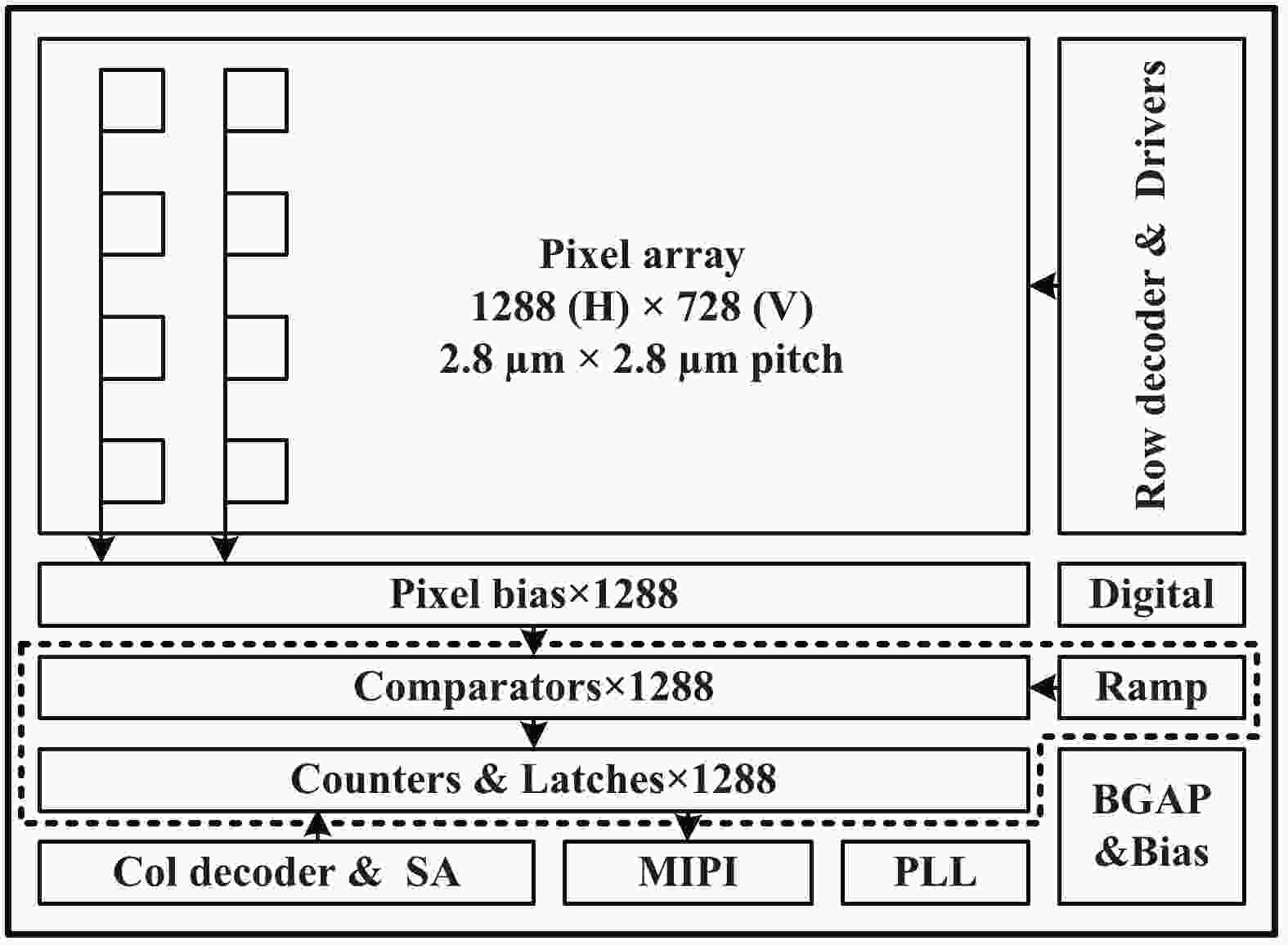
Fig. 1.  Block diagram of the overall architecture.

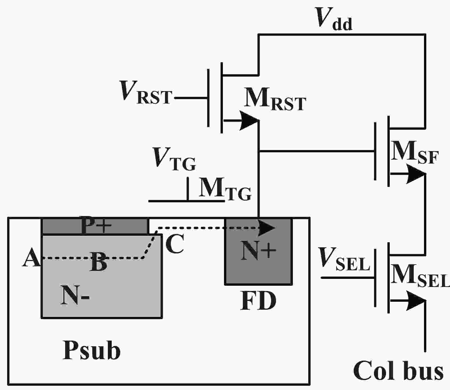
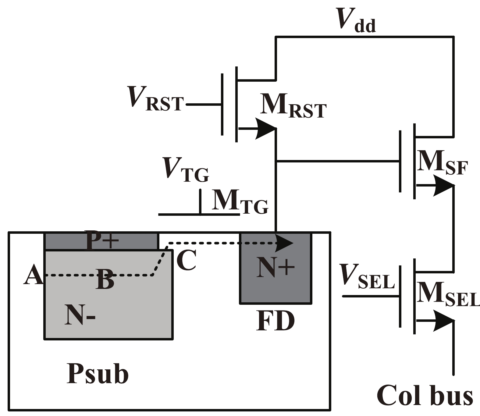
Fig. 2.  4T-PPD architecture.

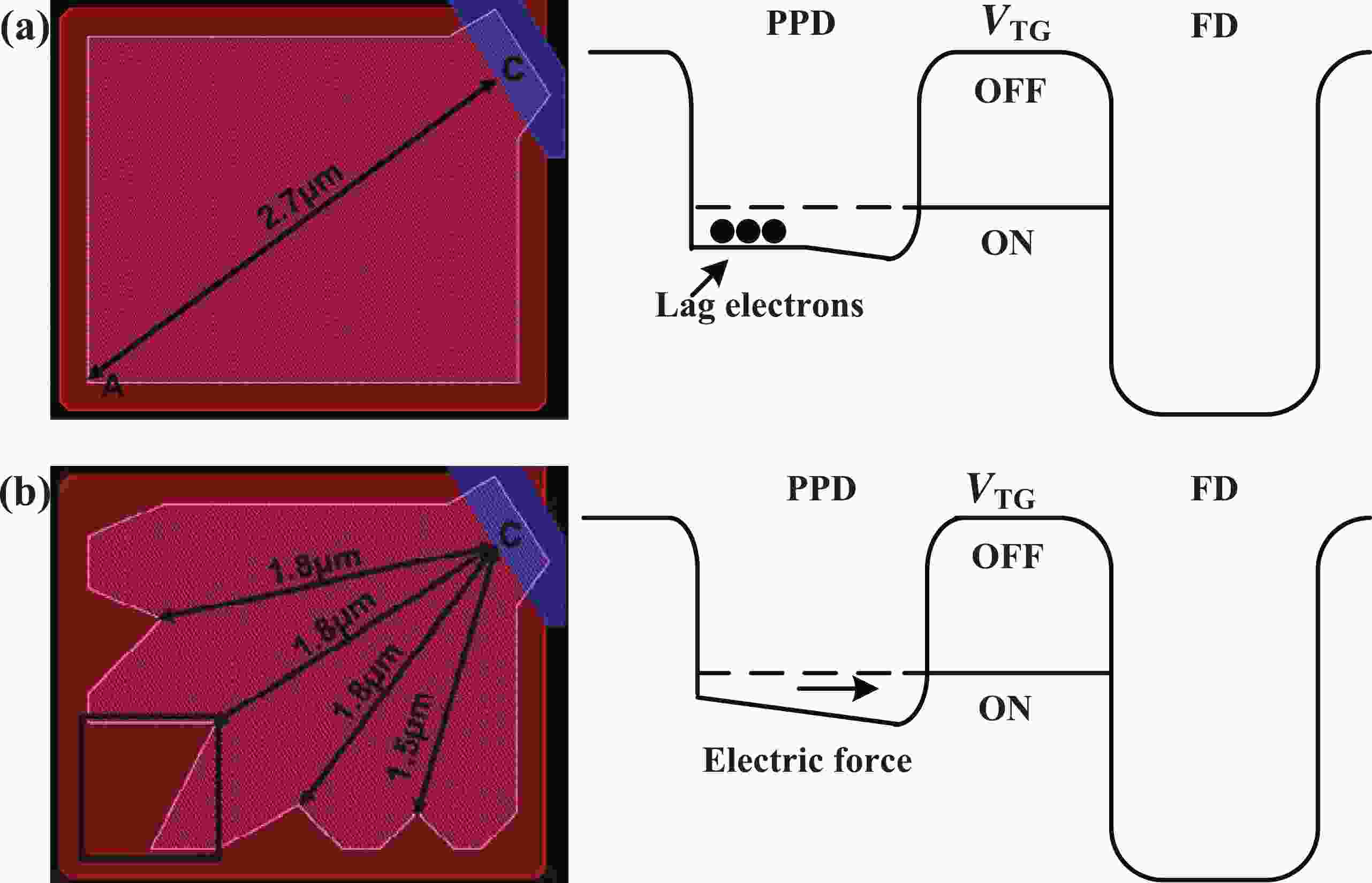
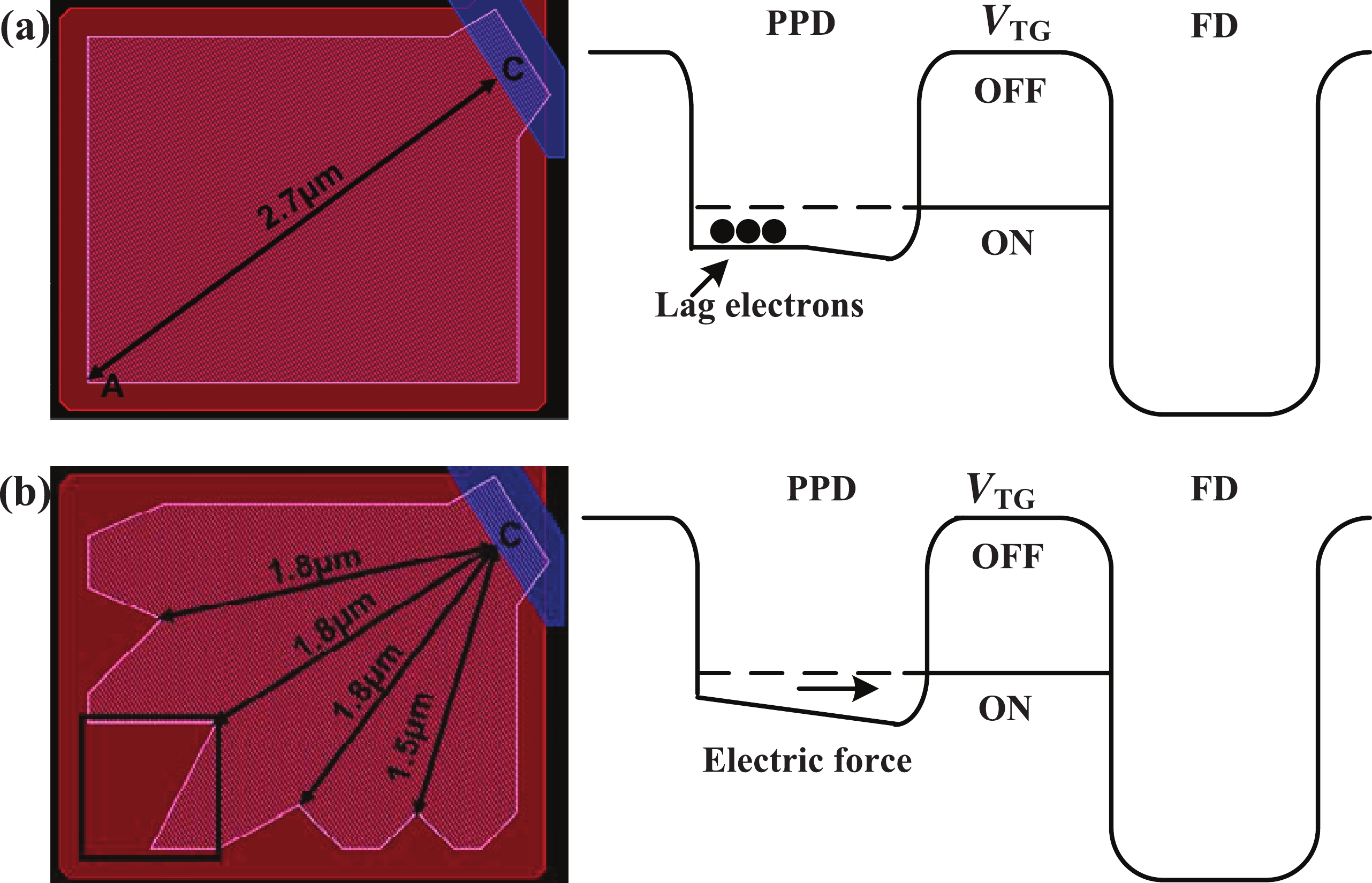
Fig. 3.  (Color online) PPD shape and potential profile: (a) conventional rectangle shaped, (b) proposed five-finger shaped.

Fig. 4.  Column circuit of the SS-ADC.

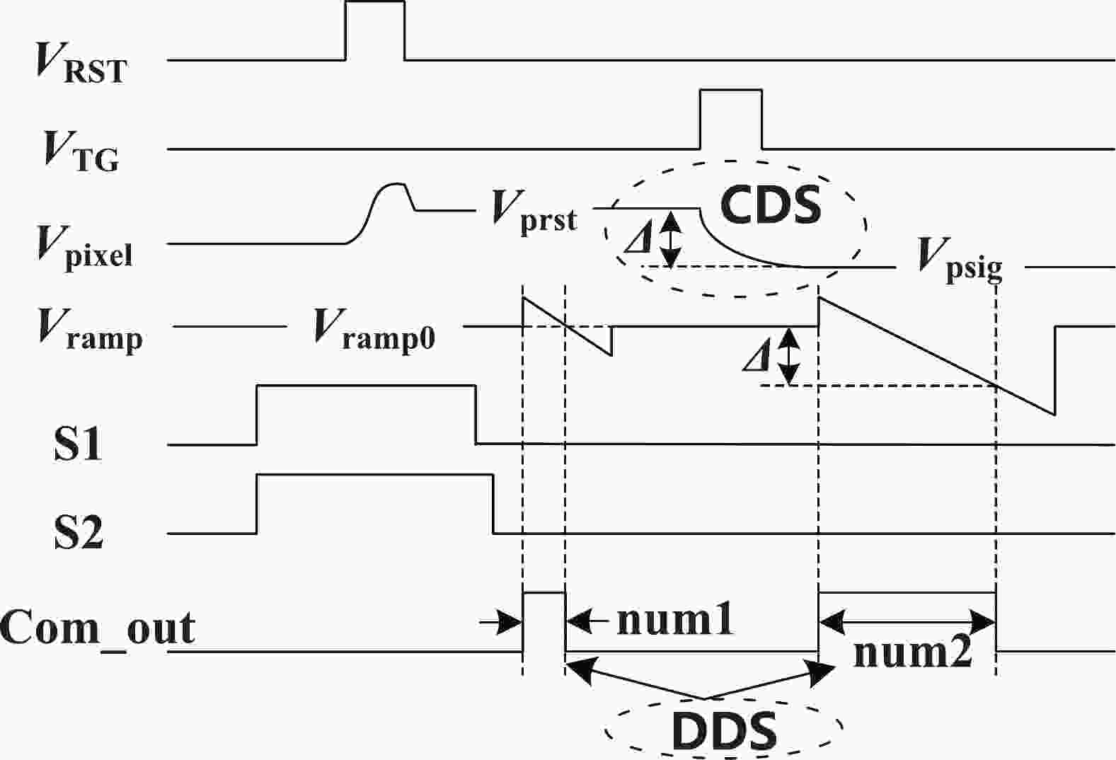
Fig. 5.  Timing diagram for dual correlated double sampling.

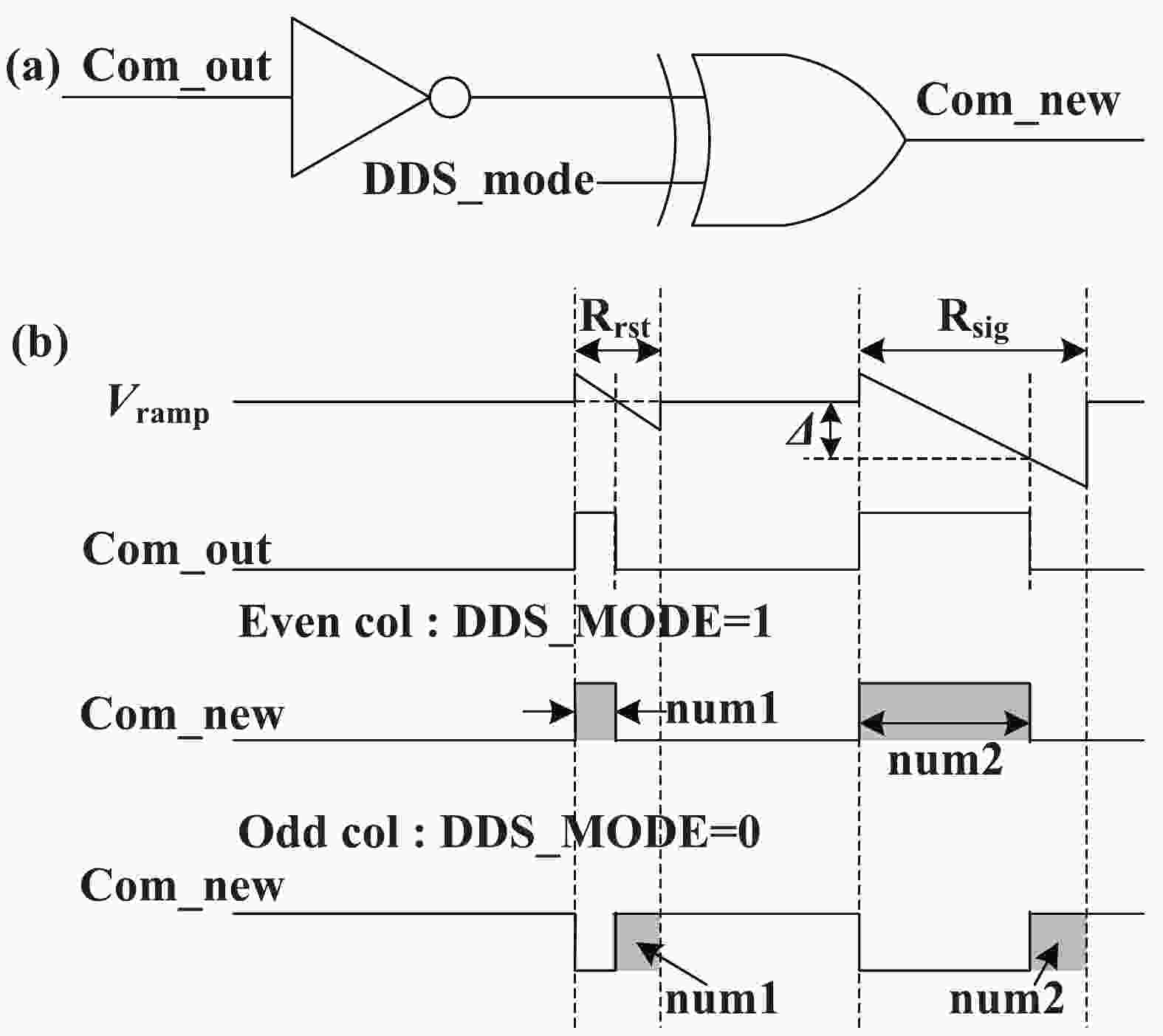
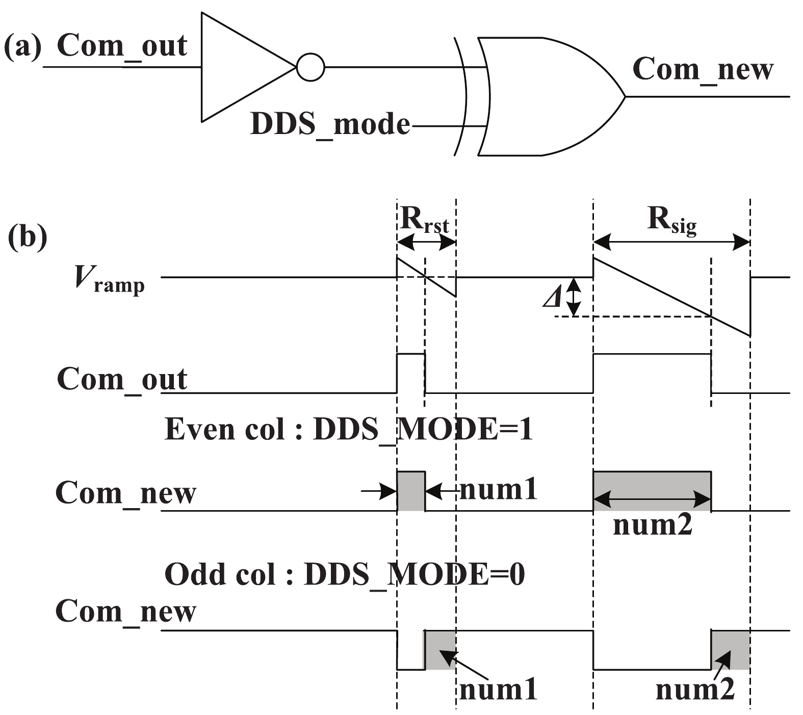
Fig. 6.  Dual-mode counting method: (a) circuit, (b) timing diagram.

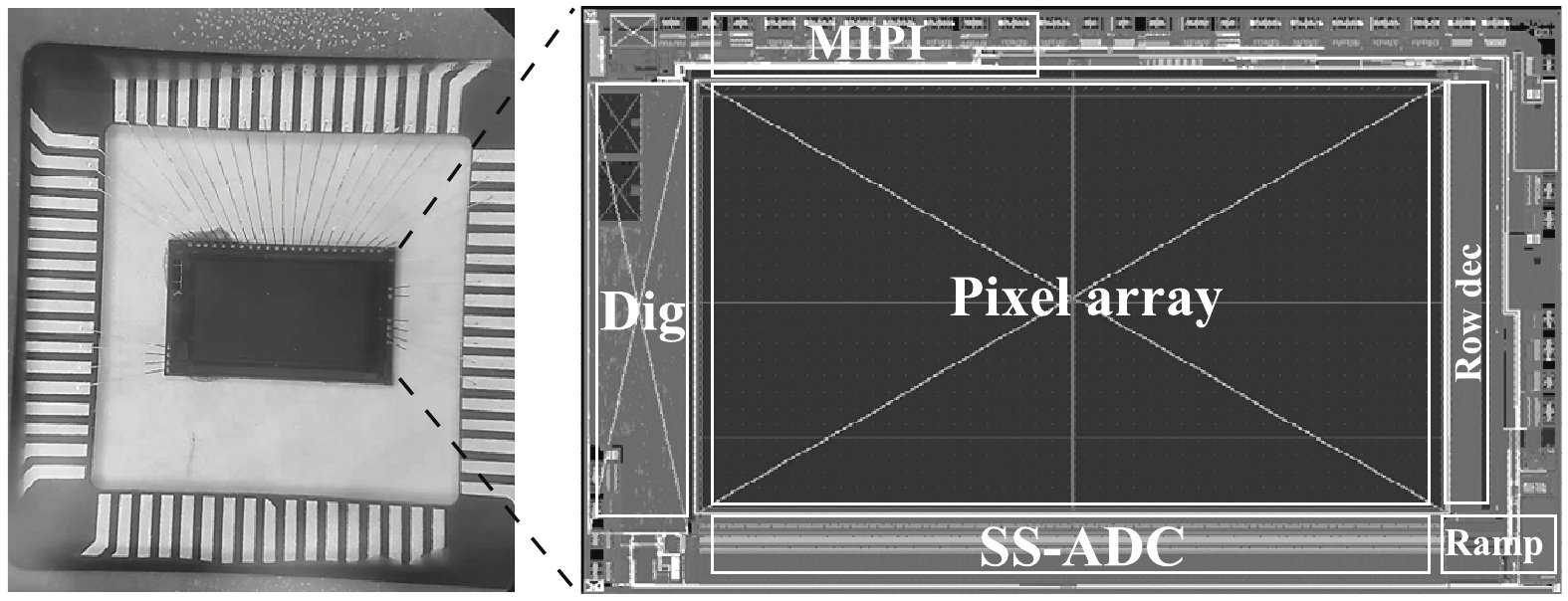
Fig. 7.  Chip photograph and layout.

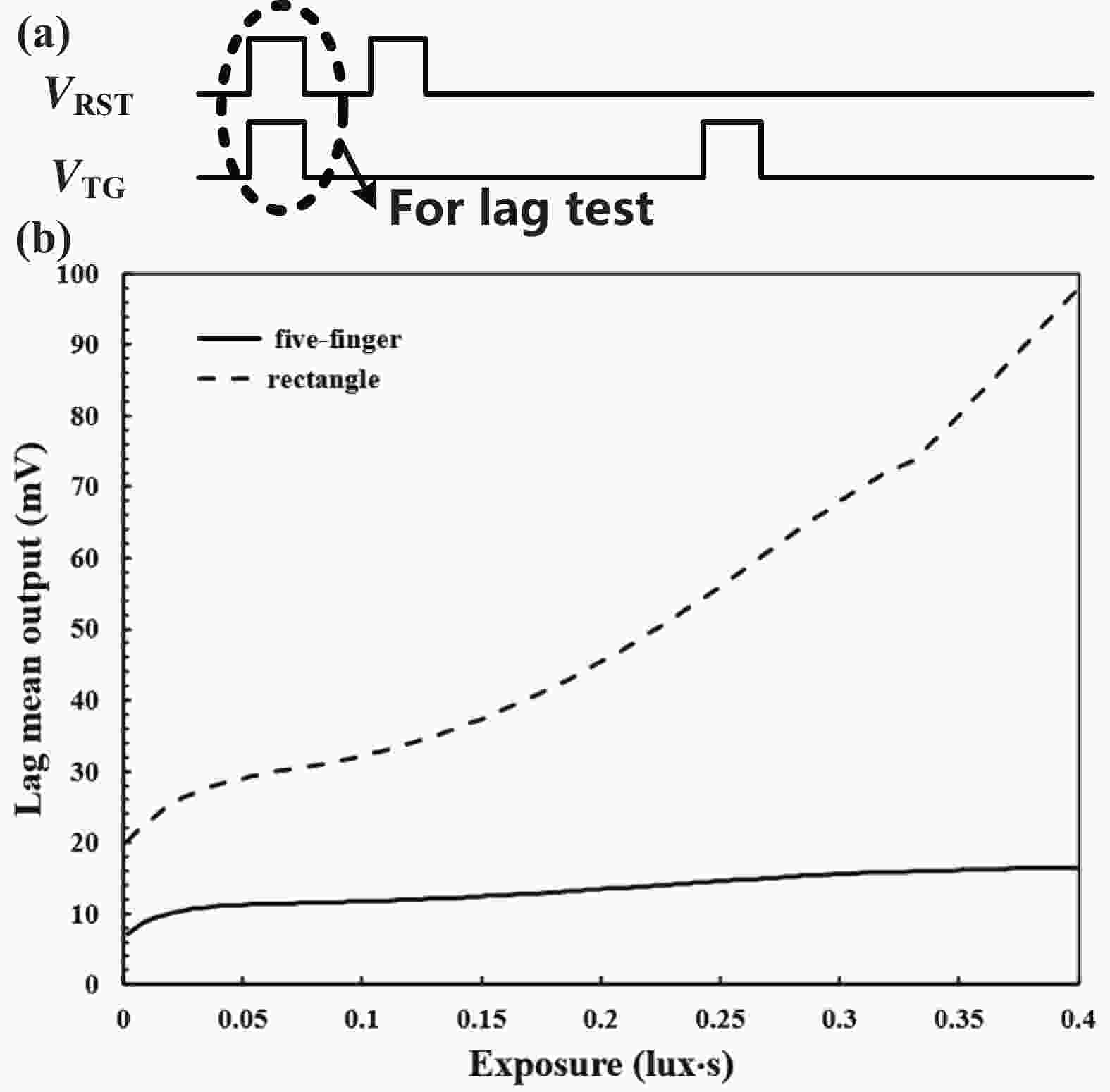
Fig. 8.  (a) Timing diagram for lag test. (b) Measured lag curves with different shaped PPD.

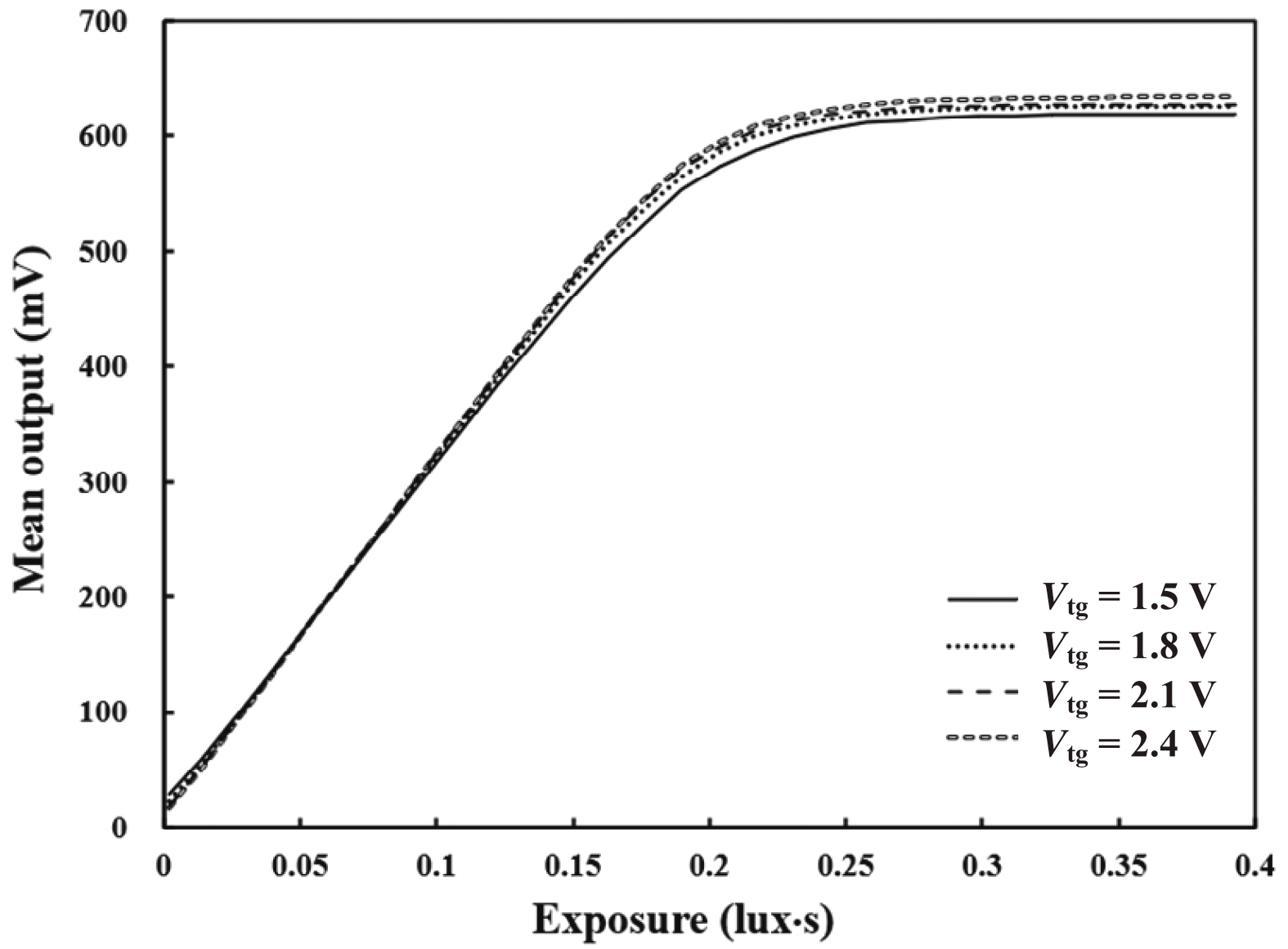
Fig. 9.  Measured photo response curves of five-finger shaped PPD with different transfer gate voltage.

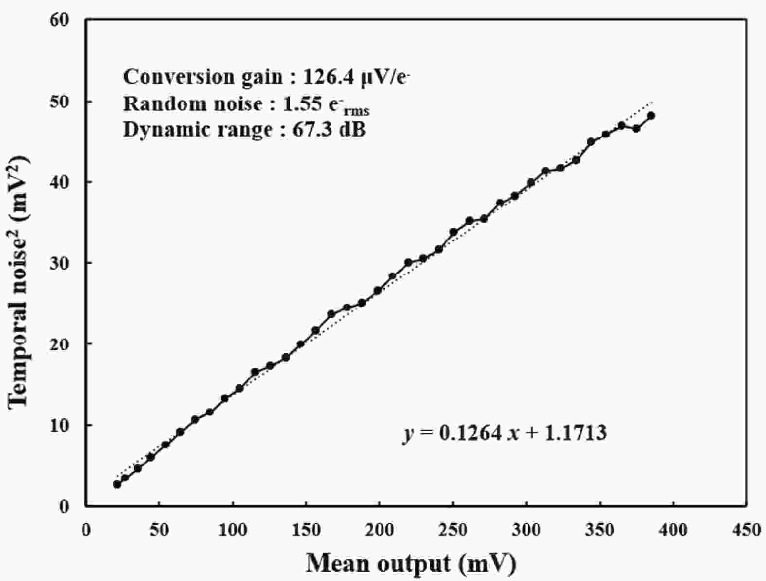
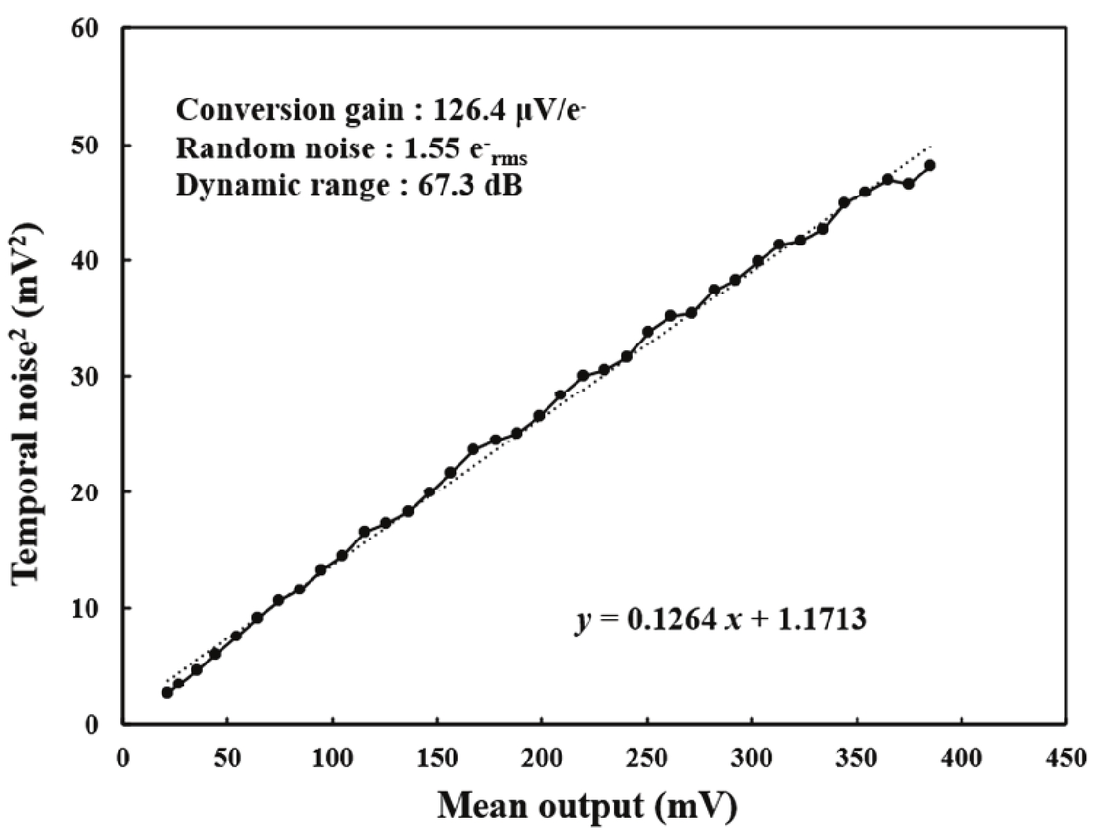
Fig. 10.  Measured photon transfer curve.

Fig. 11.  Captured image from the fabricated sensor.

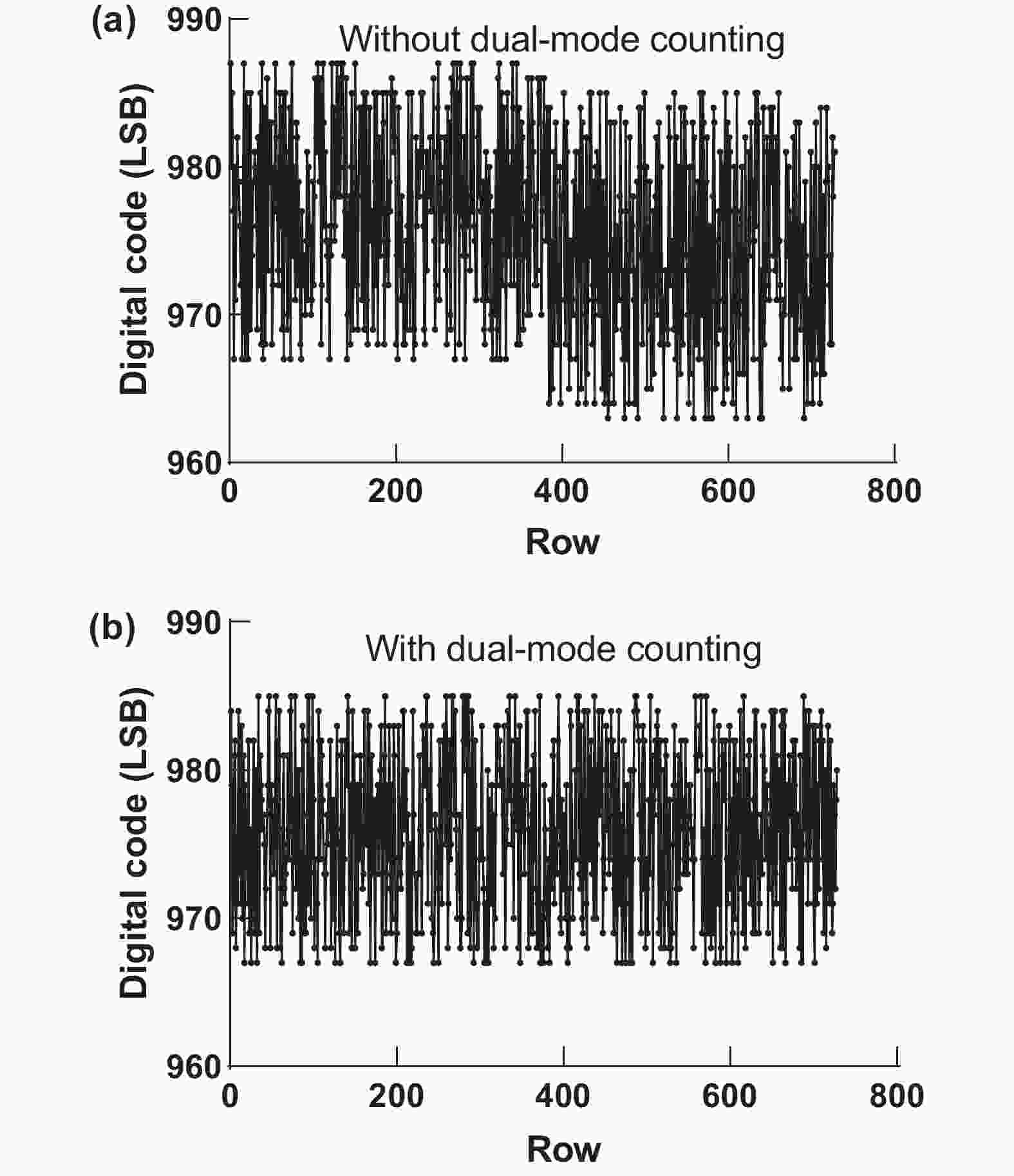
Fig. 12.  (a) Measured Digital codes of the 644th column without dual-mode counting. (b) Measured Digital codes of the 644th column with dual-mode counting.

Table 1.   Chip power consumption.

ParameterVoltage (V)Current (A)Power consumption (mW)
Pixel and analog1.510.3515.525
Digital1.216.9620.352
I/O1.80.030.054
Sum35.931
DownLoad: CSV

Table 2.   Comparison with other published CIS.

ParameterThis workJSSC[6]TCASI[17]Sensor[18]JSSC[4]
Process (nm)1101101109065
Pixel pitch (µm)2.85.06.55.64.0
Pixel type4T PPD4T PPD4T PPD4T PPDDigital
Pixel resolution1288 × 728640 × 480320 × 240128 × 128960 × 720128 × 128
Frame rate (fps)3015152283532
Power supply (V)1.5/1.23.3/1.80.93.3/1.52.8/1.50.5
Dynamic range (dB)67.3695068.966.742
Power consumption (mW)362.280.045540280.0088
Random noise (erms)1.555.583.73.25*3.73*416
FoM (e·nJ)1.982.723.3134.84.326.98
* For fair comparison, conversion gain is assumed by 126.4 μV/e.
DownLoad: CSV
[1]
Park I, Jo W, Park C, et al. A 640 × 640 fully dynamic CMOS image sensor for always-on operation. IEEE J Solid State Circuits, 2020, 55, 898 doi: 10.1109/JSSC.2019.2959486
[2]
Hsu T H, Chen Y R, Liu R S, et al. A 0.5-V real-time computational CMOS image sensor with programmable kernel for feature extraction. IEEE J Solid State Circuits, 2021, 56, 1588 doi: 10.1109/JSSC.2020.3034192
[3]
Hanson S, Foo Z, Blaauw D, et al. A 0.5 V sub-microwatt CMOS image sensor with pulse-width modulation read-out. IEEE J Solid State Circuits, 2010, 45, 759 doi: 10.1109/JSSC.2010.2040231
[4]
Couniot N, de Streel G, Botman F, et al. A 65 nm 0.5 V DPS CMOS image sensor with 17 pJ/Frame. Pixel and 42 dB dynamic range for ultra-low-power SoCs. IEEE J Solid State Circuits, 2015, 50, 2419 doi: 10.1109/JSSC.2015.2457897
[5]
Cho K B, Krymski A I, Fossum E R. A 1.5-V 550-μW 176 × 144 autonomous CMOS active pixel image sensor. IEEE Trans Electron Devices, 2003, 50, 96 doi: 10.1109/TED.2002.806475
[6]
Choi J, Shin J, Kang D W, et al. Always-on CMOS image sensor for mobile and wearable devices. IEEE J Solid State Circuits, 2016, 51, 130 doi: 10.1109/JSSC.2015.2470526
[7]
Nitta Y, Muramatsu Y, Amano K, et al. High-speed digital double sampling with analog CDS on column parallel ADC architecture for low-noise active pixel sensor. 2006 IEEE International Solid State Circuits Conference, 2006, 2024
[8]
Liu Q Y, Edward A, Kinyua M, et al. A low-power digitizer for back-illuminated 3-D-stacked CMOS image sensor readout with passing window and double auto-zeroing techniques. IEEE J Solid State Circuits, 2017, 52, 1591 doi: 10.1109/JSSC.2017.2661843
[9]
Park I, Park C, Cheon J, et al. A 76mW 500fps VGA CMOS image sensor with time-stretched single-slope ADCs achieving 1.95e- random noise. 2019 IEEE International Solid-State Circuits Conference, 2019, 100
[10]
Kim H J. 11-bit column-parallel single-slope ADC with first-step half-reference ramping scheme for high-speed CMOS image sensors. IEEE J Solid State Circuits, 2021, 56, 2132 doi: 10.1109/JSSC.2021.3059909
[11]
Shin B, Park S, Shin H. The effect of photodiode shape on charge transfer in CMOS image sensors. Solid State Electron, 2010, 54, 1416 doi: 10.1016/j.sse.2010.06.006
[12]
Xu Y, Theuwissen A J. Image lag analysis and photodiode shape optimization of 4T CMOS pixels. International Image Sensor Workshop, 2013
[13]
Cao X Z, Gäbler D, Lee C, et al. Design and optimization of large 4T pixel. International Image Sensor Workshop, 2015
[14]
Acerbi F, Garcia M M, Köklü G, et al. Transfer-gate region optimization and pinned-photodiode shaping for high-speed ToF applications. International Image Sensor Workshop, 2017
[15]
Millar T C, Sarhangnejad N, Katic N, et al. The effect of pinned photodiode shape on time-of-flight demodulation contrast. IEEE Trans Electron Devices, 2017, 64, 2244 doi: 10.1109/TED.2017.2677201
[16]
Kawahito S. Column-parallel ADCs for CMOS image sensors and their FoM-based evaluations. IEICE Trans Electron, 2018, E101.C, 444 doi: 10.1587/transele.E101.C.444
[17]
Nie K M, Zha W B, Shi X L, et al. A single slope ADC with row-wise noise reduction technique for CMOS image sensor. IEEE Trans Circuits Syst I, 2020, 67, 2873 doi: 10.1109/TCSI.2020.2979321
[18]
Park H, Yu C Z, Kim H, et al. Low power CMOS image sensors using two step single slope ADC with bandwidth-limited comparators & voltage range extended ramp generator for battery-limited application. IEEE Sens J, 2020, 20, 2831 doi: 10.1109/JSEN.2019.2957043
  • Search

    Advanced Search >>

    GET CITATION

    shu

    Export: BibTex EndNote

    Article Metrics

    Article views: 1959 Times PDF downloads: 167 Times Cited by: 0 Times

    History

    Received: 09 November 2021 Revised: 16 February 2022 Online: Accepted Manuscript: 13 May 2022Uncorrected proof: 19 May 2022Published: 01 August 2022

    Catalog

      Email This Article

      User name:
      Email:*请输入正确邮箱
      Code:*验证码错误
      Wenjing Xu, Jie Chen, Zhangqu Kuang, Li Zhou, Ming Chen, Chengbin Zhang. A low-power high-quality CMOS image sensor using 1.5 V 4T pinned photodiode and dual-CDS column-parallel single-slope ADC[J]. Journal of Semiconductors, 2022, 43(8): 082401. doi: 10.1088/1674-4926/43/8/082401 W J Xu, J Chen, Z Q Kuang, L Zhou, M Chen, C B Zhang. A low-power high-quality CMOS image sensor using 1.5 V 4T pinned photodiode and dual-CDS column-parallel single-slope ADC[J]. J. Semicond, 2022, 43(8): 082401. doi: 10.1088/1674-4926/43/8/082401Export: BibTex EndNote
      Citation:
      Wenjing Xu, Jie Chen, Zhangqu Kuang, Li Zhou, Ming Chen, Chengbin Zhang. A low-power high-quality CMOS image sensor using 1.5 V 4T pinned photodiode and dual-CDS column-parallel single-slope ADC[J]. Journal of Semiconductors, 2022, 43(8): 082401. doi: 10.1088/1674-4926/43/8/082401

      W J Xu, J Chen, Z Q Kuang, L Zhou, M Chen, C B Zhang. A low-power high-quality CMOS image sensor using 1.5 V 4T pinned photodiode and dual-CDS column-parallel single-slope ADC[J]. J. Semicond, 2022, 43(8): 082401. doi: 10.1088/1674-4926/43/8/082401
      Export: BibTex EndNote

      A low-power high-quality CMOS image sensor using 1.5 V 4T pinned photodiode and dual-CDS column-parallel single-slope ADC

      doi: 10.1088/1674-4926/43/8/082401
      More Information
      • Author Bio:

        Wenjing Xu received her B.E. and M.E. from Tianjin University, China, in 2010 and 2013, respectively. She is currently working towards a PhD at the Institute of Microelectronics of Chinese Academy of Science. Her research interests are CMOS image sensors and analog circuit design

        Jie Chen received his B.E. degree from the Harbin Engineering University, Harbin, China in 1986, and the M.E. and PhD degrees from the University of Electro-Communications (UEC), Tokyo, Japan in 1991 and 1994, respectively. In 2001, he was selected as a scientist of ‘‘100 Talents Program’’ by Chinese Academy of Sciences (CAS). He is now a Director Professor of the Institute of Analog Integrated Circuits and Signal Processing Microelectronics, CAS and a Professor of the Graduate School of CAS. His current research interests include SOC design for software-defined-radio (SDR), digital communications (CDMA and OFDM) and data compression

      • Corresponding author: jchen@ime.ac.cn
      • Received Date: 2021-11-09
      • Revised Date: 2022-02-16
      • Available Online: 2022-05-13

      Catalog

        /

        DownLoad:  Full-Size Img  PowerPoint
        Return
        Return