REVIEWS

The twisted two-dimensional ferroelectrics

Xinhao Zhang1, 2 and Bo Peng1, 2,

+ Author Affiliations

 Corresponding author: Bo Peng, bo_peng@uestc.edu.cn

PDF

Turn off MathJax

Abstract: Since the beginning of research on two-dimensional (2D) materials, a few numbers of 2D ferroelectric materials have been predicted or experimentally confirmed, but 2D ferroelectrics as necessary functional materials are greatly important in developing future electronic devices. Recent breakthroughs in 2D ferroelectric materials are impressive, and the physical and structural properties of twisted 2D ferroelectrics, a new type of ferroelectric structure by rotating alternating monolayers to form an angle with each other, have attracted widespread interest and discussion. Here, we review the latest research on twisted 2D ferroelectrics, including Bernal-stacked bilayer graphene/BN, bilayer boron nitride, and transition metal dichalcogenides. Finally, we prospect the development of twisted 2D ferroelectrics and discuss the challenges and future of 2D ferroelectric materials.

Key words: magic anglemultiferroicferromagneticelectric polarizationlong-range


[1]
Chai X J, Jiang J, Zhang Q H, et al. Nonvolatile ferroelectric field-effect transistors. Nat Commun, 2020, 11, 2811 doi: 10.1038/s41467-020-16623-9
[2]
Naber R C G, Tanase C, Blom P W M, et al. High-performance solution-processed polymer ferroelectric field-effect transistors. Nature Mater, 2005, 4, 243 doi: 10.1038/nmat1329
[3]
Si M W, Saha A K, Gao S J, et al. A ferroelectric semiconductor field-effect transistor. Nat Electron, 2019, 2, 580 doi: 10.1038/s41928-019-0338-7
[4]
Si M W, Liao P Y, Qiu G, et al. Ferroelectric field-effect transistors based on MoS2 and CuInP2S6 two-dimensional van der waals heterostructure. ACS Nano, 2018, 12, 6700 doi: 10.1021/acsnano.8b01810
[5]
Wan S Y, Li Y, Li W, et al. Nonvolatile ferroelectric memory effect in ultrathin α-In2Se3. Adv Funct Mater, 2019, 29, 1808606 doi: 10.1002/adfm.201808606
[6]
Luo Z D, Yang M M, Liu Y, et al. Emerging opportunities for 2D semiconductor/ferroelectric transistor-structure devices. Adv Mater, 2021, 33, 2005620 doi: 10.1002/adma.202005620
[7]
Wu G, Tian B, Liu L, et al. Programmable transition metal dichalcogenide homojunctions controlled by nonvolatile ferroelectric domains. Nat Electron, 2020, 3, 43 doi: 10.1038/s41928-019-0350-y
[8]
Luo Z D, Xia X, Yang M M, et al. Artificial optoelectronic synapses based on ferroelectric field-effect enabled 2D transition metal dichalcogenide memristive transistors. ACS Nano, 2020, 14, 746 doi: 10.1021/acsnano.9b07687
[9]
Lv L, Zhuge F W, Xie F J, et al. Reconfigurable two-dimensional optoelectronic devices enabled by local ferroelectric polarization. Nat Commun, 2019, 10, 3331 doi: 10.1038/s41467-019-11328-0
[10]
Li T, Sharma P, Lipatov A, et al. Polarization-mediated modulation of electronic and transport properties of hybrid MoS2-BaTiO3-SrRuO3 tunnel junctions. Nano Lett, 2017, 17, 922 doi: 10.1021/acs.nanolett.6b04247
[11]
Wang X, Wang P, Wang J, et al. Ultrasensitive and broadband MoS2 photodetector driven by ferroelectrics. Adv Mater, 2015, 27, 6575 doi: 10.1002/adma.201503340
[12]
Lipatov A, Sharma P, Gruverman A, et al. Optoelectrical molybdenum disulfide (MoS2)—Ferroelectric memories. ACS Nano, 2015, 9, 8089 doi: 10.1021/acsnano.5b02078
[13]
Lee H S, Min S W, Park M K, et al. MoS2 Nanosheets for top-gate nonvolatile memory transistor channel. Small, 2012, 8, 3111 doi: 10.1002/smll.201200752
[14]
Scott J F, Paz de Araujo C A. Ferroelectric memories. Science, 1989, 246, 1400 doi: 10.1126/science.246.4936.1400
[15]
Jiang A Q, Wang C, Jin K J, et al. A resistive memory in semiconducting BiFeO3 thin-film capacitors. Adv Mater, 2011, 23, 1277 doi: 10.1002/adma.201004317
[16]
Ishiwara H. Ferroelectric random access memories. J Nanosci Nanotechnol, 2012, 12, 7619 doi: 10.1166/jnn.2012.6651
[17]
Mikolajick T, Slesazeck S, Park M H, et al. Ferroelectric hafnium oxide for ferroelectric random-access memories and ferroelectric field-effect transistors. MRS Bull, 2018, 43, 340 doi: 10.1557/mrs.2018.92
[18]
Hyun S D, Park H W, Park M H, et al. Field-induced ferroelectric Hf1– xZr xO2 thin films for high-k dynamic random access memory. Adv Electron Mater, 2020, 6, 2000631 doi: 10.1002/aelm.202000631
[19]
Wang S, Liu L, Gan L, et al. Two-dimensional ferroelectric channel transistors integrating ultra-fast memory and neural computing. Nat Commun, 2021, 12, 1 doi: 10.1038/s41467-020-20314-w
[20]
Dai M, Li K, Wang F, et al. Intrinsic dipole coupling in 2D van der Waals ferroelectrics for gate-controlled switchable rectifier. Adv Electron Mater, 2020, 6, 1900975 doi: 10.1002/aelm.201900975
[21]
Wan S Y, Li Y, Li W, et al. Room-temperature ferroelectricity and a switchable diode effect in two-dimensional α-In2Se3 thin layers. Nanoscale, 2018, 10, 14885 doi: 10.1039/C8NR04422H
[22]
Poh S M, Tan S J R, Wang H, et al. Molecular-beam epitaxy of two-dimensional In2Se3 and its giant electroresistance switching in ferroresistive memory junction. Nano Lett, 2018, 18, 6340 doi: 10.1021/acs.nanolett.8b02688
[23]
Yoon J, Hong S, Song Y W, et al. Understanding tunneling electroresistance effect through potential profile in Pt/Hf0.5Zr0.5O2/TiN ferroelectric tunnel junction memory. Appl Phys Lett, 2019, 115, 153502 doi: 10.1063/1.5119948
[24]
Goh Y, Jeon S. Enhanced tunneling electroresistance effects in HfZrO-based ferroelectric tunnel junctions by high-pressure nitrogen annealing. Appl Phys Lett, 2018, 113, 052905 doi: 10.1063/1.5040031
[25]
Ambriz-Vargas F, Kolhatkar G, Broyer M, et al. A complementary metal oxide semiconductor process-compatible ferroelectric tunnel junction. ACS Appl Mater Interfaces, 2017, 9, 13262 doi: 10.1021/acsami.6b16173
[26]
Park J Y, Yang K, Lee D H, et al. A perspective on semiconductor devices based on fluorite-structured ferroelectrics from the materials–device integration perspective. J Appl Phys, 2020, 128, 240904 doi: 10.1063/5.0035542
[27]
Xi Z, Ruan J, Li C, et al. Giant tunnelling electroresistance in metal/ferroelectric/semiconductor tunnel junctions by engineering the Schottky barrier. Nat Commun, 2017, 8, 1 doi: 10.1038/s41467-016-0009-6
[28]
Xue F, He X, Liu W, et al. Optoelectronic ferroelectric domain‐wall memories made from a single Van Der Waals ferroelectric. Adv Funct Mater, 2020, 30, 2004206 doi: 10.1002/adfm.202004206
[29]
Xu K, Jiang W, Gao X S, et al. Optical control of ferroelectric switching and multifunctional devices based on van der Waals ferroelectric semiconductors. Nanoscale, 2020, 12, 23488 doi: 10.1039/D0NR06872A
[30]
Wang L, Wang X, Zhang Y, et al. Exploring ferroelectric switching in α-In2Se3 for neuromorphic computing. Adv Funct Mater, 2020, 30, 2004609 doi: 10.1002/adfm.202004609
[31]
Zhang Y S, Wang L, Chen H, et al. Analog and digital mode α-In2Se3 memristive devices for neuromorphic and memory applications. Adv Electron Mater, 2021, 7, 2100609 doi: 10.1002/aelm.202100609
[32]
Kwon K C, Zhang Y S, Wang L, et al. In-plane ferroelectric tin monosulfide and its application in a ferroelectric analog synaptic device. ACS Nano, 2020, 14, 7628 doi: 10.1021/acsnano.0c03869
[33]
Bian J H, Cao Z Y, Zhou P. Neuromorphic computing: Devices, hardware, and system application facilitated by two-dimensional materials. Appl Phys Rev, 2021, 8, 041313 doi: 10.1063/5.0067352
[34]
Dai M, Wang Z, Wang F, et al. Two-dimensional van der Waals materials with aligned in-plane polarization and large piezoelectric effect for self-powered piezoelectric sensors. Nano Lett, 2019, 19, 5410 doi: 10.1021/acs.nanolett.9b01907
[35]
Kim H J, Schanze K. Introducing ACS applied electronic materials. ACS Appl Electron Mater, 2019, 1, 1 doi: 10.1021/acsaelm.8b00087
[36]
Xue F, Zhang J, Hu W, et al. Multidirection piezoelectricity in mono- and multilayered hexagonal α-In2Se3. ACS Nano, 2018, 12, 4976 doi: 10.1021/acsnano.8b02152
[37]
Scott J F. Applications of modern ferroelectrics. Science, 2007, 315, 954 doi: 10.1126/science.1129564
[38]
Prateek, Thakur V K, Gupta R K. Recent progress on ferroelectric polymer-based nanocomposites for high energy density capacitors: Synthesis, dielectric properties, and future aspects. Chem Rev, 2016, 116, 4260 doi: 10.1021/acs.chemrev.5b00495
[39]
Valasek J. Piezo-electric and allied phenomena in rochelle salt. Phys Rev, 1921, 17, 475 doi: 10.1103/PhysRev.17.475
[40]
Junquera J, Ghosez P. Critical thickness for ferroelectricity in perovskite ultrathin films. Nature, 2003, 422, 506 doi: 10.1038/nature01501
[41]
Fong D D, Stephenson G B, Streiffer S K, et al. Ferroelectricity in ultrathin perovskite films. Science, 2004, 304, 1650 doi: 10.1126/science.1098252
[42]
Novoselov K S, Geim A K, Morozov S V, et al. Electric field effect in atomically thin carbon films. Science, 2004, 306, 666 doi: 10.1126/science.1102896
[43]
Lee D, Lu H, Gu Y, et al. Emergence of room-temperature ferroelectricity at reduced dimensions. Science, 2015, 349, 1314 doi: 10.1126/science.aaa6442
[44]
Yuan S G, Luo X, Chan H L, et al. Room-temperature ferroelectricity in MoTe2 down to the atomic monolayer limit. Nat Commun, 2019, 10, 1775 doi: 10.1038/s41467-019-09669-x
[45]
Zhou Y, Wu D, Zhu Y H, et al. Out-of-plane piezoelectricity and ferroelectricity in layered α-In2Se3 nanoflakes. Nano Lett, 2017, 17, 5508 doi: 10.1021/acs.nanolett.7b02198
[46]
Cui C, Hu W J, Yan X, et al. Intercorrelated in-plane and out-of-plane ferroelectricity in ultrathin two-dimensional layered semiconductor In2Se3. Nano Lett, 2018, 18, 1253 doi: 10.1021/acs.nanolett.7b04852
[47]
Xiao J, Zhu H, Wang Y, et al. Intrinsic two-dimensional ferroelectricity with dipole locking. Phys Rev Lett, 2018, 120, 227601 doi: 10.1103/PhysRevLett.120.227601
[48]
Io W F, Yuan S G, Pang S Y, et al. Temperature- and thickness-dependence of robust out-of-plane ferroelectricity in CVD grown ultrathin van der Waals α-In2Se3 layers. Nano Res, 2020, 13, 1897 doi: 10.1007/s12274-020-2640-0
[49]
Zheng C, Yu L, Zhu L, et al. Room temperature in-plane ferroelectricity in van der Waals In2Se3. Sci Adv, 2018, 4, eaar7720 doi: 10.1126/sciadv.aar7720
[50]
Lv B, Yan Z, Xue W, et al. Layer-dependent ferroelectricity in 2H-stacked few-layer α-In2Se3. Mater Horiz, 2021, 8, 1472 doi: 10.1039/D0MH01863E
[51]
Belianinov A, He Q, Dziaugys A, et al. CuInP2S6 room temperature layered ferroelectric. Nano Lett, 2015, 15, 3808 doi: 10.1021/acs.nanolett.5b00491
[52]
Liu F C, You L, Seyler K L, et al. Room-temperature ferroelectricity in CuInP2S6 ultrathin flakes. Nat Commun, 2016, 7, 12357 doi: 10.1038/ncomms12357
[53]
Chang K, Liu J, Lin H, et al. Discovery of robust in-plane ferroelectricity in atomic-thick SnTe. Science, 2016, 353, 274 doi: 10.1126/science.aad8609
[54]
Fei Z, Zhao W, Palomaki T A, et al. Ferroelectric switching of a two-dimensional metal. Nature, 2018, 560, 336 doi: 10.1038/s41586-018-0336-3
[55]
You L, Liu F C, Li H S, et al. In-plane ferroelectricity in thin flakes of van der waals hybrid perovskite. Adv Mater, 2018, 30, 1803249 doi: 10.1002/adma.201803249
[56]
Geim A K, Grigorieva I V. Van der Waals heterostructures. Nature, 2013, 499, 419 doi: 10.1038/nature12385
[57]
Suárez Morell E, Correa J D, Vargas P, et al. Flat bands in slightly twisted bilayer graphene: Tight-binding calculations. Phys Rev B, 2010, 82, 121407 doi: 10.1103/PhysRevB.82.121407
[58]
Yankowitz M, Chen S, Polshyn H, et al. Tuning superconductivity in twisted bilayer graphene. Science, 2019, 363, 1059 doi: 10.1126/science.aav1910
[59]
Wang L, Shih E M, Ghiotto A, et al. Correlated electronic phases in twisted bilayer transition metal dichalcogenides. Nat Mater, 2020, 19, 861 doi: 10.1038/s41563-020-0708-6
[60]
Tang Y H, Li L Z, Li T X, et al. Simulation of Hubbard model physics in WSe2/WS2 moiré superlattices. Nature, 2020, 579, 353 doi: 10.1038/s41586-020-2085-3
[61]
Shen C, Chu Y, Wu Q, et al. Correlated states in twisted double bilayer graphene. Nat Phys, 2020, 16, 520 doi: 10.1038/s41567-020-0825-9
[62]
Sharpe A L, Fox E J, Barnard A W, et al. Emergent ferromagnetism near three-quarters filling in twisted bilayer graphene. Science, 2019, 365, 605 doi: 10.1126/science.aaw3780
[63]
Serlin M, Tschirhart C L, Polshyn H, et al. Intrinsic quantized anomalous Hall effect in a moiré heterostructure. Science, 2020, 367, 900 doi: 10.1126/science.aay5533
[64]
Regan E C, Wang D, Jin C, et al. Mott and generalized Wigner crystal states in WSe2/WS2 moiré superlattices. Nature, 2020, 579, 359 doi: 10.1038/s41586-020-2092-4
[65]
Liu X, Hao Z, Khalaf E, et al. Tunable spin-polarized correlated states in twisted double bilayer graphene. Nature, 2020, 583, 221 doi: 10.1038/s41586-020-2458-7
[66]
Li G H, Luican A, Lopes dos Santos J M B, et al. Observation of Van Hove singularities in twisted graphene layers. Nat Phys, 2010, 6, 109 doi: 10.1038/nphys1463
[67]
Chen G R, Sharpe A L, Fox E J, et al. Tunable correlated Chern insulator and ferromagnetism in a moiré superlattice. Nature, 2020, 579, 56 doi: 10.1038/s41586-020-2049-7
[68]
Chen G R, Jiang L L, Wu S, et al. Evidence of a gate-tunable Mott insulator in a trilayer graphene moiré superlattice. Nat Phys, 2019, 15, 237 doi: 10.1038/s41567-018-0387-2
[69]
Cao Y, Rodan-Legrain D, Rubies-Bigorda O, et al. Tunable correlated states and spin-polarized phases in twisted bilayer-bilayer graphene. Nature, 2020, 583, 215 doi: 10.1038/s41586-020-2260-6
[70]
Cao Y, Fatemi V, Fang S A, et al. Unconventional superconductivity in magic-angle graphene superlattices. Nature, 2018, 556, 43 doi: 10.1038/nature26160
[71]
Cao Y, Fatemi V, Demir A, et al. Correlated insulator behaviour at half-filling in magic-angle graphene superlattices. Nature, 2018, 556, 80 doi: 10.1038/nature26154
[72]
Burg G W, Zhu J H, Taniguchi T, et al. Correlated insulating states in twisted double bilayer graphene. Phys Rev Lett, 2019, 123, 197702 doi: 10.1103/PhysRevLett.123.197702
[73]
Bistritzer R, MacDonald A H. Moiré bands in twisted double-layer graphene. PNAS, 2011, 108, 12233 doi: 10.1073/pnas.1108174108
[74]
Zheng Z R, Ma Q, Bi Z, et al. Unconventional ferroelectricity in moiré heterostructures. Nature, 2020, 588, 71 doi: 10.1038/s41586-020-2970-9
[75]
Yasuda K, Wang X, Watanabe K, et al. Stacking-engineered ferroelectricity in bilayer boron nitride. Science, 2021, 372, 1458 doi: 10.1126/science.abd3230
[76]
Wang X, Yasuda K, Zhang Y, et al. Interfacial ferroelectricity in rhombohedral-stacked bilayer transition metal dichalcogenides. Nat Nanotechnol, 2022, 17, 367 doi: 10.1038/s41565-021-01059-z
[77]
Ding W J, Zhu J B, Wang Z, et al. Prediction of intrinsic two-dimensional ferroelectrics in In2Se3 and other III2-VI3 van der Waals materials. Nat Commun, 2017, 8, 14956 doi: 10.1038/ncomms14956
[78]
Ishiwara H. Current status and prospects of FET-type ferroelectric memories. International Electron Devices Meeting, 2001, 1, 725 doi: 10.1109/IEDM.2001.979615
[79]
Ma T P, Han J P. Why is nonvolatile ferroelectric memory field-effect transistor still elusive. IEEE Electron Device Lett, 2002, 23, 386 doi: 10.1109/LED.2002.1015207
[80]
Yurchuk E, Muller J, Muller S, et al. Charge-trapping phenomena in HfO2-based FeFET-type nonvolatile memories. IEEE Trans Electron Devices, 2016, 63, 3501 doi: 10.1109/TED.2016.2588439
[81]
Simon A, Ravez J, Maisonneuve V, et al. Paraelectric-ferroelectric transition in the lamellar thiophosphate CuInP2S6. Chem Mater, 1994, 6, 1575 doi: 10.1021/cm00045a016
[82]
Maisonneuve V, Reau J M, Dong M, et al. Ionic conductivity in ferroic CuInP2S6 and CuCrP2S6. Ferroelectrics, 1997, 196, 257 doi: 10.1080/00150199708224175
[83]
Kim H J, Kang S H, Hamada I, et al. Origins of the structural phase transitions in MoTe2 and WTe2. Phys Rev B, 2017, 95, 180101 doi: 10.1103/PhysRevB.95.180101
[84]
Keum D H, Cho S, Kim J H, et al. Bandgap opening in few-layered monoclinic MoTe2. Nat Phys, 2015, 11, 482 doi: 10.1038/nphys3314
[85]
Qian X F, Liu J W, Fu L, et al. Quantum spin Hall effect in two-dimensional transition metal dichalcogenides. Science, 2014, 346, 1344 doi: 10.1126/science.1256815
[86]
Eda G, Fujita T, Yamaguchi H, et al. Coherent atomic and electronic heterostructures of single-layer MoS2. ACS Nano, 2012, 6, 7311 doi: 10.1021/nn302422x
[87]
Bruyer E, Di Sante D, Barone P, et al. Possibility of combining ferroelectricity and Rashba-like spin splitting in monolayers of the 1 T-type transition-metal dichalcogenides MX2 (M = Mo, W; X = S, Se, Te). Phys Rev B, 2016, 94, 195402 doi: 10.1103/PhysRevB.94.195402
[88]
Shirodkar S N, Waghmare U V. Emergence of ferroelectricity at a metal-semiconductor transition in a 1T monolayer of MoS2. Phys Rev Lett, 2014, 112, 157601 doi: 10.1103/PhysRevLett.112.157601
[89]
Yang Q, Wu M H, Li J. Origin of two-dimensional vertical ferroelectricity in WTe2 bilayer and multilayer. J Phys Chem Lett, 2018, 9, 7160 doi: 10.1021/acs.jpclett.8b03654
[90]
Castro Neto A H, Guinea F, Peres N M R, et al. The electronic properties of graphene. Rev Mod Phys, 2009, 81, 109 doi: 10.1103/RevModPhys.81.109
[91]
de la Barrera S C, Aronson S, Zheng Z R, et al. Cascade of isospin phase transitions in Bernal-stacked bilayer graphene at zero magnetic field. Nat Phys, 2022, 18, 771 doi: 10.1038/s41567-022-01616-w
[92]
Constantinescu G, Kuc A, Heine T. Stacking in bulk and bilayer hexagonal boron nitride. Phys Rev Lett, 2013, 111, 036104 doi: 10.1103/PhysRevLett.111.036104
[93]
Park H J, Cha J, Choi M, et al. One-dimensional hexagonal boron nitride conducting channel. Sci Adv, 2020, 6, eaay4958 doi: 10.1126/sciadv.aay4958
[94]
Li L, Wu M H. Binary compound bilayer and multilayer with vertical polarizations: Two-dimensional ferroelectrics, multiferroics, and nanogenerators. ACS Nano, 2017, 11, 6382 doi: 10.1021/acsnano.7b02756
[95]
Towle L C, Oberbeck V, Brown B E, et al. Molybdenum diselenide: Rhombohedral high pressure-high temperature polymorph. Science, 1966, 154, 895 doi: 10.1126/science.154.3751.895
[96]
Weston A, Zou Y, Enaldiev V, et al. Atomic reconstruction in twisted bilayers of transition metal dichalcogenides. Nat Nanotechnol, 2020, 15, 592 doi: 10.1038/s41565-020-0682-9
[97]
Cui C J, Xue F, Hu W J, et al. Two-dimensional materials with piezoelectric and ferroelectric functionalities. npj 2D Mater Appl, 2018, 2, 18 doi: 10.1038/s41699-018-0063-5
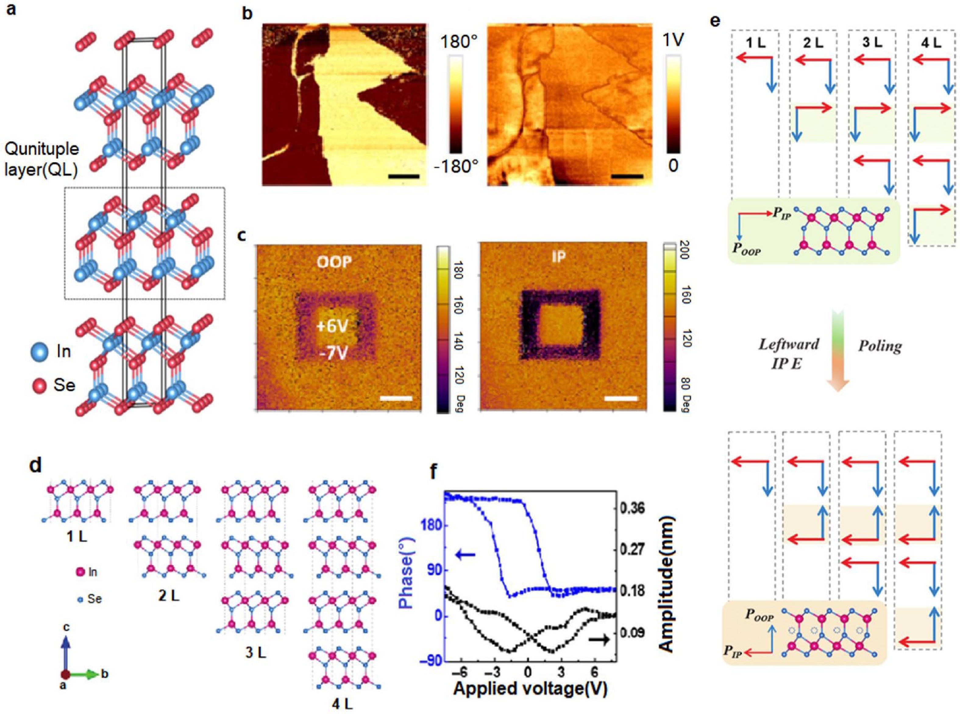
Fig. 1.  (Color online) (a) Schematic crystal structure of In2Se3 (reproduced with permission from Ref. [77], © Ding, W. J. et al. 2017). (b) PFM phase and amplitude images of a thin α-In2Se3 flake, respectively (reproduced with permission from Ref. [45], © 2017 American Chemical Society). (c) The phase images for both OOP and IP polarization of a 6 nm thick In2Se3 flake (reproduced with permission from Ref. [46], © 2018 American Chemical Society). (d) Schematic crystal structure of 2H α-In2Se3 in 1 to 4 layers. (e) Schematic of IP polarization rearrangement under electric field. (d) and (e) Reproduced with permission from Ref. [50], © The Royal Society of Chemistry 2021. (f) Ferroelectric hysteresis loops of 8 nm thick α-In2Se3 film (reproduced with permission from Ref. [48], © Tsinghua University Press and Springer-Verlag GmbH Germany, part of Springer Nature 2020).

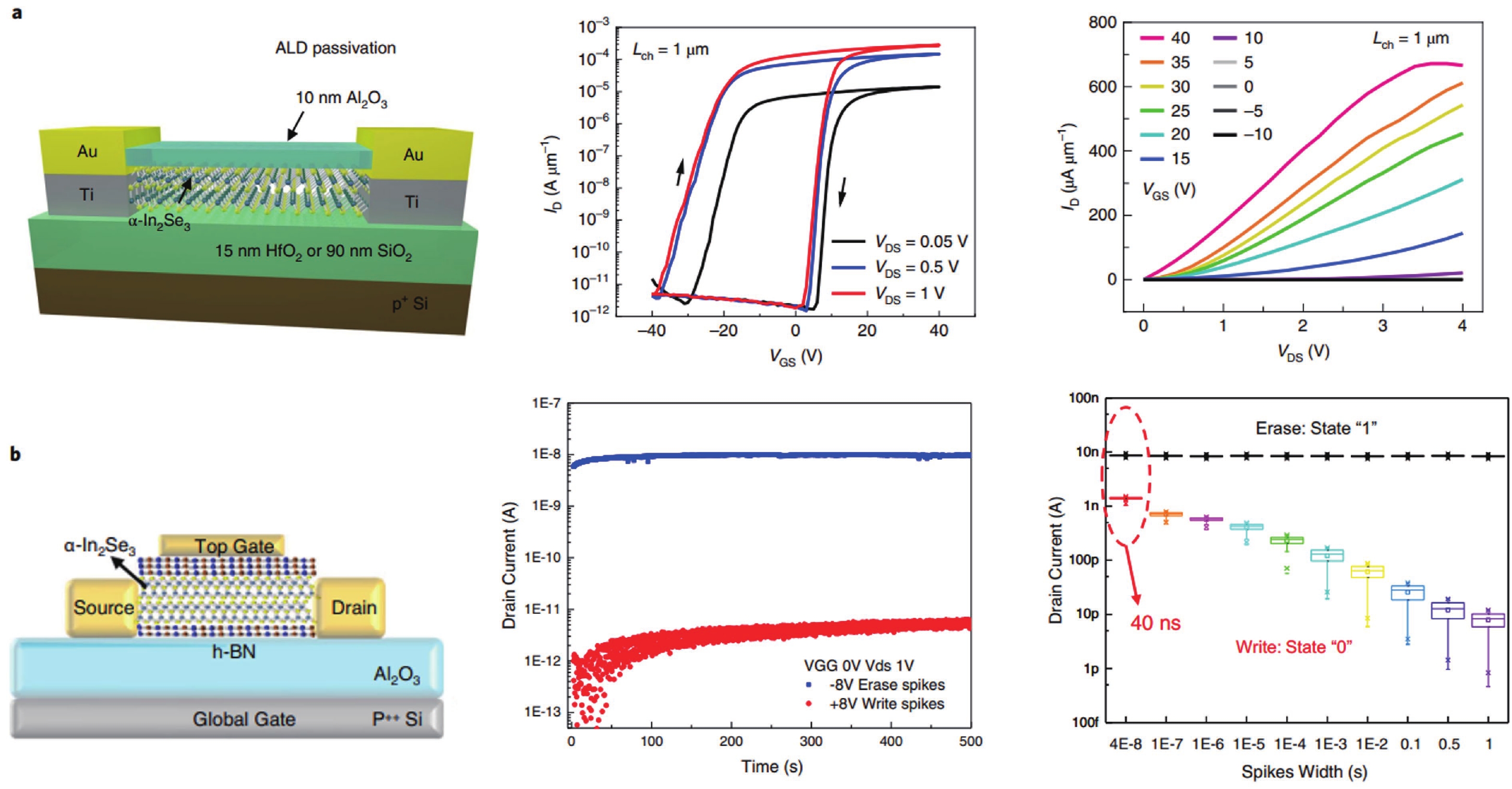
Fig. 2.  (Color online) (a) Schematic structure of α-In2Se3 FeS-FET and switching characteristics of α-In2Se3 FeS-FET (reproduced with permission from Ref. [3], Copyright © 2019, Mengwei Si et al.). (b) Schematic structure of α-In2Se3 FeCTs and switching characteristics of α-In2Se3 FeCTs (reproduced with permission from Ref. [19], Copyright © 2021, Shuiyuan Wang et al.).

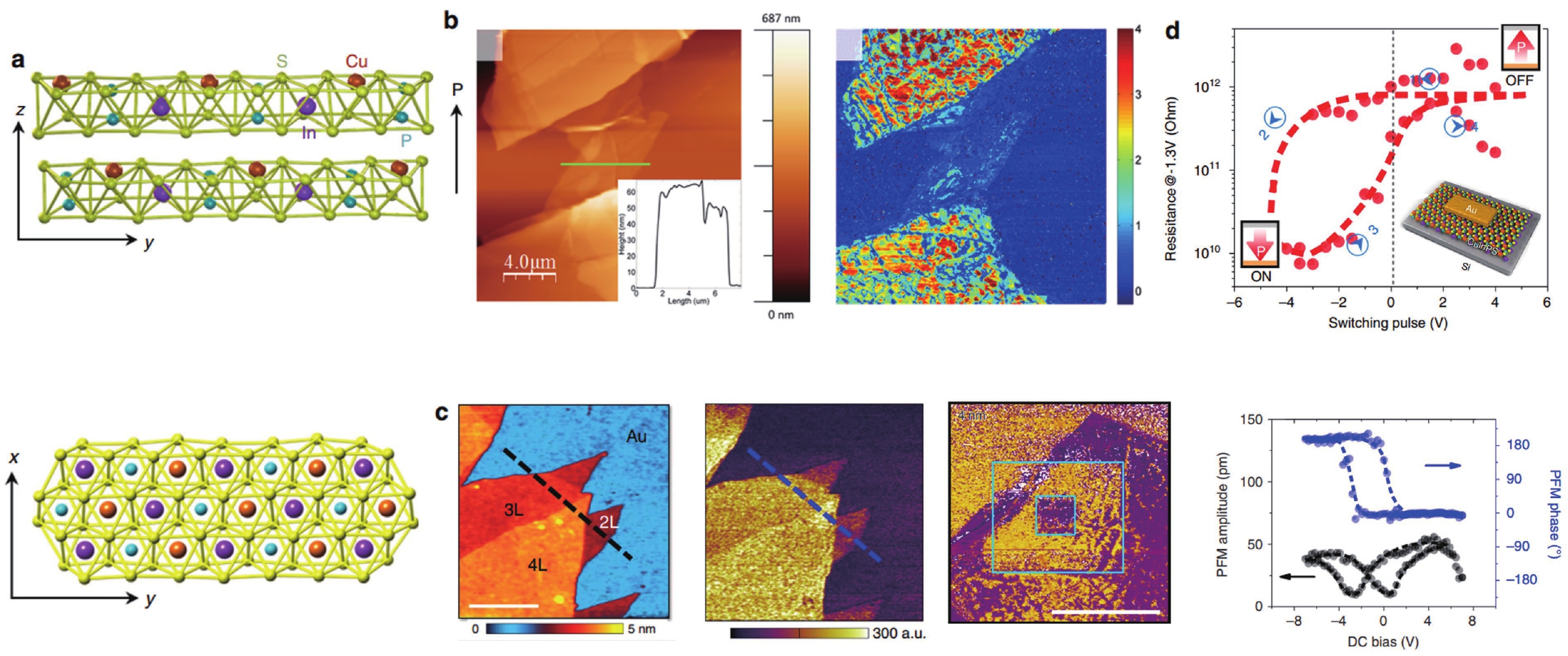
Fig. 3.  (Color online) (a) Schematic crystal structure of CuInP2S6. (b) AFM images and BEPFM images of CuInP2S6 flake (reproduced with permission from Ref. [51], Copyright © 2015, American Chemical Society). (c) AFM images and PFM images of CuInP2S6 flake. (d) Electric characterization of the vdW CuInP2S6/Si diode (Inset: schematic structure of ferroelectric diode based on CuInP2S6 heterostructure). (a), (c) and (d) Reproduced with permission from Ref. [52], Copyright © 2016, Fucai Liu et al.

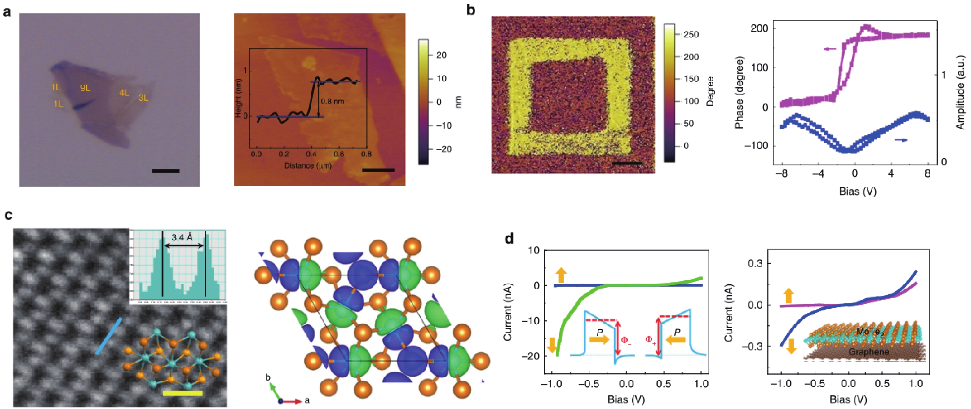
Fig. 4.  (Color online) (a) Optical microscopy and AFM images of d1T-MoTe2. (b) PFM phase hysteretic and butterfly loops of monolayer d1T-MoTe2. (c) Schematic atomic structure of d1T-MoTe2. (d) Electric characterization and structure of the FTJ device d1T-MoTe2. (a-d) Reproduced with permission from Ref. [44], Copyright © 2019, Shuoguo Yuan et al.

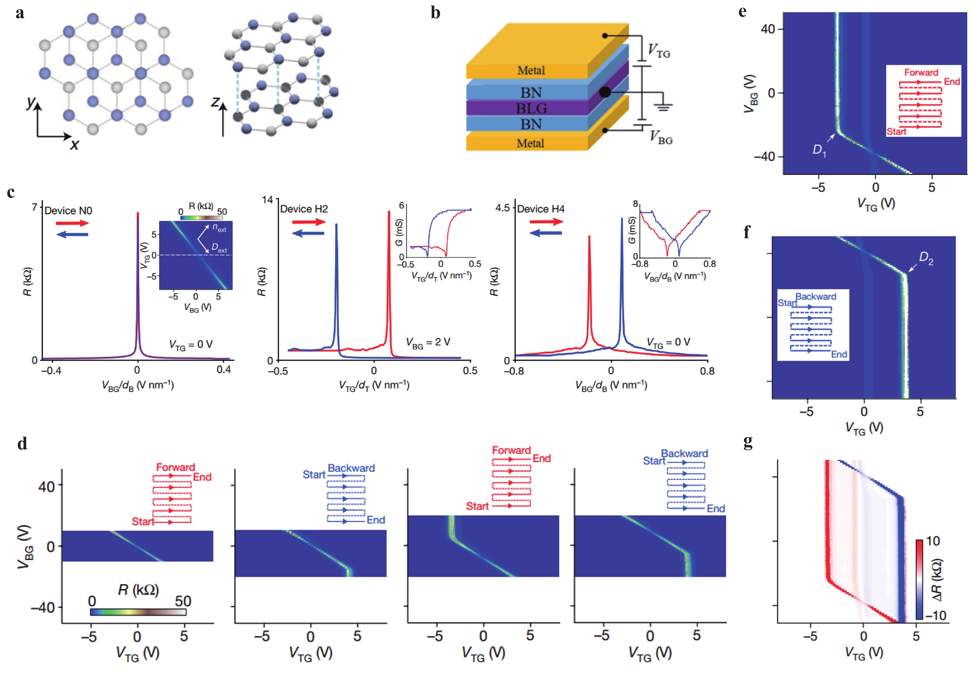
Fig. 5.  (Color online) (a) Schematic crystal structure of Bernal-stacked bilayer graphene (reproduced with permission from Ref. [91], © Springer Nature 2022). (b) Schematic of dual-gate devices N0, H2 and H4. (c) Four-probe resistance for devices N0, H2 and H4. (d) Hysteretic transport behavior for device H4. (Inset: ‘zigzag’ patterns illustrate how data are obtained.) (e) and (f) Forward and backward scan for VBG sweep between –50 and 50 V. (g) The difference between measured in (e) and (f). (b-g) Reproduced with permission from Ref. [74], © Zheng Z et al. 2020.

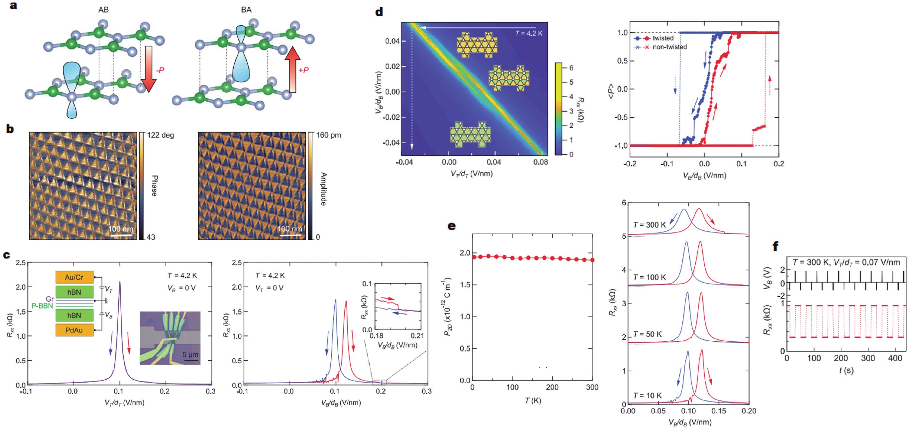
Fig. 6.  (Color online) (a) Schematic crystal structure of AB-stacked and BA-stacked BN. (b) PFM phase and amplitude images of twisted bilayer BN, respectively. (c) Resistance Rxx of graphene for the device as a function of the top gate and bottom gate, respectively (Inset: dual-gate P-BBN device structure). (d) Ferroelectric switching in twisted bilayer BN. (e) Temperature dependence of polarization and graphene resistance Rxx, respectively. (f) Room-temperature operation of a ferroelectric field-effect transistor. (a-f) Reproduced with permission from Ref. [75], © 2021 American Association for the Advancement of Science.

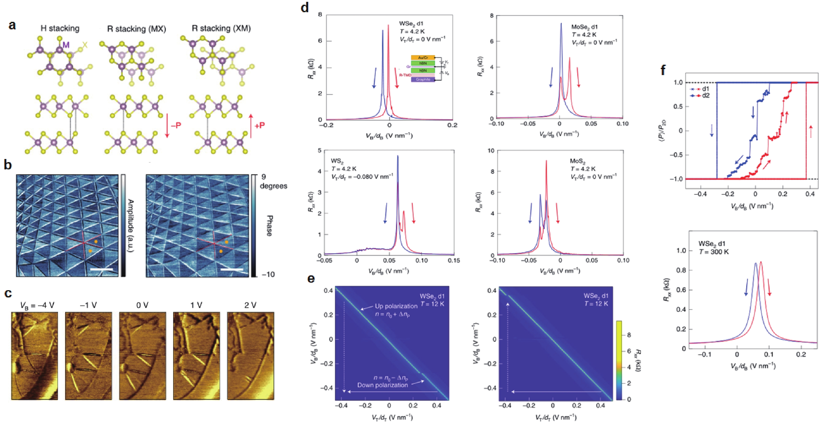
Fig. 7.  (Color online) (a) Schematic crystal structure of H-stacked and R-stacked (MX and XM) TMDs, respectively. (b) PFM phase and amplitude images of MoSe2, respectively. (c) Schematic illustration of lateral PFM measurement on MoSe2. (d) Resistance Rxx of graphene for TMDs device as a function of the top gate and bottom gate, respectively (Inset: dual-gate R-stacked TMDs device structure). (e) Ferroelectric switching in small-angel twisted bilayer WSe2 d1 device. (f) Schematic of polarization switching in WSe2 d1 and d2 device and temperature dependence of graphene resistance Rxx, respectively. (a-f) Reproduced with permission from Ref. [76], © 2021 Springer Nature 2022.

Table 1.   Proved 2D ferroelectric materials.

MaterialTc (K)PolarizationRef.
d1T-MoTe2
In2Se3
α-In2Se3
β’-In2Se3
2H α-In2Se3
CuInP2S6
SnTe
WTe2
BA2PbCl4
RT
700
RT
473
RT
315
270
350
453
Out-of-plane
Out-of-plane
In-plane/Out-of-plane
In-plane
In-plane/Out-of-plane
Out-of-plane
In-plane
Out-of-plane
In-plane
[44]
[47]
[45, 46, 48]
[49]
[50]
[51, 52]
[53]
[54]
[55]
RT: room temperature.
DownLoad: CSV

Table 2.   Twisted 2D ferroelectricity.

MaterialTcAngleLayersRef.
Bernal-stacked bilayer graphene/BN
BN
MoSe2
MoS2
WSe2
WS2

>RT
>RT
>RT
>RT
>RT
30°/0°
0.6°/0°
0.25°/0°
0.25°/0°
0.25°/0°
0.25°/0°
Four-layers
Bilayer
Bilayer
Bilayer
Bilayer
Bilayer
[74]
[75]
[76]
[76]
[76]
[76]
RT: room temperature.
DownLoad: CSV
[1]
Chai X J, Jiang J, Zhang Q H, et al. Nonvolatile ferroelectric field-effect transistors. Nat Commun, 2020, 11, 2811 doi: 10.1038/s41467-020-16623-9
[2]
Naber R C G, Tanase C, Blom P W M, et al. High-performance solution-processed polymer ferroelectric field-effect transistors. Nature Mater, 2005, 4, 243 doi: 10.1038/nmat1329
[3]
Si M W, Saha A K, Gao S J, et al. A ferroelectric semiconductor field-effect transistor. Nat Electron, 2019, 2, 580 doi: 10.1038/s41928-019-0338-7
[4]
Si M W, Liao P Y, Qiu G, et al. Ferroelectric field-effect transistors based on MoS2 and CuInP2S6 two-dimensional van der waals heterostructure. ACS Nano, 2018, 12, 6700 doi: 10.1021/acsnano.8b01810
[5]
Wan S Y, Li Y, Li W, et al. Nonvolatile ferroelectric memory effect in ultrathin α-In2Se3. Adv Funct Mater, 2019, 29, 1808606 doi: 10.1002/adfm.201808606
[6]
Luo Z D, Yang M M, Liu Y, et al. Emerging opportunities for 2D semiconductor/ferroelectric transistor-structure devices. Adv Mater, 2021, 33, 2005620 doi: 10.1002/adma.202005620
[7]
Wu G, Tian B, Liu L, et al. Programmable transition metal dichalcogenide homojunctions controlled by nonvolatile ferroelectric domains. Nat Electron, 2020, 3, 43 doi: 10.1038/s41928-019-0350-y
[8]
Luo Z D, Xia X, Yang M M, et al. Artificial optoelectronic synapses based on ferroelectric field-effect enabled 2D transition metal dichalcogenide memristive transistors. ACS Nano, 2020, 14, 746 doi: 10.1021/acsnano.9b07687
[9]
Lv L, Zhuge F W, Xie F J, et al. Reconfigurable two-dimensional optoelectronic devices enabled by local ferroelectric polarization. Nat Commun, 2019, 10, 3331 doi: 10.1038/s41467-019-11328-0
[10]
Li T, Sharma P, Lipatov A, et al. Polarization-mediated modulation of electronic and transport properties of hybrid MoS2-BaTiO3-SrRuO3 tunnel junctions. Nano Lett, 2017, 17, 922 doi: 10.1021/acs.nanolett.6b04247
[11]
Wang X, Wang P, Wang J, et al. Ultrasensitive and broadband MoS2 photodetector driven by ferroelectrics. Adv Mater, 2015, 27, 6575 doi: 10.1002/adma.201503340
[12]
Lipatov A, Sharma P, Gruverman A, et al. Optoelectrical molybdenum disulfide (MoS2)—Ferroelectric memories. ACS Nano, 2015, 9, 8089 doi: 10.1021/acsnano.5b02078
[13]
Lee H S, Min S W, Park M K, et al. MoS2 Nanosheets for top-gate nonvolatile memory transistor channel. Small, 2012, 8, 3111 doi: 10.1002/smll.201200752
[14]
Scott J F, Paz de Araujo C A. Ferroelectric memories. Science, 1989, 246, 1400 doi: 10.1126/science.246.4936.1400
[15]
Jiang A Q, Wang C, Jin K J, et al. A resistive memory in semiconducting BiFeO3 thin-film capacitors. Adv Mater, 2011, 23, 1277 doi: 10.1002/adma.201004317
[16]
Ishiwara H. Ferroelectric random access memories. J Nanosci Nanotechnol, 2012, 12, 7619 doi: 10.1166/jnn.2012.6651
[17]
Mikolajick T, Slesazeck S, Park M H, et al. Ferroelectric hafnium oxide for ferroelectric random-access memories and ferroelectric field-effect transistors. MRS Bull, 2018, 43, 340 doi: 10.1557/mrs.2018.92
[18]
Hyun S D, Park H W, Park M H, et al. Field-induced ferroelectric Hf1– xZr xO2 thin films for high-k dynamic random access memory. Adv Electron Mater, 2020, 6, 2000631 doi: 10.1002/aelm.202000631
[19]
Wang S, Liu L, Gan L, et al. Two-dimensional ferroelectric channel transistors integrating ultra-fast memory and neural computing. Nat Commun, 2021, 12, 1 doi: 10.1038/s41467-020-20314-w
[20]
Dai M, Li K, Wang F, et al. Intrinsic dipole coupling in 2D van der Waals ferroelectrics for gate-controlled switchable rectifier. Adv Electron Mater, 2020, 6, 1900975 doi: 10.1002/aelm.201900975
[21]
Wan S Y, Li Y, Li W, et al. Room-temperature ferroelectricity and a switchable diode effect in two-dimensional α-In2Se3 thin layers. Nanoscale, 2018, 10, 14885 doi: 10.1039/C8NR04422H
[22]
Poh S M, Tan S J R, Wang H, et al. Molecular-beam epitaxy of two-dimensional In2Se3 and its giant electroresistance switching in ferroresistive memory junction. Nano Lett, 2018, 18, 6340 doi: 10.1021/acs.nanolett.8b02688
[23]
Yoon J, Hong S, Song Y W, et al. Understanding tunneling electroresistance effect through potential profile in Pt/Hf0.5Zr0.5O2/TiN ferroelectric tunnel junction memory. Appl Phys Lett, 2019, 115, 153502 doi: 10.1063/1.5119948
[24]
Goh Y, Jeon S. Enhanced tunneling electroresistance effects in HfZrO-based ferroelectric tunnel junctions by high-pressure nitrogen annealing. Appl Phys Lett, 2018, 113, 052905 doi: 10.1063/1.5040031
[25]
Ambriz-Vargas F, Kolhatkar G, Broyer M, et al. A complementary metal oxide semiconductor process-compatible ferroelectric tunnel junction. ACS Appl Mater Interfaces, 2017, 9, 13262 doi: 10.1021/acsami.6b16173
[26]
Park J Y, Yang K, Lee D H, et al. A perspective on semiconductor devices based on fluorite-structured ferroelectrics from the materials–device integration perspective. J Appl Phys, 2020, 128, 240904 doi: 10.1063/5.0035542
[27]
Xi Z, Ruan J, Li C, et al. Giant tunnelling electroresistance in metal/ferroelectric/semiconductor tunnel junctions by engineering the Schottky barrier. Nat Commun, 2017, 8, 1 doi: 10.1038/s41467-016-0009-6
[28]
Xue F, He X, Liu W, et al. Optoelectronic ferroelectric domain‐wall memories made from a single Van Der Waals ferroelectric. Adv Funct Mater, 2020, 30, 2004206 doi: 10.1002/adfm.202004206
[29]
Xu K, Jiang W, Gao X S, et al. Optical control of ferroelectric switching and multifunctional devices based on van der Waals ferroelectric semiconductors. Nanoscale, 2020, 12, 23488 doi: 10.1039/D0NR06872A
[30]
Wang L, Wang X, Zhang Y, et al. Exploring ferroelectric switching in α-In2Se3 for neuromorphic computing. Adv Funct Mater, 2020, 30, 2004609 doi: 10.1002/adfm.202004609
[31]
Zhang Y S, Wang L, Chen H, et al. Analog and digital mode α-In2Se3 memristive devices for neuromorphic and memory applications. Adv Electron Mater, 2021, 7, 2100609 doi: 10.1002/aelm.202100609
[32]
Kwon K C, Zhang Y S, Wang L, et al. In-plane ferroelectric tin monosulfide and its application in a ferroelectric analog synaptic device. ACS Nano, 2020, 14, 7628 doi: 10.1021/acsnano.0c03869
[33]
Bian J H, Cao Z Y, Zhou P. Neuromorphic computing: Devices, hardware, and system application facilitated by two-dimensional materials. Appl Phys Rev, 2021, 8, 041313 doi: 10.1063/5.0067352
[34]
Dai M, Wang Z, Wang F, et al. Two-dimensional van der Waals materials with aligned in-plane polarization and large piezoelectric effect for self-powered piezoelectric sensors. Nano Lett, 2019, 19, 5410 doi: 10.1021/acs.nanolett.9b01907
[35]
Kim H J, Schanze K. Introducing ACS applied electronic materials. ACS Appl Electron Mater, 2019, 1, 1 doi: 10.1021/acsaelm.8b00087
[36]
Xue F, Zhang J, Hu W, et al. Multidirection piezoelectricity in mono- and multilayered hexagonal α-In2Se3. ACS Nano, 2018, 12, 4976 doi: 10.1021/acsnano.8b02152
[37]
Scott J F. Applications of modern ferroelectrics. Science, 2007, 315, 954 doi: 10.1126/science.1129564
[38]
Prateek, Thakur V K, Gupta R K. Recent progress on ferroelectric polymer-based nanocomposites for high energy density capacitors: Synthesis, dielectric properties, and future aspects. Chem Rev, 2016, 116, 4260 doi: 10.1021/acs.chemrev.5b00495
[39]
Valasek J. Piezo-electric and allied phenomena in rochelle salt. Phys Rev, 1921, 17, 475 doi: 10.1103/PhysRev.17.475
[40]
Junquera J, Ghosez P. Critical thickness for ferroelectricity in perovskite ultrathin films. Nature, 2003, 422, 506 doi: 10.1038/nature01501
[41]
Fong D D, Stephenson G B, Streiffer S K, et al. Ferroelectricity in ultrathin perovskite films. Science, 2004, 304, 1650 doi: 10.1126/science.1098252
[42]
Novoselov K S, Geim A K, Morozov S V, et al. Electric field effect in atomically thin carbon films. Science, 2004, 306, 666 doi: 10.1126/science.1102896
[43]
Lee D, Lu H, Gu Y, et al. Emergence of room-temperature ferroelectricity at reduced dimensions. Science, 2015, 349, 1314 doi: 10.1126/science.aaa6442
[44]
Yuan S G, Luo X, Chan H L, et al. Room-temperature ferroelectricity in MoTe2 down to the atomic monolayer limit. Nat Commun, 2019, 10, 1775 doi: 10.1038/s41467-019-09669-x
[45]
Zhou Y, Wu D, Zhu Y H, et al. Out-of-plane piezoelectricity and ferroelectricity in layered α-In2Se3 nanoflakes. Nano Lett, 2017, 17, 5508 doi: 10.1021/acs.nanolett.7b02198
[46]
Cui C, Hu W J, Yan X, et al. Intercorrelated in-plane and out-of-plane ferroelectricity in ultrathin two-dimensional layered semiconductor In2Se3. Nano Lett, 2018, 18, 1253 doi: 10.1021/acs.nanolett.7b04852
[47]
Xiao J, Zhu H, Wang Y, et al. Intrinsic two-dimensional ferroelectricity with dipole locking. Phys Rev Lett, 2018, 120, 227601 doi: 10.1103/PhysRevLett.120.227601
[48]
Io W F, Yuan S G, Pang S Y, et al. Temperature- and thickness-dependence of robust out-of-plane ferroelectricity in CVD grown ultrathin van der Waals α-In2Se3 layers. Nano Res, 2020, 13, 1897 doi: 10.1007/s12274-020-2640-0
[49]
Zheng C, Yu L, Zhu L, et al. Room temperature in-plane ferroelectricity in van der Waals In2Se3. Sci Adv, 2018, 4, eaar7720 doi: 10.1126/sciadv.aar7720
[50]
Lv B, Yan Z, Xue W, et al. Layer-dependent ferroelectricity in 2H-stacked few-layer α-In2Se3. Mater Horiz, 2021, 8, 1472 doi: 10.1039/D0MH01863E
[51]
Belianinov A, He Q, Dziaugys A, et al. CuInP2S6 room temperature layered ferroelectric. Nano Lett, 2015, 15, 3808 doi: 10.1021/acs.nanolett.5b00491
[52]
Liu F C, You L, Seyler K L, et al. Room-temperature ferroelectricity in CuInP2S6 ultrathin flakes. Nat Commun, 2016, 7, 12357 doi: 10.1038/ncomms12357
[53]
Chang K, Liu J, Lin H, et al. Discovery of robust in-plane ferroelectricity in atomic-thick SnTe. Science, 2016, 353, 274 doi: 10.1126/science.aad8609
[54]
Fei Z, Zhao W, Palomaki T A, et al. Ferroelectric switching of a two-dimensional metal. Nature, 2018, 560, 336 doi: 10.1038/s41586-018-0336-3
[55]
You L, Liu F C, Li H S, et al. In-plane ferroelectricity in thin flakes of van der waals hybrid perovskite. Adv Mater, 2018, 30, 1803249 doi: 10.1002/adma.201803249
[56]
Geim A K, Grigorieva I V. Van der Waals heterostructures. Nature, 2013, 499, 419 doi: 10.1038/nature12385
[57]
Suárez Morell E, Correa J D, Vargas P, et al. Flat bands in slightly twisted bilayer graphene: Tight-binding calculations. Phys Rev B, 2010, 82, 121407 doi: 10.1103/PhysRevB.82.121407
[58]
Yankowitz M, Chen S, Polshyn H, et al. Tuning superconductivity in twisted bilayer graphene. Science, 2019, 363, 1059 doi: 10.1126/science.aav1910
[59]
Wang L, Shih E M, Ghiotto A, et al. Correlated electronic phases in twisted bilayer transition metal dichalcogenides. Nat Mater, 2020, 19, 861 doi: 10.1038/s41563-020-0708-6
[60]
Tang Y H, Li L Z, Li T X, et al. Simulation of Hubbard model physics in WSe2/WS2 moiré superlattices. Nature, 2020, 579, 353 doi: 10.1038/s41586-020-2085-3
[61]
Shen C, Chu Y, Wu Q, et al. Correlated states in twisted double bilayer graphene. Nat Phys, 2020, 16, 520 doi: 10.1038/s41567-020-0825-9
[62]
Sharpe A L, Fox E J, Barnard A W, et al. Emergent ferromagnetism near three-quarters filling in twisted bilayer graphene. Science, 2019, 365, 605 doi: 10.1126/science.aaw3780
[63]
Serlin M, Tschirhart C L, Polshyn H, et al. Intrinsic quantized anomalous Hall effect in a moiré heterostructure. Science, 2020, 367, 900 doi: 10.1126/science.aay5533
[64]
Regan E C, Wang D, Jin C, et al. Mott and generalized Wigner crystal states in WSe2/WS2 moiré superlattices. Nature, 2020, 579, 359 doi: 10.1038/s41586-020-2092-4
[65]
Liu X, Hao Z, Khalaf E, et al. Tunable spin-polarized correlated states in twisted double bilayer graphene. Nature, 2020, 583, 221 doi: 10.1038/s41586-020-2458-7
[66]
Li G H, Luican A, Lopes dos Santos J M B, et al. Observation of Van Hove singularities in twisted graphene layers. Nat Phys, 2010, 6, 109 doi: 10.1038/nphys1463
[67]
Chen G R, Sharpe A L, Fox E J, et al. Tunable correlated Chern insulator and ferromagnetism in a moiré superlattice. Nature, 2020, 579, 56 doi: 10.1038/s41586-020-2049-7
[68]
Chen G R, Jiang L L, Wu S, et al. Evidence of a gate-tunable Mott insulator in a trilayer graphene moiré superlattice. Nat Phys, 2019, 15, 237 doi: 10.1038/s41567-018-0387-2
[69]
Cao Y, Rodan-Legrain D, Rubies-Bigorda O, et al. Tunable correlated states and spin-polarized phases in twisted bilayer-bilayer graphene. Nature, 2020, 583, 215 doi: 10.1038/s41586-020-2260-6
[70]
Cao Y, Fatemi V, Fang S A, et al. Unconventional superconductivity in magic-angle graphene superlattices. Nature, 2018, 556, 43 doi: 10.1038/nature26160
[71]
Cao Y, Fatemi V, Demir A, et al. Correlated insulator behaviour at half-filling in magic-angle graphene superlattices. Nature, 2018, 556, 80 doi: 10.1038/nature26154
[72]
Burg G W, Zhu J H, Taniguchi T, et al. Correlated insulating states in twisted double bilayer graphene. Phys Rev Lett, 2019, 123, 197702 doi: 10.1103/PhysRevLett.123.197702
[73]
Bistritzer R, MacDonald A H. Moiré bands in twisted double-layer graphene. PNAS, 2011, 108, 12233 doi: 10.1073/pnas.1108174108
[74]
Zheng Z R, Ma Q, Bi Z, et al. Unconventional ferroelectricity in moiré heterostructures. Nature, 2020, 588, 71 doi: 10.1038/s41586-020-2970-9
[75]
Yasuda K, Wang X, Watanabe K, et al. Stacking-engineered ferroelectricity in bilayer boron nitride. Science, 2021, 372, 1458 doi: 10.1126/science.abd3230
[76]
Wang X, Yasuda K, Zhang Y, et al. Interfacial ferroelectricity in rhombohedral-stacked bilayer transition metal dichalcogenides. Nat Nanotechnol, 2022, 17, 367 doi: 10.1038/s41565-021-01059-z
[77]
Ding W J, Zhu J B, Wang Z, et al. Prediction of intrinsic two-dimensional ferroelectrics in In2Se3 and other III2-VI3 van der Waals materials. Nat Commun, 2017, 8, 14956 doi: 10.1038/ncomms14956
[78]
Ishiwara H. Current status and prospects of FET-type ferroelectric memories. International Electron Devices Meeting, 2001, 1, 725 doi: 10.1109/IEDM.2001.979615
[79]
Ma T P, Han J P. Why is nonvolatile ferroelectric memory field-effect transistor still elusive. IEEE Electron Device Lett, 2002, 23, 386 doi: 10.1109/LED.2002.1015207
[80]
Yurchuk E, Muller J, Muller S, et al. Charge-trapping phenomena in HfO2-based FeFET-type nonvolatile memories. IEEE Trans Electron Devices, 2016, 63, 3501 doi: 10.1109/TED.2016.2588439
[81]
Simon A, Ravez J, Maisonneuve V, et al. Paraelectric-ferroelectric transition in the lamellar thiophosphate CuInP2S6. Chem Mater, 1994, 6, 1575 doi: 10.1021/cm00045a016
[82]
Maisonneuve V, Reau J M, Dong M, et al. Ionic conductivity in ferroic CuInP2S6 and CuCrP2S6. Ferroelectrics, 1997, 196, 257 doi: 10.1080/00150199708224175
[83]
Kim H J, Kang S H, Hamada I, et al. Origins of the structural phase transitions in MoTe2 and WTe2. Phys Rev B, 2017, 95, 180101 doi: 10.1103/PhysRevB.95.180101
[84]
Keum D H, Cho S, Kim J H, et al. Bandgap opening in few-layered monoclinic MoTe2. Nat Phys, 2015, 11, 482 doi: 10.1038/nphys3314
[85]
Qian X F, Liu J W, Fu L, et al. Quantum spin Hall effect in two-dimensional transition metal dichalcogenides. Science, 2014, 346, 1344 doi: 10.1126/science.1256815
[86]
Eda G, Fujita T, Yamaguchi H, et al. Coherent atomic and electronic heterostructures of single-layer MoS2. ACS Nano, 2012, 6, 7311 doi: 10.1021/nn302422x
[87]
Bruyer E, Di Sante D, Barone P, et al. Possibility of combining ferroelectricity and Rashba-like spin splitting in monolayers of the 1 T-type transition-metal dichalcogenides MX2 (M = Mo, W; X = S, Se, Te). Phys Rev B, 2016, 94, 195402 doi: 10.1103/PhysRevB.94.195402
[88]
Shirodkar S N, Waghmare U V. Emergence of ferroelectricity at a metal-semiconductor transition in a 1T monolayer of MoS2. Phys Rev Lett, 2014, 112, 157601 doi: 10.1103/PhysRevLett.112.157601
[89]
Yang Q, Wu M H, Li J. Origin of two-dimensional vertical ferroelectricity in WTe2 bilayer and multilayer. J Phys Chem Lett, 2018, 9, 7160 doi: 10.1021/acs.jpclett.8b03654
[90]
Castro Neto A H, Guinea F, Peres N M R, et al. The electronic properties of graphene. Rev Mod Phys, 2009, 81, 109 doi: 10.1103/RevModPhys.81.109
[91]
de la Barrera S C, Aronson S, Zheng Z R, et al. Cascade of isospin phase transitions in Bernal-stacked bilayer graphene at zero magnetic field. Nat Phys, 2022, 18, 771 doi: 10.1038/s41567-022-01616-w
[92]
Constantinescu G, Kuc A, Heine T. Stacking in bulk and bilayer hexagonal boron nitride. Phys Rev Lett, 2013, 111, 036104 doi: 10.1103/PhysRevLett.111.036104
[93]
Park H J, Cha J, Choi M, et al. One-dimensional hexagonal boron nitride conducting channel. Sci Adv, 2020, 6, eaay4958 doi: 10.1126/sciadv.aay4958
[94]
Li L, Wu M H. Binary compound bilayer and multilayer with vertical polarizations: Two-dimensional ferroelectrics, multiferroics, and nanogenerators. ACS Nano, 2017, 11, 6382 doi: 10.1021/acsnano.7b02756
[95]
Towle L C, Oberbeck V, Brown B E, et al. Molybdenum diselenide: Rhombohedral high pressure-high temperature polymorph. Science, 1966, 154, 895 doi: 10.1126/science.154.3751.895
[96]
Weston A, Zou Y, Enaldiev V, et al. Atomic reconstruction in twisted bilayers of transition metal dichalcogenides. Nat Nanotechnol, 2020, 15, 592 doi: 10.1038/s41565-020-0682-9
[97]
Cui C J, Xue F, Hu W J, et al. Two-dimensional materials with piezoelectric and ferroelectric functionalities. npj 2D Mater Appl, 2018, 2, 18 doi: 10.1038/s41699-018-0063-5
  • Search

    Advanced Search >>

    GET CITATION

    shu

    Export: BibTex EndNote

    Article Metrics

    Article views: 1780 Times PDF downloads: 296 Times Cited by: 0 Times

    History

    Received: 21 November 2022 Revised: 24 December 2022 Online: Accepted Manuscript: 30 December 2022Uncorrected proof: 30 December 2022Published: 14 January 2023

    Catalog

      Email This Article

      User name:
      Email:*请输入正确邮箱
      Code:*验证码错误
      Xinhao Zhang, Bo Peng. The twisted two-dimensional ferroelectrics[J]. Journal of Semiconductors, 2023, 44(1): 011002. doi: 10.1088/1674-4926/44/1/011002 X H Zhang, B Peng. The twisted two-dimensional ferroelectrics[J]. J. Semicond, 2023, 44(1): 011002. doi: 10.1088/1674-4926/44/1/011002Export: BibTex EndNote
      Citation:
      Xinhao Zhang, Bo Peng. The twisted two-dimensional ferroelectrics[J]. Journal of Semiconductors, 2023, 44(1): 011002. doi: 10.1088/1674-4926/44/1/011002

      X H Zhang, B Peng. The twisted two-dimensional ferroelectrics[J]. J. Semicond, 2023, 44(1): 011002. doi: 10.1088/1674-4926/44/1/011002
      Export: BibTex EndNote

      The twisted two-dimensional ferroelectrics

      doi: 10.1088/1674-4926/44/1/011002
      More Information
      • Author Bio:

        Xinhao Zhang received his B.E. degree from Yangzhou University in 2020. He is a master's student at the National Engineering Research Center for Electromagnetic Radiation Control Materials, University of Electronic Science and Technology of China. He is currently working on the visible and infrared properties of MXene materials

        Bo Peng Professor, received his B.S. (Honors) from Lanzhou University in 2005, and obtained his doctor of philosophy from Technical Institute of Physics and Chemistry, Chinese Academy of Sciences in 2010. He did his postdoctoral research in Singapore between 2010 and 2015. He is currently the head of the Magneto-optical 2D Materials Group in University of Electronic Science and Technology of China. His researches are focused on the two-dimensional multiferroic materials toward spintronic and in-memory computing devices

      • Corresponding author: bo_peng@uestc.edu.cn
      • Received Date: 2022-11-21
      • Revised Date: 2022-12-24
      • Available Online: 2022-12-30

      Catalog

        /

        DownLoad:  Full-Size Img  PowerPoint
        Return
        Return