REVIEWS

Waveguide-integrated optical modulators with two-dimensional materials

Haitao Chen1, 2, 3, Hongyuan Cao1, Zejie Yu1, Weike Zhao1 and Daoxin Dai1, 4,

+ Author Affiliations

 Corresponding author: Daoxin Dai, dxdai@zju.edu.cn

PDF

Turn off MathJax

Abstract: Waveguide-integrated optical modulators are indispensable for on-chip optical interconnects and optical computing. To cope with the ever-increasing amount of data being generated and consumed, ultrafast waveguide-integrated optical modulators with low energy consumption are highly demanded. In recent years, two-dimensional (2D) materials have attracted a lot of attention and have provided tremendous opportunities for the development of high-performance waveguide-integrated optical modulators because of their extraordinary optoelectronic properties and versatile compatibility. This paper reviews the state-of-the-art waveguide-integrated optical modulators with 2D materials, providing researchers with the developing trends in the field and allowing them to identify existing challenges and promising potential solutions. First, the concept and fundamental mechanisms of optical modulation with 2D materials are summarized. Second, a review of waveguide-integrated optical modulators employing electro-optic, all-optic, and thermo-optic effects is provided. Finally, the challenges and perspectives of waveguide-integrated modulators with 2D materials are discussed.

Key words: optical modulationtwo-dimensional (2D) materialson-chipwaveguide


[1]
Srivastava N, Banerjee K. Interconnect challenges for nanoscale electronic circuits. JOM, 2004, 56, 30 doi: 10.1007/s11837-004-0285-1
[2]
Inniss D, Rubenstein R. Silicon photonics: fueling the next information revolution. Morgan Kaufmann, 2016
[3]
Wang J, Long Y. On-chip silicon photonic signaling and processing: A review. Sci Bull, 2018, 63, 1267 doi: 10.1016/j.scib.2018.05.038
[4]
Thomson D, Zilkie A, Bowers J E, et al. Roadmap on silicon photonics. J Opt, 2016, 18, 073003 doi: 10.1088/2040-8978/18/7/073003
[5]
Guo D F, Hou K, Tang W J, et al. Silicon polarization switch based on symmetric polarization splitter-rotators. J Semicond, 2019, 40, 100401 doi: 10.1088/1674-4926/40/10/100401
[6]
Wang H M, Chai H Y, Lv Z R, et al. Silicon photonic transceivers for application in data centers. J Semicond, 2020, 41, 101301 doi: 10.1088/1674-4926/41/10/101301
[7]
Fu X, Dai D. Ultra-small Si-nanowire-based 400 GHz-spacing 15 × 15 arrayed-waveguide grating router with microbends. Electron Lett, 2011, 47, 266 doi: 10.1049/el.2010.3068
[8]
Bogaerts W, De Heyn P, Van Vaerenbergh T, et al. Silicon microring resonators. Laser Photonics Rev, 2012, 6, 47 doi: 10.1002/lpor.201100017
[9]
Dai D X, Bauters J, Bowers J E. Passive technologies for future large-scale photonic integrated circuits on silicon: Polarization handling, light non-reciprocity and loss reduction. Light Sci Appl, 2012, 1, e1 doi: 10.1038/lsa.2012.1
[10]
Dai D X, Liu L, Gao S M, et al. Polarization management for silicon photonic integrated circuits. Laser Photonics Rev, 2013, 7, 303 doi: 10.1002/lpor.201200023
[11]
Zhou Z P, Yin B, Michel J. On-chip light sources for silicon photonics. Light Sci Appl, 2015, 4, e358 doi: 10.1038/lsa.2015.131
[12]
Wang X, Su Z, Zhou Z. Recent progress of silicon photonics. Scientia Sinica Physica, 2015, 45, 014201 doi: 10.1360/SSPMA2014-00300
[13]
Bogaerts W, Chrostowski L. Silicon photonics circuit design: Methods, tools and challenges. Laser Photonics Rev, 2018, 12, 1700237 doi: 10.1002/lpor.201700237
[14]
Liu S T, Khope A. Latest advances in high-performance light sources and optical amplifiers on silicon. J Semicond, 2021, 42, 041307 doi: 10.1088/1674-4926/42/4/041307
[15]
Reed G T, Mashanovich G, Gardes F Y, et al. Silicon optical modulators. Nature Photon, 2010, 4, 518 doi: 10.1038/nphoton.2010.179
[16]
Liu M, Yin X B, Ulin-Avila E, et al. A graphene-based broadband optical modulator. Nature, 2011, 474, 64 doi: 10.1038/nature10067
[17]
Sun Z P, Martinez A, Wang F. Optical modulators with 2D layered materials. Nature Photon, 2016, 10, 227 doi: 10.1038/nphoton.2016.15
[18]
Dai D X, Li J, Yin Y L. Silicon-plus photonics for light manipulation and photodetection. Proc. SPIE 10812, Semiconductor Lasers and Applications VIII, 2018, 1082 doi: 10.1117/12.2503373
[19]
Wang X X, Liu J F. Emerging technologies in Si active photonics. J Semicond, 2018, 39, 061001 doi: 10.1088/1674-4926/39/6/061001
[20]
Su Y K, Zhang Y, Qiu C Y, et al. Silicon photonic platform for passive waveguide devices: Materials, fabrication, and applications. Adv Mater Technol, 2020, 5, 1901153 doi: 10.1002/admt.201901153
[21]
Marris-Morini D, Vakarin V, Ramirez J M, et al. Germanium-based integrated photonics from near- to mid-infrared applications. Nanophotonics, 2018, 7, 1781 doi: 10.1515/nanoph-2018-0113
[22]
Ramirez J M, Elfaiki H, Verolet T, et al. III-V-on-silicon integration: From hybrid devices to heterogeneous photonic integrated circuits. IEEE J Sel Top Quantum Electron, 2020, 26, 1 doi: 10.1109/JSTQE.2019.2939503
[23]
Semond F. Epitaxial challenges of GaN on silicon. MRS Bull, 2015, 40, 412 doi: 10.1557/mrs.2015.96
[24]
Novoselov K S, Geim A K, Morozov S V, et al. Electric field effect in atomically thin carbon films. Science, 2004, 306, 666 doi: 10.1126/science.1102896
[25]
Geim A K. Graphene: Status and prospects. Science, 2009, 324, 1530 doi: 10.1126/science.1158877
[26]
Schaibley J R, Yu H Y, Clark G, et al. Valleytronics in 2D materials. Nat Rev Mater, 2016, 1, 16055 doi: 10.1038/natrevmats.2016.55
[27]
Manzeli S, Ovchinnikov D, Pasquier D, et al. 2D transition metal dichalcogenides. Nat Rev Mater, 2017, 2, 17033 doi: 10.1038/natrevmats.2017.33
[28]
Chen H, Liu M, Xu L, et al. Valley-selective directional emission from a transition-metal dichalcogenide monolayer mediated by a plasmonic nanoantenna, Beilstein. J. Nanotechnol, 2018, 9, 780 doi: 10.3762/bjnano.9.71
[29]
Jiang T, Yin K, Wang C, et al. Ultrafast fiber lasers mode-locked by two-dimensional materials: review and prospect. Photonics Research, 2020, 8(1), 78 doi: 10.1364/PRJ.8.000078
[30]
Novoselov K S, Geim A K, Morozov S V, et al. Two-dimensional gas of massless Dirac fermions in graphene. Nature, 2005, 438, 197 doi: 10.1038/nature04233
[31]
Xia F N, Wang H, Xiao D, et al. Two-dimensional material nanophotonics. Nat Photonics, 2014, 8, 899 doi: 10.1038/nphoton.2014.271
[32]
Caldwell J D, Aharonovich I, Cassabois G, et al. Photonics with hexagonal boron nitride. Nat Rev Mater, 2019, 4, 552 doi: 10.1038/s41578-019-0124-1
[33]
Luo M M, Fan T J, Zhou Y, et al. 2D black phosphorus–based biomedical applications. Adv Funct Mater, 2019, 29, 1808306 doi: 10.1002/adfm.201808306
[34]
Acun A, Zhang L, Bampoulis P, et al. Germanene: The germanium analogue of graphene. J Phys: Condens Matter, 2015, 27, 443002 doi: 10.1088/0953-8984/27/44/443002
[35]
Youngblood N, Li M. Integration of 2D materials on a silicon photonics platform for optoelectronics applications. Nanophotonics, 2016, 6, 1205 doi: 10.1515/nanoph-2016-0155
[36]
Akinwande D, Huyghebaert C, Wang C H, et al. Graphene and two-dimensional materials for silicon technology. Nature, 2019, 573, 507 doi: 10.1038/s41586-019-1573-9
[37]
Yin Y L, Li J, Xu Y, et al. Silicon-graphene photonic devices. J Semicond, 2018, 39, 061009 doi: 10.1088/1674-4926/39/6/061009
[38]
Dai D X, Li J, Song L J. Silicon-plus photonic devices for on-chip light-manipulation and photodetection. Proc. SPIE 11182, Semiconductor Lasers and Applications IX, 2019, 1118206 doi: 10.1117/12.2538255
[39]
Tang Y H, Mak K F. 2D materials for silicon photonics. Nature Nanotech, 2017, 12, 1121 doi: 10.1038/nnano.2017.230
[40]
Chen H T, Nanz S, Abass A, et al. Enhanced directional emission from monolayer WSe2 integrated onto a multiresonant silicon-based photonic structure. ACS Photonics, 2017, 4, 3031 doi: 10.1021/acsphotonics.7b00550
[41]
Ross J S, Wu S F, Yu H Y, et al. Electrical control of neutral and charged excitons in a monolayer semiconductor. Nat Commun, 2013, 4, 1474 doi: 10.1038/ncomms2498
[42]
Ross J S, Klement P, Jones A M, et al. Electrically tunable excitonic light-emitting diodes based on monolayer WSe2 p–n junctions. Nat Nanotechnol, 2014, 9, 268 doi: 10.1038/nnano.2014.26
[43]
Yang J, Xu R J, Pei J J, et al. Optical tuning of exciton and trion emissions in monolayer phosphorene. Light Sci Appl, 2015, 4, e312 doi: 10.1038/lsa.2015.85
[44]
Ouyang H, Chen H T, Tang Y X, et al. All-optical dynamic tuning of local excitonic emission of monolayer MoS2 by integration with Ge2Sb2Te5. Nanophotonics, 2020, 9, 2351 doi: 10.1515/nanoph-2019-0366
[45]
Mouri S, Miyauchi Y, Matsuda K. Tunable photoluminescence of monolayer MoS2 via chemical doping. Nano Lett, 2013, 13, 5944 doi: 10.1021/nl403036h
[46]
Li Z W, Lv Y W, Ren L W, et al. Efficient strain modulation of 2D materials via polymer encapsulation. Nat Commun, 2020, 11, 1151 doi: 10.1038/s41467-020-15023-3
[47]
Novoselov K S, Mishchenko A, Carvalho A, et al. 2D materials and van der Waals heterostructures. Science, 2016, 353(6298), aac9439 doi: 10.1126/science.aac9439
[48]
Liu Y, Weiss N O, Duan X D, et al. Van der waals heterostructures and devices. Nat Rev Mater, 2016, 1, 16042 doi: 10.1038/natrevmats.2016.42
[49]
Gibertini M, Koperski M, Morpurgo A F, et al. Magnetic 2D materials and heterostructures. Nat Nanotechnol, 2019, 14, 408 doi: 10.1038/s41565-019-0438-6
[50]
Wei K, Jiang T, Xu Z J, et al. Hybrid perovskites: Ultrafast carrier transfer promoted by interlayer coulomb coupling in 2D/3D perovskite heterostructures (laser photonics rev. 12(10)/2018). Laser Photonics Rev, 2018, 12, 1870043 doi: 10.1002/lpor.201870043
[51]
Wei K, Sui Y Z, Xu Z J, et al. Acoustic phonon recycling for photocarrier generation in graphene-WS2 heterostructures. Nat Commun, 2020, 11, 3876 doi: 10.1038/s41467-020-17728-x
[52]
Dalir H, Xia Y, Wang Y, et al. Athermal broadband graphene optical modulator with 35 GHz speed. ACS Photonics, 2016, 3, 1564 doi: 10.1021/acsphotonics.6b00398
[53]
Mohsin M, Schall D, Otto M, et al. Graphene based low insertion loss electro-absorption modulator on SOI waveguide. Opt Express, 2014, 22, 15292 doi: 10.1364/OE.22.015292
[54]
Lu Z L, Zhao W S. Nanoscale electro-optic modulators based on graphene-slot waveguides. J Opt Soc Am B, 2012, 29, 1490 doi: 10.1364/JOSAB.29.001490
[55]
Jiao J Y, Hao R, Zhen Z, et al. Optimization of graphene-based slot waveguides for efficient modulation. IEEE J Sel Top Quantum Electron, 2020, 26, 1 doi: 10.1109/JSTQE.2019.2941469
[56]
Cheng Z, Zhu X L, Galili M, et al. Double-layer graphene on photonic crystal waveguide electro-absorption modulator with 12 GHz bandwidth. Nanophotonics, 2020, 9, 2377 doi: 10.1515/nanoph-2019-0381
[57]
Shi Z, Gan L, Xiao T H, et al. All-optical modulation of a graphene-cladded silicon photonic crystal cavity. ACS Photonics, 2015, 2, 1513 doi: 10.1021/acsphotonics.5b00469
[58]
Ding Y, Guan X, Zhu X, et al. Efficient electro-optic modulation in low-loss graphene-plasmonic slot waveguides. Nanoscale, 2017, 9, 15576 doi: 10.1039/C7NR05994A
[59]
Ono M, Hata M, Tsunekawa M, et al. Ultrafast and energy-efficient all-optical switching with graphene-loaded deep-subwavelength plasmonic waveguides. Nat Photonics, 2020, 14, 37 doi: 10.1038/s41566-019-0547-7
[60]
Phare C T, Lee Y H D, Cardenas J, et al. Graphene electro-optic modulator with 30 GHz bandwidth. Nat Photonics, 2015, 9, 511 doi: 10.1038/nphoton.2015.122
[61]
Gan S, Cheng C T, Zhan Y H, et al. A highly efficient thermo-optic microring modulator assisted by graphene. Nanoscale, 2015, 7, 20249 doi: 10.1039/C5NR05084G
[62]
Xu Z Z, Qiu C Y, Yang Y X, et al. Ultra-compact tunable silicon nanobeam cavity with an energy-efficient graphene micro-heater. Opt Express, 2017, 25, 19479 doi: 10.1364/OE.25.019479
[63]
Jafari Z, Zarifkar A, Miri M, et al. All-optical modulation in a graphene-covered slotted silicon nano-beam cavity. J Light Technol, 2018, 36, 4051 doi: 10.1109/JLT.2018.2858551
[64]
Chai Z, Hu X, Wang F, et al. Ultrafast All-Optical Switching. Adv Opt Mater, 2017, 5(7), 1600665 doi: 10.1002/adom.201600665
[65]
Yao Y H, Cheng Z, Dong J J, et al. Performance of integrated optical switches based on 2D materials and beyond. Front Optoelectron, 2020, 13, 129 doi: 10.1007/s12200-020-1058-3
[66]
Yu S L, Wu X Q, Wang Y P, et al. 2D materials for optical modulation: Challenges and opportunities. Adv Mater, 2017, 29, 1606128 doi: 10.1002/adma.201606128
[67]
Chen H T, Wang C, Ouyang H, et al. All-optical modulation with 2D layered materials: Status and prospects. Nanophotonics, 2020, 9, 2107 doi: 10.1515/nanoph-2019-0493
[68]
You J, Luo Y K, Yang J, et al. Hybrid/integrated silicon photonics based on 2D materials in optical communication nanosystems. Laser Photonics Rev, 2020, 14, 2000239 doi: 10.1002/lpor.202000239
[69]
Gan X, Englund D, Van Thourhout D, et al. 2D materials-enabled optical modulators: From visible to terahertz spectral range. Appl Phys Rev, 2022, 9(2), 021302 doi: 10.1063/5.0078416
[70]
Yang H Y, Wang Y Z, Tiu Z C, et al. All-optical modulation technology based on 2D layered materials. Micromachines, 2022, 13, 92 doi: 10.3390/mi13010092
[71]
Wang G Z, Baker-Murray A A, Blau W J. Saturable absorption in 2D nanomaterials and related photonic devices. Laser Photonics Rev, 2019, 13, 1800282 doi: 10.1002/lpor.201800282
[72]
Li Q, Lu J, Gupta P, et al. Engineering optical absorption in graphene and other 2D materials: Advances and applications. Adv Opt Mater, 2019, 7, 1900595 doi: 10.1002/adom.201900595
[73]
Cheng J L, Sipe J E, Vermeulen N, et al. Nonlinear optics of graphene and other 2D materials in layered structures. J Phys Photonics, 2018, 1, 015002 doi: 10.1088/2515-7647/aaeadb
[74]
Wu K, Wang Y F, Qiu C Y, et al. Thermo-optic all-optical devices based on two-dimensional materials. Photon Res, 2018, 6, C22 doi: 10.1364/PRJ.6.000C22
[75]
Optical modulation. Cambridge University Press, Cambridge, 2016
[76]
Miller D A B. Energy consumption in optical modulators for interconnects. Opt Express, 2012, 20, A293 doi: 10.1364/OE.20.00A293
[77]
Datta I, Chae S H, Bhatt G R, et al. Low-loss composite photonic platform based on 2D semiconductor monolayers. Nat Photonics, 2020, 14, 256 doi: 10.1038/s41566-020-0590-4
[78]
Cheng Z, Cao R, Guo J, et al. Phosphorene-assisted silicon photonic modulator with fast response time. Nanophotonics, 2020, 9, 1973 doi: 10.1515/nanoph-2019-0510
[79]
Lin H T, Song Y, Huang Y Z, et al. Chalcogenide glass-on-graphene photonics. Nature Photon, 2017, 11, 798 doi: 10.1038/s41566-017-0033-z
[80]
Bao X Z, Ou Q D, Xu Z Q, et al. Band structure engineering in 2D materials for optoelectronic applications. Adv Mater Technol, 2018, 3, 1800072 doi: 10.1002/admt.201800072
[81]
Wang F, Zhang Y B, Tian C S, et al. Gate-variable optical transitions in graphene. Science, 2008, 320, 206 doi: 10.1126/science.1152793
[82]
Liu Y P, Tom K, Wang X, et al. Dynamic control of optical response in layered metal chalcogenide nanoplates. Nano Lett, 2016, 16, 488 doi: 10.1021/acs.nanolett.5b04140
[83]
Liu M, Yin X B, Zhang X. Double-layer graphene optical modulator. Nano Lett, 2012, 12, 1482 doi: 10.1021/nl204202k
[84]
Youngblood N, Anugrah Y, Ma R, et al. Multifunctional graphene optical modulator and photodetector integrated on silicon waveguides. Nano Lett, 2014, 14, 2741 doi: 10.1021/nl500712u
[85]
Sorianello V, Midrio M, Contestabile G, et al. Graphene–silicon phase modulators with gigahertz bandwidth. Nat Photonics, 2018, 12, 40 doi: 10.1038/s41566-017-0071-6
[86]
Agarwal H, Terrés B, Orsini L, et al. 2D-3D integration of hexagonal boron nitride and a high-κ dielectric for ultrafast graphene-based electro-absorption modulators. Nat Commun, 2021, 12, 1 doi: 10.1038/s41467-020-20314-w
[87]
Koester S J, Li M. High-speed waveguide-coupled graphene-on-graphene optical modulators. Appl Phys Lett, 2012, 100, 171107. doi: 10.1063/1.4704663
[88]
Hao R, Jin J M. Graphene embedded modulator with extremely small footprint and high modulation efficiency. J Photonics, 2014, 2014, 309350 doi: 10.1155/2014/309350
[89]
Hao R, Ye Z W, Gu Y J, et al. Large modulation capacity in graphene-based slot modulators by enhanced hybrid plasmonic effects. Sci Rep, 2018, 8, 16830 doi: 10.1038/s41598-018-34914-6
[90]
Midrio M, Galli P, Romagnoli M, et al. Graphene-based optical phase modulation of waveguide transverse electric modes. Photon Res, 2014, 2, A34 doi: 10.1364/PRJ.2.000A34
[91]
Qiu C Y, Gao W L, Vajtai R, et al. Efficient modulation of 1.55 μm radiation with gated graphene on a silicon microring resonator. Nano Lett, 2014, 14, 6811 doi: 10.1021/nl502363u
[92]
Ding Y H, Zhu X L, Xiao S S, et al. Effective electro-optical modulation with high extinction ratio by a graphene–silicon microring resonator. Nano Lett, 2015, 15, 4393 doi: 10.1021/acs.nanolett.5b00630
[93]
Luo S Y, Wang Y N, Tong X, et al. Graphene-based optical modulators. Nanoscale Res Lett, 2015, 10, 1 doi: 10.1186/1556-276X-10-1
[94]
Shi Y X, Li J S, Zhang L. Graphene-integrated split-ring resonator terahertz modulator. Opt Quantum Electron, 2017, 49, 350 doi: 10.1007/s11082-017-1198-x
[95]
Xu C, Jin Y C, Yang L Z, et al. Characteristics of electro-refractive modulating based on graphene-oxide-silicon waveguide. Opt Express, 2012, 20, 22398 doi: 10.1364/OE.20.022398
[96]
Yang L Z, Hu T, Hao R, et al. Low-chirp high-extinction-ratio modulator based on graphene–silicon waveguide. Opt Lett, 2013, 38, 2512 doi: 10.1364/OL.38.002512
[97]
Hao R, Du W, Chen H S, et al. Ultra-compact optical modulator by graphene induced electro-refraction effect. Appl Phys Lett, 2013, 103, 061161 doi: 10.1063/1.4818457
[98]
Mohsin M, Neumaier D, Schall D, et al. Experimental verification of electro-refractive phase modulation in graphene. Sci Rep, 2015, 5, 10967 doi: 10.1038/srep10967
[99]
Ye S W, Wang Z S, Tang L F, et al. Electro-absorption optical modulator using dual-graphene-on-graphene configuration. Opt Express, 2014, 22, 26173 doi: 10.1364/OE.22.026173
[100]
Gao Y D, Shiue R J, Gan X T, et al. High-speed electro-optic modulator integrated with graphene-boron nitride heterostructure and photonic crystal nanocavity. Nano Lett, 2015, 15, 2001 doi: 10.1021/nl504860z
[101]
Hu Y T, Pantouvaki M, Van Campenhout J, et al. Broadband 10 Gb/s operation of graphene electro-absorption modulator on silicon. Laser Photonics Rev, 2016, 10, 307 doi: 10.1002/lpor.201500250
[102]
Ye S W, Yuan F, Zou X H, et al. High-speed optical phase modulator based on graphene-silicon waveguide. IEEE J Sel Top Quantum Electron, 2017, 23, 76 doi: 10.1109/JSTQE.2016.2545238
[103]
Yu Z J, Wang Y, Sun B L, et al. Hybrid 2D-material photonics with bound states in the continuum. Adv Optical Mater, 2019, 7, 1901306 doi: 10.1002/adom.201901306
[104]
Luan C, Kong D M, Ding Y H, et al. High-modulation-efficiency graphene-silicon slot-waveguide micro-ring modulator. Conference on Lasers and Electro-Optics, San Jose, 2022 doi: 10.1364/CLEO_AT.2022.JTh6B.8
[105]
Gosciniak J, Tan D T H. Theoretical investigation of graphene-based photonic modulators. Sci Rep, 2013, 3, 1897 doi: 10.1038/srep01897
[106]
Gan X T, Zhao C Y, Wang Y D, et al. Graphene-assisted all-fiber phase shifter and switching. Optica, 2015, 2, 468 doi: 10.1364/OPTICA.2.000468
[107]
Lee E J, Choi S Y, Jeong H, et al. Active control of all-fibre graphene devices with electrical gating. Nat Commun, 2015, 6, 6851 doi: 10.1038/ncomms7851
[108]
Hu Y Z, You J, Tong M Y, et al. Metaphotonic devices: Pump-color selective control of ultrafast all-optical switching dynamics in metaphotonic devices (adv. sci. 14/2020). Adv Sci, 2020, 7, 2070080 doi: 10.1002/advs.202070080
[109]
Bao Q L, Zhang H, Wang Y, et al. Atomic-layer graphene as a saturable absorber for ultrafast pulsed lasers. Adv Funct Mater, 2009, 19, 3077 doi: 10.1002/adfm.200901007
[110]
Sun Z P, Hasan T, Torrisi F, et al. Graphene mode-locked ultrafast laser. ACS Nano, 2010, 4, 803 doi: 10.1021/nn901703e
[111]
Zhang B T, Liu J, Wang C, et al. Recent progress in 2D material-based saturable absorbers for all solid-state pulsed bulk lasers. Laser Photonics Rev, 2020, 14, 1900240 doi: 10.1002/lpor.201900240
[112]
Hendry E, Hale P J, Moger J, et al. Coherent nonlinear optical response of graphene. Phys Rev Lett, 2010, 105, 097401 doi: 10.1103/PhysRevLett.105.097401
[113]
Wang J, Hernandez Y, Lotya M, et al. Broadband nonlinear optical response of graphene dispersions. Adv Mater, 2009, 21, 2430 doi: 10.1002/adma.200803616
[114]
Bao Q L, Zhang H, Wang B, et al. Broadband graphene polarizer. Nat Photonics, 2011, 5, 411 doi: 10.1038/nphoton.2011.102
[115]
Yu L H, Zheng J J, Xu Y, et al. Local and nonlocal optically induced transparency effects in graphene–silicon hybrid nanophotonic integrated circuits. ACS Nano, 2014, 8, 11386 doi: 10.1021/nn504377m
[116]
Ooi K J A, Leong P C, Ang L K, et al. All-optical control on a graphene-on-silicon waveguide modulator. Sci Rep, 2017, 7, 1 doi: 10.1038/s41598-016-0028-x
[117]
Demongodin P, El Dirani H, Lhuillier J, et al. Ultrafast saturable absorption dynamics in hybrid graphene/Si3N4 waveguides. APL Photonics, 2019, 4, 076102 doi: 10.1063/1.5094523
[118]
Wang H, Yang N N, Chang L M, et al. CMOS-compatible all-optical modulator based on the saturable absorption of graphene. Photon Res, 2020, 8, 468 doi: 10.1364/PRJ.380170
[119]
Chen H T, Corboliou V, Solntsev A S, et al. Enhanced second-harmonic generation from two-dimensional MoSe2 on a silicon waveguide. Light Sci Appl, 2017, 6, e17060 doi: 10.1038/lsa.2017.60
[120]
Yang S, Liu D C, Tan Z L, et al. CMOS-compatible WS2-based all-optical modulator. ACS Photonics, 2018, 5, 342 doi: 10.1021/acsphotonics.7b01206
[121]
Klein M, Badada B H, Binder R, et al. 2D semiconductor nonlinear plasmonic modulators. Nat Commun, 2019, 10, 3264 doi: 10.1038/s41467-019-11186-w
[122]
Sun F Y, Xia L P, Nie C B, et al. An all-optical modulator based on a graphene–plasmonic slot waveguide at 1550 nm. Appl Phys Express, 2019, 12, 042009 doi: 10.7567/1882-0786/ab0a89
[123]
Sun F Y, Xia L P, Nie C B, et al. The all-optical modulator in dielectric-loaded waveguide with graphene-silicon heterojunction structure. Nanotechnology, 2018, 29, 135201 doi: 10.1088/1361-6528/aaa8be
[124]
Alaloul M, Khurgin J B. High-performance all-optical modulator based on graphene-HBN heterostructures. IEEE J Sel Top Quantum Electron, 2022, 28, 1 doi: 10.1109/JSTQE.2022.3206066
[125]
Yu S L, Meng C, Chen B G, et al. Graphene decorated microfiber for ultrafast optical modulation. Opt Express, 2015, 23, 10764 doi: 10.1364/OE.23.010764
[126]
Li W, Chen B G, Meng C, et al. Ultrafast all-optical graphene modulator. Nano Lett, 2014, 14, 955 doi: 10.1021/nl404356t
[127]
Sun D, Wu Z K, Divin C, et al. Ultrafast relaxation of excited Dirac fermions in epitaxial graphene using optical differential transmission spectroscopy. Phys Rev Lett, 2008, 101, 157402 doi: 10.1103/PhysRevLett.101.157402
[128]
Dong P, Qian W, Liang H, et al. Thermally tunable silicon racetrack resonators with ultralow tuning power. Opt Express, 2010, 18, 20298 doi: 10.1364/OE.18.020298
[129]
Dong P, Shafiiha R, Liao S R, et al. Wavelength-tunable silicon microring modulator. Opt Express, 2010, 18, 10941 doi: 10.1364/OE.18.010941
[130]
Renteria J, Nika D, Balandin A. Graphene thermal properties: Applications in thermal management and energy storage. Appl Sci, 2014, 4, 525 doi: 10.3390/app4040525
[131]
Kang J M, Kim H, Kim K S, et al. High-performance graphene-based transparent flexible heaters. Nano Lett, 2011, 11, 5154 doi: 10.1021/nl202311v
[132]
Yu L H, Shi Y C, He S L, et al. Tunable silicon micro-disk resonator with flexible graphene-based ultra-thin heaters. Asia Communications and Photonics Conference 2015, 2015, AS3B. 2
[133]
Yu L, He S, Zheng J, et al. Graphene-based transparent nano-heater for thermally-tuning silicon nanophotonic integrated devices. Progress in Electromagnetics Research Symposium, 2014, 1735
[134]
Yu L H, Yin Y L, Shi Y C, et al. Thermally tunable silicon photonic microdisk resonator with transparent graphene nanoheaters. Optica, 2016, 3, 159 doi: 10.1364/OPTICA.3.000159
[135]
Yan S Q, Zhu X L, Frandsen L H, et al. Slow-light-enhanced energy efficiency for graphene microheaters on silicon photonic crystal waveguides. Nat Commun, 2017, 8, 14411 doi: 10.1038/ncomms14411
[136]
Qiu C Y, Yang Y X, Li C, et al. All-optical control of light on a graphene-on-silicon nitride chip using thermo-optic effect. Sci Rep, 2017, 7, 17046 doi: 10.1038/s41598-017-16989-9
[137]
Liu Y J, Wang H D, Wang S, et al. Highly efficient silicon photonic microheater based on black arsenic–phosphorus. Adv Optical Mater, 2020, 8, 1901526 doi: 10.1002/adom.201901526
[138]
Cao H Y, Chen H T, Pan Y, et al. Efficient and fast all-optical modulator with in situ grown MoTe2 nanosheets on silicon. ACS Appl Nano Mater, 2023, 6, 838 doi: 10.1021/acsanm.2c03393
[139]
Yu L H, Dai D X, He S L. Graphene-based transparent flexible heat conductor for thermally tuning nanophotonic integrated devices. Appl Phys Lett, 2014, 105, 251104 doi: 10.1063/1.4905002
[140]
Wei K K, Li D L, Lin Z T, et al. All-optical PtSe2 silicon photonic modulator with ultra-high stability. Photon Res, 2020, 8, 1189 doi: 10.1364/PRJ.392512
[141]
Li Z W, Liu Q, Wang H, et al. Photo-induced thermo-optical refraction switching by a graphene-assisted silicon microring resonator. J Light Technol, 2021, 39, 3471 doi: 10.1109/JLT.2021.3065686
[142]
Guo T, Gao S, Zeng H Y, et al. All-optical control of a single resonance in a graphene-on-silicon nanobeam cavity using thermo-optic effect. J Light Technol, 2021, 39, 4710 doi: 10.1109/JLT.2021.3077559
[143]
Qiu C Y, Zhang C, Zeng H Y, et al. High-performance graphene-on-silicon nitride all-optical switch based on a Mach–Zehnder interferometer. J Light Technol, 2021, 39, 2099 doi: 10.1109/JLT.2020.3045472
[144]
Nakamura S, Sekiya K, Matano S, et al. High-speed and on-chip optical switch based on a graphene microheater. ACS Nano, 2022, 16, 2690 doi: 10.1021/acsnano.1c09526
[145]
Bonaccorso F, Sun Z, Hasan T, et al. Graphene photonics and optoelectronics. Nat Photonics, 2010, 4, 611 doi: 10.1038/nphoton.2010.186
[146]
Gruhler N, Benz C, Jang H, et al. High-quality Si3N4 circuits as a platform for graphene-based nanophotonic devices. Opt Express, 2013, 21, 31678 doi: 10.1364/OE.21.031678
[147]
Gan X T, Shiue R J, Gao Y D, et al. Chip-integrated ultrafast graphene photodetector with high responsivity. Nat Photonics, 2013, 7, 883 doi: 10.1038/nphoton.2013.253
[148]
Li H, Anugrah Y, Koester S J, et al. Optical absorption in graphene integrated on silicon waveguides. Appl Phys Lett, 2012, 101, 111110 doi: 10.1063/1.4752435
[149]
Schall D, Neumaier D, Mohsin M, et al. 50 GBit/s photodetectors based on wafer-scale graphene for integrated silicon photonic communication systems. ACS Photonics, 2014, 1, 781 doi: 10.1021/ph5001605
[150]
Nyakiti L O, Wheeler V D, Garces N Y, et al. Enabling graphene-based technologies: Toward wafer-scale production of epitaxial graphene. MRS Bull, 2012, 37, 1149 doi: 10.1557/mrs.2012.180
[151]
Huang C C, Al-Saab F, Wang Y D, et al. Scalable high-mobility MoS2 thin films fabricated by an atmospheric pressure chemical vapor deposition process at ambient temperature. Nanoscale, 2014, 6, 12792 doi: 10.1039/C4NR04228J
[152]
Zhou L, Xu K, Zubair A, et al. Large-area synthesis of high-quality uniform few-layer MoTe2. J Am Chem Soc, 2015, 137, 11892 doi: 10.1021/jacs.5b07452
[153]
Colombo L, Wallace R M, Ruoff R S. Graphene growth and device integration. Proc IEEE, 2013, 101, 1536 doi: 10.1109/JPROC.2013.2260114
[154]
Lee B, Mordi G, Kim M J, et al. Characteristics of high-k Al2O3 dielectric using ozone-based atomic layer deposition for dual-gated graphene devices. Appl Phys Lett, 2010, 97, 043107 doi: 10.1063/1.3467454
[155]
Williams J R, DiCarlo L, Marcus C M. Quantum Hall effect in a gate-controlled p-n junction of graphene. Science, 2007, 317, 638 doi: 10.1126/science.1144657
[156]
Wang X R, Tabakman S M, Dai H J. Atomic layer deposition of metal oxides on pristine and functionalized graphene. J Am Chem Soc, 2008, 130, 8152 doi: 10.1021/ja8023059
[157]
Yu Z J, Xi X, Ma J W, et al. Photonic integrated circuits with bound states in the continuum. Optica, 2019, 6, 1342 doi: 10.1364/OPTICA.6.001342
[158]
Yu Z J, Tong Y Y, Tsang H K, et al. High-dimensional communication on etchless lithium niobate platform with photonic bound states in the continuum. Nat Commun, 2020, 11, 2602 doi: 10.1038/s41467-020-15358-x
[159]
Barnes W L, Dereux A, Ebbesen T W. Surface plasmon subwavelength optics. Nature, 2003, 424, 824 doi: 10.1038/nature01937
[160]
Bozhevolnyi S I, Volkov V S, Devaux E, et al. Channel plasmon subwavelength waveguide components including interferometers and ring resonators. Nature, 2006, 440, 508 doi: 10.1038/nature04594
[161]
Gramotnev D K, Bozhevolnyi S I. Plasmonics beyond the diffraction limit. Nature Photon, 2010, 4, 83 doi: 10.1038/nphoton.2009.282
[162]
Chen H T, Yang J, Rusak E, et al. Manipulation of photoluminescence of two-dimensional MoSe2 by gold nanoantennas. Sci Rep, 2016, 6, 22296 doi: 10.1038/srep22296
[163]
He W B, Chen H T, Ouyang H, et al. Tunable anisotropic plasmon response of monolayer GeSe nanoribbon arrays. Nanoscale, 2020, 12, 16762 doi: 10.1039/D0NR02047H
[164]
MacDonald K F, Sámson Z L, Stockman M I, et al. Ultrafast active plasmonics. Nat Photonics, 2009, 3, 55 doi: 10.1038/nphoton.2008.249
[165]
Ono M, Taniyama H, Xu H, et al. Deep-subwavelength plasmonic mode converter with large size reduction for Si-wire waveguide. Optica, 2016, 3, 999 doi: 10.1364/OPTICA.3.000999
[166]
Huang B H, Lu W B, Li X B, et al. Waveguide-coupled hybrid plasmonic modulator based on graphene. Appl Opt, 2016, 55, 5598 doi: 10.1364/AO.55.005598
[167]
Gosciniak J, Tan D T H. Graphene-based waveguide integrated dielectric-loaded plasmonic electro-absorption modulators. Nanotechnology, 2013, 24, 185202 doi: 10.1088/0957-4484/24/18/185202
[168]
Kim J T, Chung K H, Choi C G. Thermo-optic mode extinction modulator based on graphene plasmonic waveguide. Opt Express, 2013, 21, 15280 doi: 10.1364/OE.21.015280
[169]
Rezaei M H, Zarifkar A. Graphene-based plasmonic electro-optical SR flip-flop with an ultra-compact footprint. Opt Express, 2020, 28, 25167 doi: 10.1364/OE.398597
[170]
Shirdel M, Ali Mansouri-Birjandi M. A broadband graphene modulator based on plasmonic valley-slot waveguide. Opt Quantum Electron, 2020, 52, 36 doi: 10.1007/s11082-019-2138-8
[171]
Ansell D, Radko I P, Han Z, et al. Hybrid graphene plasmonic waveguide modulators. Nat Commun, 2015, 6, 8846 doi: 10.1038/ncomms9846
[172]
Mounet N, Gibertini M, Schwaller P, et al. Two-dimensional materials from high-throughput computational exfoliation of experimentally known compounds. Nat Nanotechnol, 2018, 13, 246 doi: 10.1038/s41565-017-0035-5
[173]
Staude I, Schilling J. Metamaterial-inspired silicon nanophotonics. Nature Photon, 2017, 11, 274 doi: 10.1038/nphoton.2017.39
[174]
Xu H N, Dai D X, Shi Y C. Ultra-broadband and ultra-compact on-chip silicon polarization beam splitter by using hetero-anisotropic metamaterials. Laser Photonics Rev, 2019, 13, 1800349 doi: 10.1002/lpor.201800349
[175]
Wang Y, Yu J Y, Mao Y F, et al. Stable, high-performance sodium-based plasmonic devices in the near infrared. Nature, 2020, 581, 401 doi: 10.1038/s41586-020-2306-9
[176]
Dai D X, Shi Y C, He S L, et al. Gain enhancement in a hybrid plasmonic nano-waveguide with a low-index or high-index gain medium. Opt Express, 2011, 19, 12925 doi: 10.1364/OE.19.012925
[177]
Liang G Z, Huang H Q, Mohanty A, et al. Robust, efficient, micrometre-scale phase modulators at visible wavelengths. Nat Photonics, 2021, 15, 908 doi: 10.1038/s41566-021-00891-y
[178]
Pan B C, Hu J Y, Huang Y S, et al. Demonstration of high-speed thin-film lithium-niobate-on-insulator optical modulators at the 2-µm wavelength. Opt Express, 2021, 29, 17710 doi: 10.1364/OE.416908
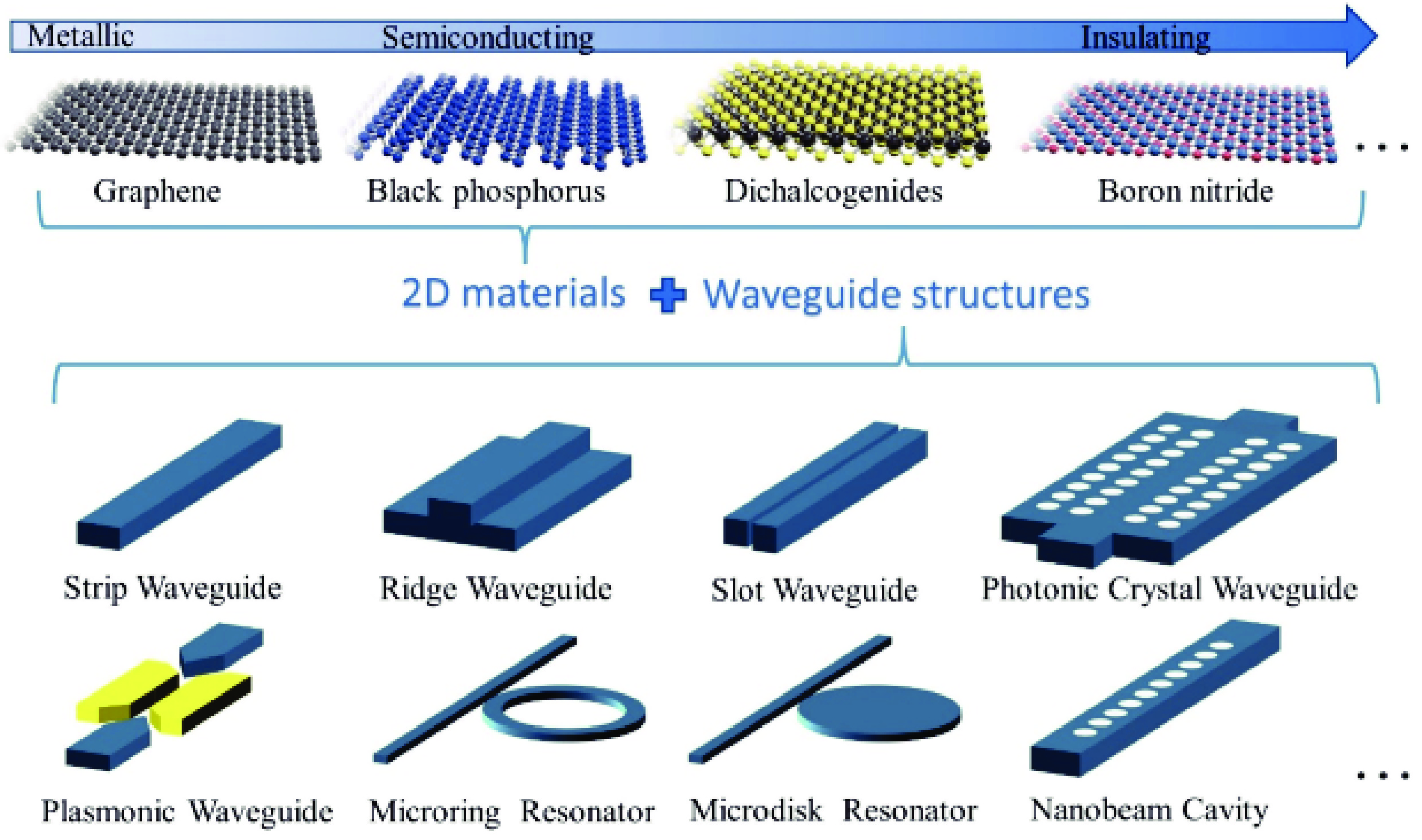
Fig. 1.  (Color online) Schematic illustration of on-chip waveguide-integrated optical modulation combing various 2D materials and diverse waveguide structures; the upper part shows typical 2D materials ranging from semimetals to insulators, and the lower part shows typical waveguide structures.

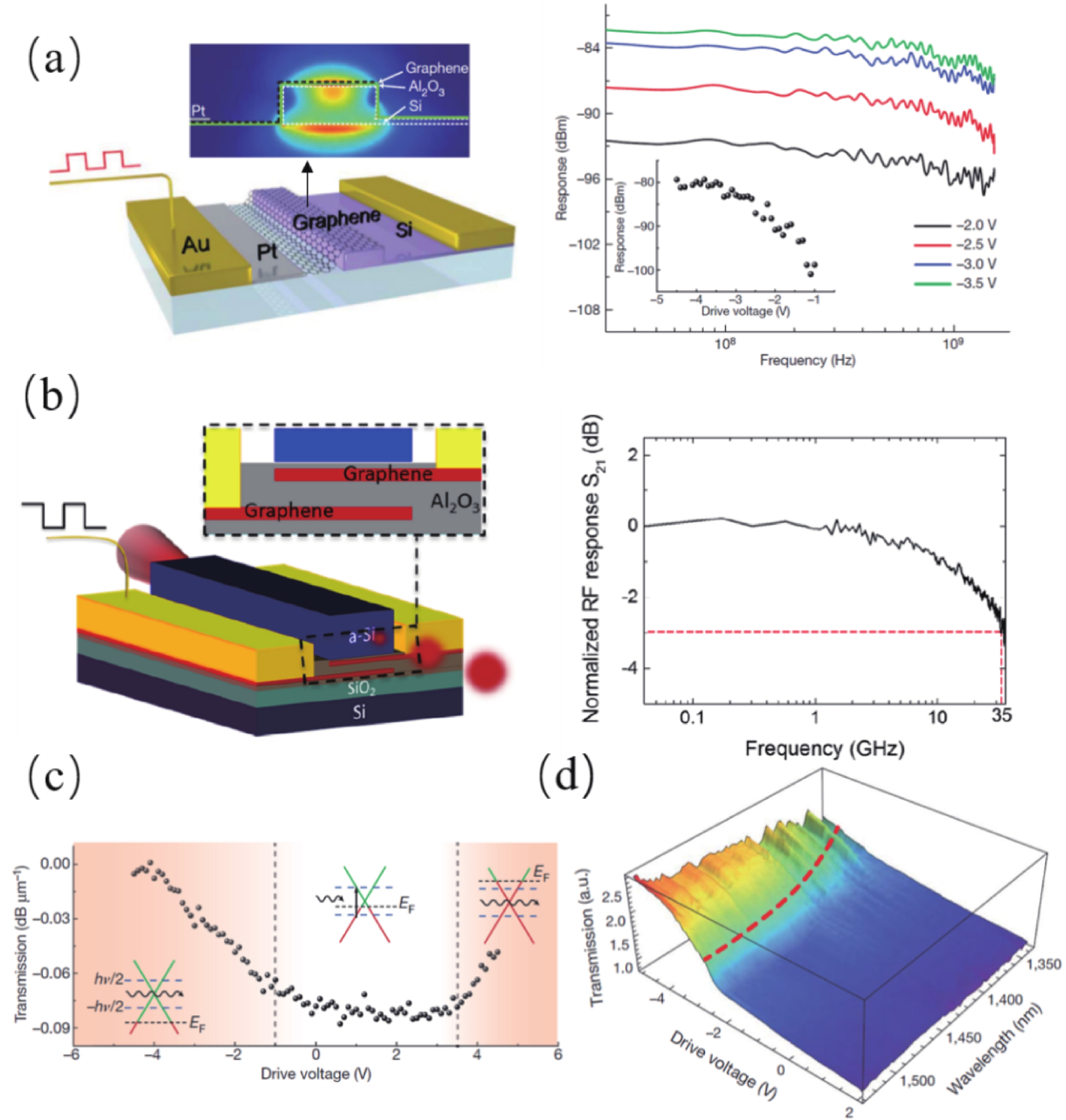
Fig. 2.  (Color online) Waveguide-integrated electro-optic modulators with non-resonant structures. (a) Schematic illustration of the first waveguide-integrated broadband electro-optic modulators based on graphene (left-hand) and the dynamic response of the device under different bias voltages (right-hand). The waveguide was optimized to carry a single mode and achieve a strong light–matter interaction in graphene[16]. (b) Schematic configuration of a waveguide-integrated electro-optic modulator based on two layers of graphene separated by a dielectric spacer (left-hand) and the measured RF response (right-hand)[52]. (c) The voltage-dependent static electro-optic response of a single graphene layer[16]. (d) The transmission spectra of the device shown in part (a) as a function of the driving voltage[16]. Figures reproduced with permission: (a, c, d) Ref. [16], © 2011 Nature Publishing Group, (b) Ref. [52], © 2016 American Chemical Society.

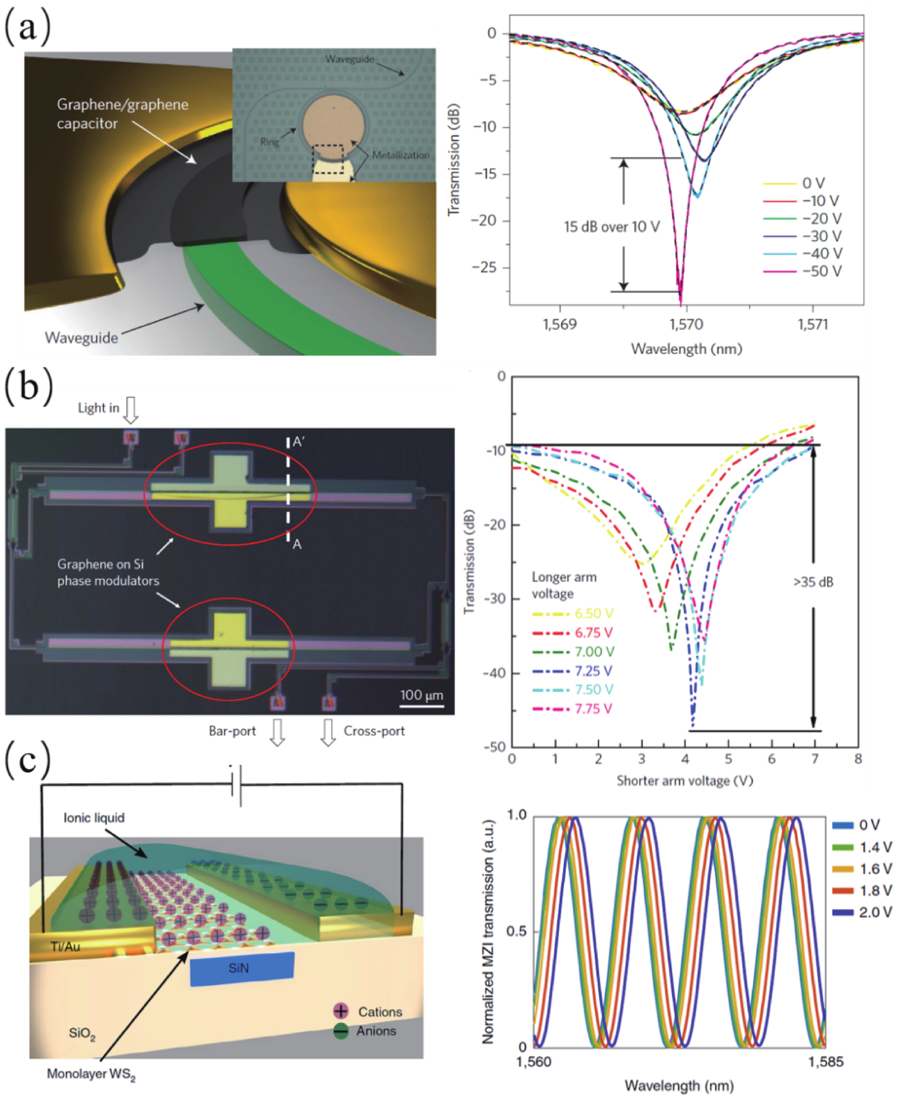
Fig. 3.  (Color online) Waveguide-integrated electro-optic modulators with resonant and interferometric structures. (a) Schematic illustration of an electro-optic modulator based on graphene-integrated MRR (left-hand) and its transmission spectra at different gate voltages (right)[60]. The upper–right-hand inset of the left-hand picture shows the microscope image of the fabricated structure. (b) Optical microscope image of a graphene-based modulator with an MZI structure (left-hand) and its transmission spectra at different gate voltages (right-hand)[85]. (c) Schematic illustration of a composite SiN-WS2 waveguide with ionic liquid ([P14+] [FAP−]) cladding used as an active region for electro-optic modulators based on an MZI structure (left-hand), and the transmission spectra of the device at different gate voltages (right-hand)[77]. Figures reproduced with permission: (a) Ref. [60], © 2015 Nature Publishing Group. (b) Ref. [85], © 2018 Nature Publishing Group. (c) Ref. [77], © 2020 Nature Publishing Group.

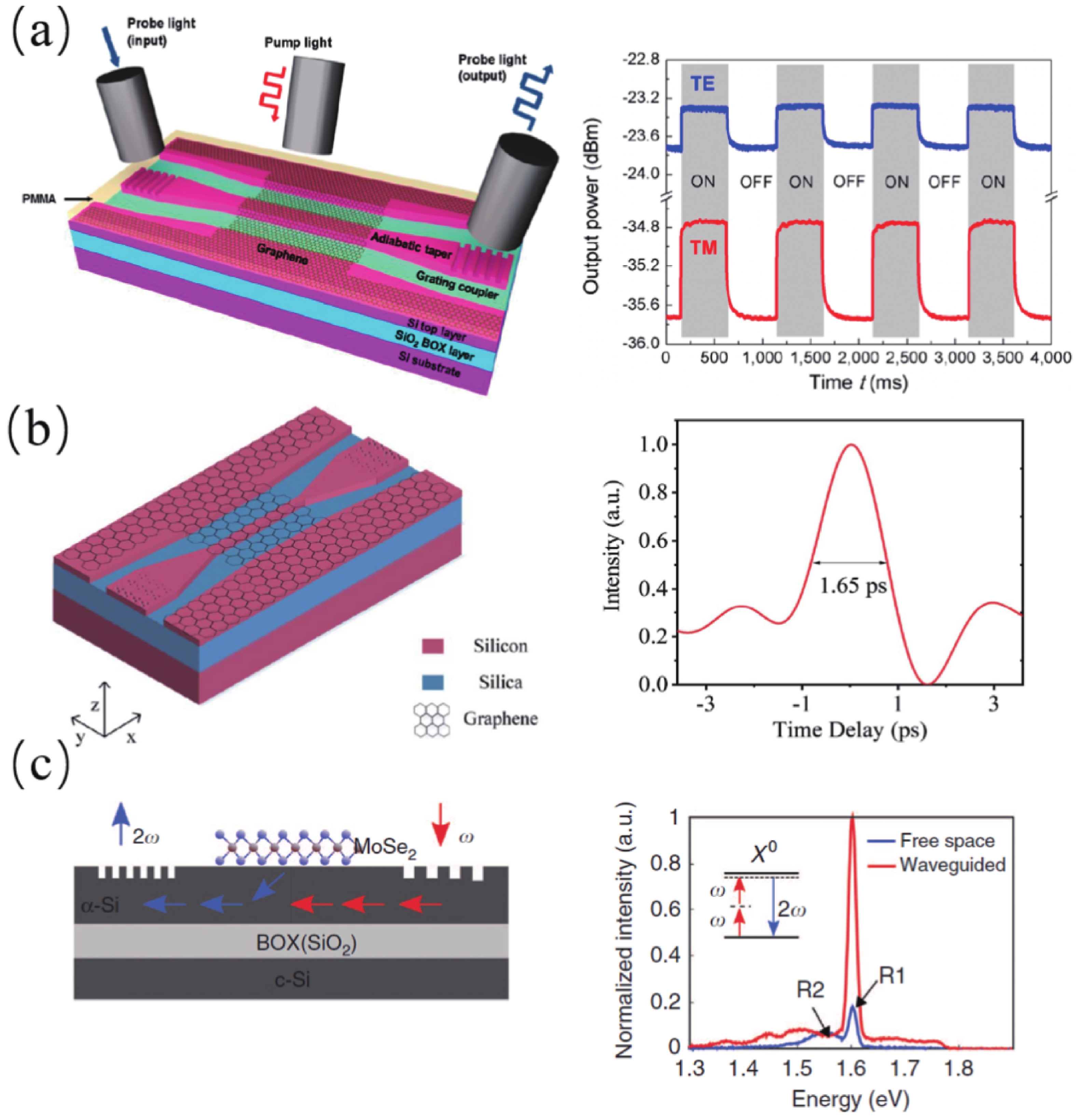
Fig. 4.  (Color online) Waveguide-integrated all-optical modulators with 2D materials. (a) Schematic illustration of a waveguide-integrated all-optical modulator with graphene based on the OIT effect (left-hand) and its dynamic response for different polarizations with a local modulated optical pump (right-hand)[115]. (b) Schematic structure of a waveguide-integrated all-optical modulator with graphene based on the saturable absorption effect (left-hand) and the transmission spectra of the probe light as a function of its time delay relative to the pump light (right-hand)[118]. (c) Schematic illustration of a waveguide-integrated all-optical wavelength converter based on monolayer MoSe2 (left-hand) and the measured second-harmonic generation signal from the waveguide-integrated structure compared to the free space excitation case (right-hand)[119]. Figures reproduced with permission: (a) Ref. [115], © 2014 American Chemical Society. (b) Ref. [118], © 2020 Chinese Laser Press. (c) Ref. [119], © 2017 Nature Publishing Group.

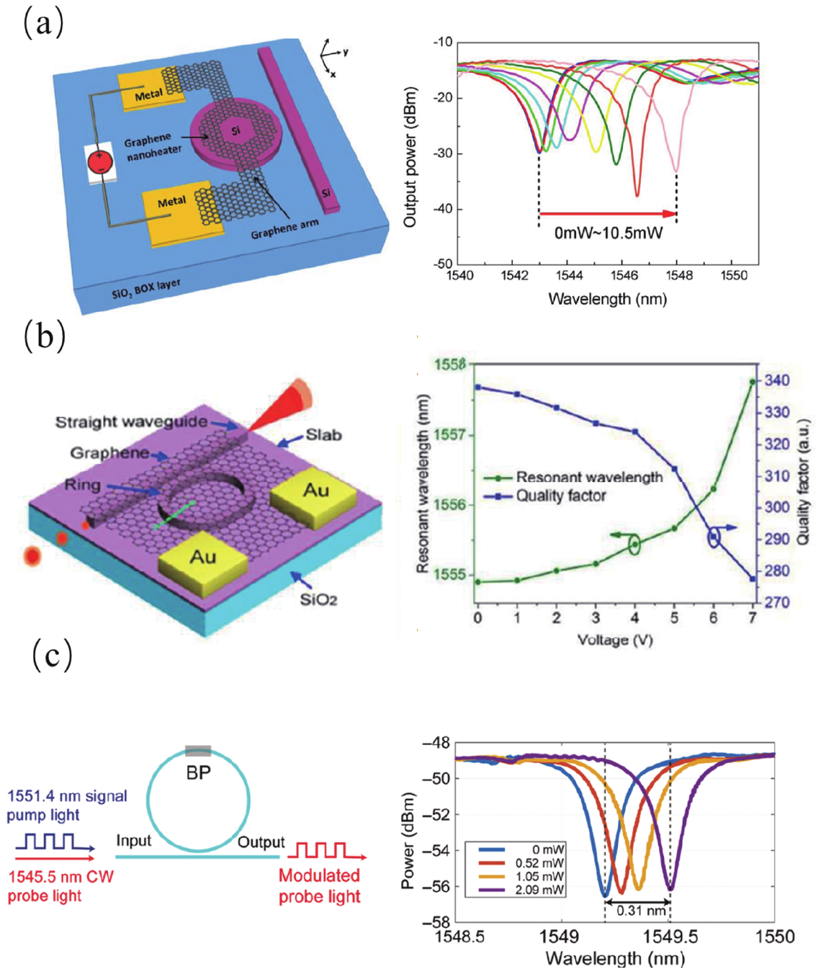
Fig. 5.  (Color online) Waveguide-integrated thermo-optic modulators based on 2D materials. (a) Schematic illustration of an optical modulator with a resonator using a graphene nano-heater (left-hand) and the output spectra of the device operating with different heating powers (right-hand)[139]. (b) Schematic illustration of a thermo-optic modulator with an MRR structure using a graphene heater (left-hand), and the measured resonant wavelength and the Q factor when operating at different applied voltages[61]. (c) Schematic illustration of a thermo-optic modulator with an MRR using the photothermal effect in BP (left-hand) and the measured resonant wavelength for different pumping powers (right-hand)[78]. Figures reproduced with permission: (a) Ref. [139], © 2014 AIP Publishing. (b) Ref. [61], © 2015 Royal Society of Chemistry. (c) Ref. [78], © 2020 De Gruyter.

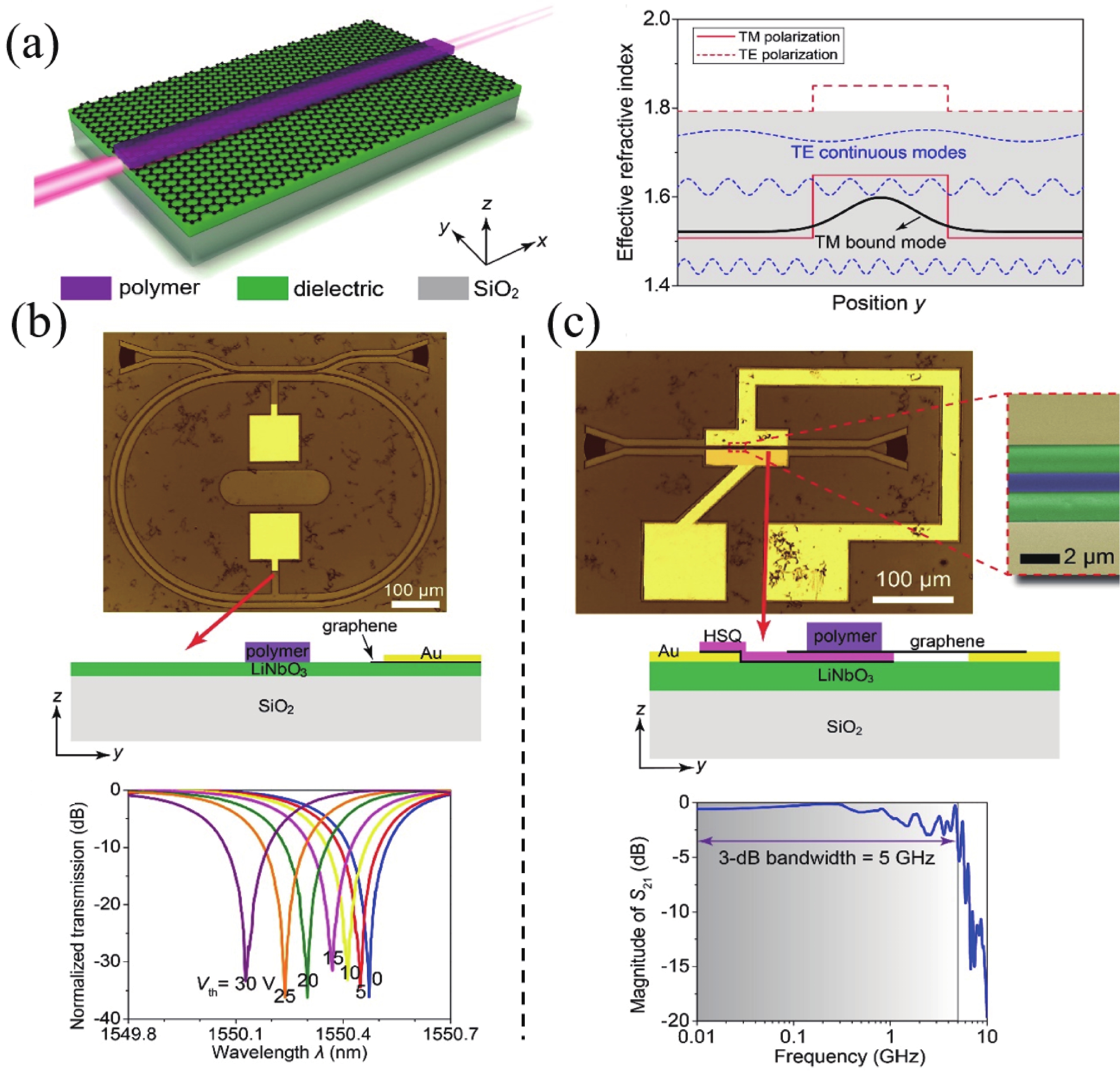
Fig. 6.  (Color online) Hybrid 2D materials modulation with BICs. (a) Conceptional illustration of the integration scheme based on BICs (left-hand) and the effective-refractive-index wells for the TE/TM polarizations of light at 1.55 µm in the hybrid waveguide (right-hand)[103]. (b) Optical microscope image and the cross-section of the fabricated thermo-optic modulator using graphene as heater based on the BICs scheme (upper part) and the measured transmission spectral response under different voltages (lower part)[103]. (c) Optical microscope image and the cross-section of the fabricated electro-optic modulator utilizing the electro-absorption effect of graphene based on the BICs scheme (upper part) and the measured frequency response (S21) of the device (lower part)[103]. Figures reproduced with permission: Ref. [103], © 2019 Wiley-VCH.

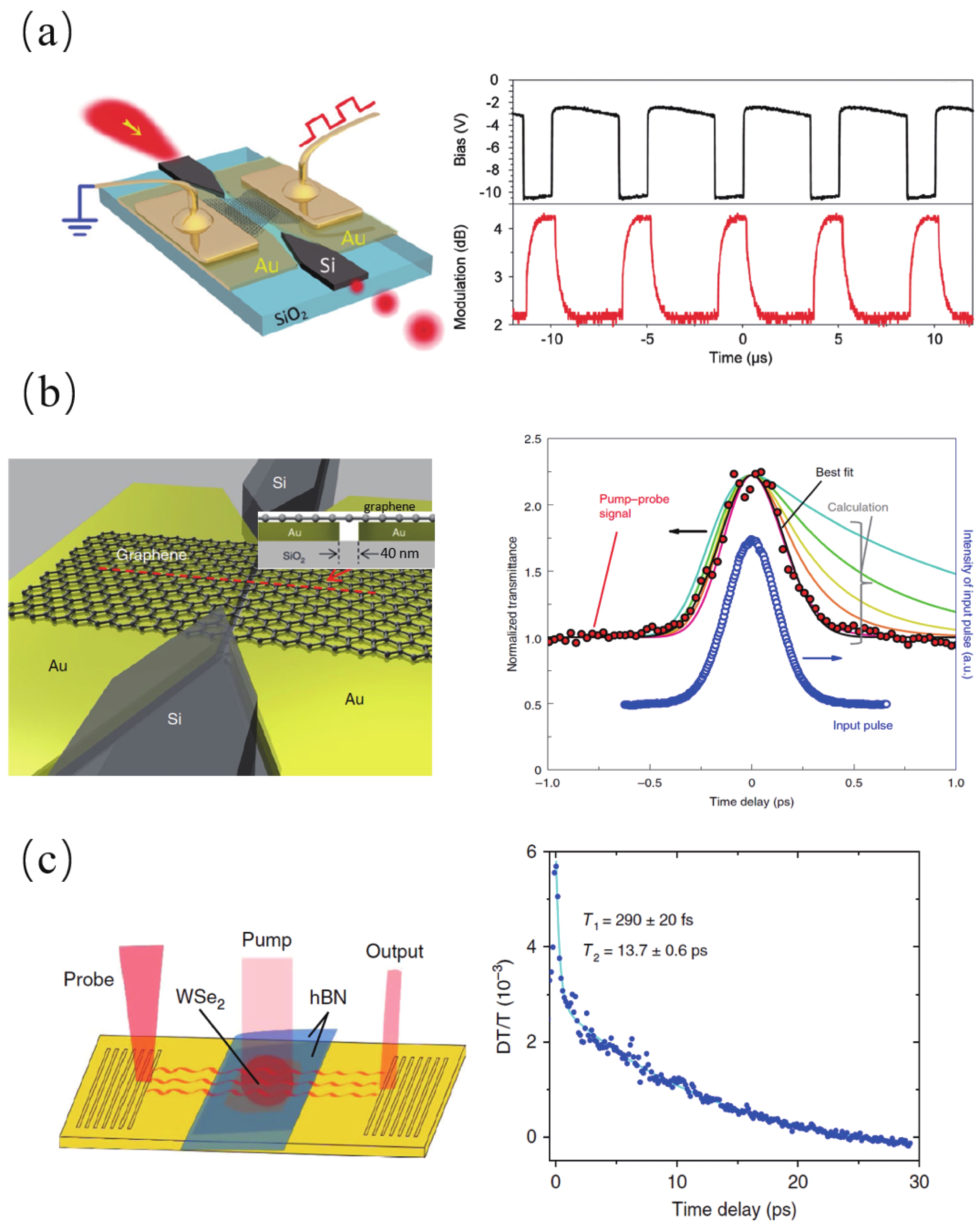
Fig. 7.  (Color online) Hybrid plasmonic waveguide optical modulators with 2D materials. (a) Schematic illustration of an electro-optic modulator with a plasmonic waveguide loaded with graphene (left-hand) and the output optical signal under modulated bias (right-hand)[58]. (b) Schematic illustration of an all-optical modulator based on a plasmonic waveguide loaded with graphene (left-hand) and its pump-probe response (right-hand)[59]. (c) Schematic illustration of an all-optical plasmonic modulator based on 2D semiconductors (left-hand) and the transient time response of the device (right-hand)[121]. Figures reproduced with permission: (a) Ref. [58], © 2017 Royal Society of Chemistry. (b) Ref. [59], © 2020 Nature Publishing Group. (c) Ref. [121], © 2019 Nature Publishing Group.

Table 1.   Performance of typical on-chip waveguide-integrated electro-optic modulators.

Materialsa) Structureb) Bandwidthc)
(GHz)
Modulation depth (dB) Insertion loss (dB) Energy consumption (fJ/bit) Drive voltage (V) Ref.d) Time
SL Gr Si waveguide 1.2 4 ~3.5 [16] 2011
BL Gr Si waveguide 1 6.5 4 ~5 [83] 2012
BL Gr Si waveguide 120* 2.9* 2.5* 8 [87] * 2012
ML Gr Si waveguide 100* 34* 17.6* [99] * 2014
BL Gr Si waveguide 1.8 16 3.3 6 [53] 2014
SL Gr Si MRR 80* 2.2* 6 [91] * 2014
BL Gr Si3N4 MRR 30 22 8.5 800 10 [60] 2015
SL Gr SiMRR 6.8 18 4 [92] 2015
Gr/hBN Si PhC cavity 1.2 3.2 2.5 [100] 2015
BL Gr a-Si waveguide 35 2 0.9 1400 25 [52] 2016
SL Gr Si waveguide 6 5 3.8 350 2.5 [101] 2016
BL Gr Si waveguide 120* π* 452* 6* [102] * 2017
BL Gr Plasmonic waveguide 0.13 dB/μm 7.5 [58] 2017
SL Gr Si MZI 5 35 1000 2 [85] 2018
BL Gr Dielectric waveguide 5 3 6 [103] 2019
SL WS2 Si3N4 MZI 0.3 3 8 [77] 2020
BL Gr Si waveguide 39 4.4 7.8 160 3.5 [86] 2021
BL Gr Si slot MRR > 40 33 5.8 6 [104] 2022
a) Gr, Graphene; SL, single layer; BL, bilayer; ML, multilayer; hBN, hexagonal boron nitride. b) MRR, microring resonator; PhC, photonic crystal; a-Si, amorphous silicon; MZI, Mach–Zehnder interferometer. c) Bandwidth indicates a 3 dB cutoff frequency. d) Values and references marked with * refer to the calculated results.
DownLoad: CSV

Table 2.   Performance of typical on-chip waveguide-integrated all-optical modulators.

Materialsa) Structuresb) Principlec) Response
time (ps)
Modulation depth (dB) energy consumptiond) Ref.e) Publication time
SL Gr Si waveguide OIT 1 2 W/cm2 [115] 2014
SL Gr Si PhC cavity OIT, hot carrier effects 10 kW/cm2 [57] 2015
SL WS2 Si3N4 waveguide PL > 10 [120] 2017
SL Gr Dielectric waveguide OIT 2.75 [1] 2018
SL WSe2 Plasmonic waveguide third-order nonlinearity 0.29 ~0.3 650 fJ/bit [121] 2019
SL Gr Plasmonic waveguide 2.1 [122] 2019
SL Gr Si waveguide SA 1.65 1.1 2100 fJ/bit [118] 2020
SL Gr Plasmonic waveguide SA 0.26 3.5 35 fJ/bit [59] 2020
SL Gr Plasmonic waveguide SA 0.03−0.12* 3.5* <600* fJ/bit [123]* 2021
Gr/hBN Si slot waveguide SA 0.6* 7.3* <326* fJ/bit [124]* 2022
a) Gr, Graphene; SL, single layer; hBN, hexagonal boron nitride. b) PhC, photonic crystal. c) OIT, optically induced transparency; PL, photoluminescence; SA, saturable absorption. d) The unit W/cm2 refers to the power density of the pumped light. e) Values and references marked with * refer to the calculated results.
DownLoad: CSV

Table 3.   Performance of typical on-chip waveguide-integrated thermo-optic modulators.

Materialsa) Scheme Structuresb) Rise/fall
time (μs) c)
Tuning efficiency
(nm/mW)
Ref. Time
SL Gr Electrothermal effect Si MZI 20/20 0.0636 [139] 2014
SL Gr Electrothermal effect Si MRR 0.75/0.8 0.104 [61] 2015
SL Gr Electrothermal effect Si MDR 12.8/8.8 1.67 [134] 2016
SL Gr Electrothermal effect ChG PhC cavity 14/− 10 [79] 2017
SL Gr Electrothermal effect Si PhC 0.75/0.525 1.07 [135] 2017
SL Gr Photothermal effect Si3N4 MRR 0.556/1.952 0.0079 [136] 2017
SL Gr Electrothermal effect Si PCNC 2.44/3.23 1.5 [62] 2017
BP film Photothermal effect Si MRR 0.479/0.113 0.0469 [78] 2020
b-AsP film Electrothermal effect Si MZI 30/20 0.74 [137] 2020
PtSe2 film photothermal effect Si MRR 304/284 0.004 [140] 2020
SL Gr photothermal effect Si MRR 0.2/1.5 0.216 [141] 2021
SL Gr photothermal effect Si PCNC 3.24/5.52 0.0346 [142] 2021
SL Gr photothermal effect Si3N4 MZI 1.25/2.83 0.0385 [143] 2021
SL Gr Electrothermal effect Si RTR 1.2/3.6 0.24 [144] 2022
MoTe2 film photothermal effect Si MDR 1.5/3.3 0.1584 [138] 2023
a) Gr, Graphene; SL, single layer; BP, black phosphorus; b-AsP, black arsenic-phosphorus; b) MZI, Mach–Zehnder interferometer; MRR, microring resonator; MDR, microdisk resonator; ChG, chalcogenide glass; PhC, photonic crystal; PCNC, photonic crystal nanobeam cavity; RTR, racetrack-type resonator. c) The rise/full time follows the 10%−90% rule.
DownLoad: CSV
[1]
Srivastava N, Banerjee K. Interconnect challenges for nanoscale electronic circuits. JOM, 2004, 56, 30 doi: 10.1007/s11837-004-0285-1
[2]
Inniss D, Rubenstein R. Silicon photonics: fueling the next information revolution. Morgan Kaufmann, 2016
[3]
Wang J, Long Y. On-chip silicon photonic signaling and processing: A review. Sci Bull, 2018, 63, 1267 doi: 10.1016/j.scib.2018.05.038
[4]
Thomson D, Zilkie A, Bowers J E, et al. Roadmap on silicon photonics. J Opt, 2016, 18, 073003 doi: 10.1088/2040-8978/18/7/073003
[5]
Guo D F, Hou K, Tang W J, et al. Silicon polarization switch based on symmetric polarization splitter-rotators. J Semicond, 2019, 40, 100401 doi: 10.1088/1674-4926/40/10/100401
[6]
Wang H M, Chai H Y, Lv Z R, et al. Silicon photonic transceivers for application in data centers. J Semicond, 2020, 41, 101301 doi: 10.1088/1674-4926/41/10/101301
[7]
Fu X, Dai D. Ultra-small Si-nanowire-based 400 GHz-spacing 15 × 15 arrayed-waveguide grating router with microbends. Electron Lett, 2011, 47, 266 doi: 10.1049/el.2010.3068
[8]
Bogaerts W, De Heyn P, Van Vaerenbergh T, et al. Silicon microring resonators. Laser Photonics Rev, 2012, 6, 47 doi: 10.1002/lpor.201100017
[9]
Dai D X, Bauters J, Bowers J E. Passive technologies for future large-scale photonic integrated circuits on silicon: Polarization handling, light non-reciprocity and loss reduction. Light Sci Appl, 2012, 1, e1 doi: 10.1038/lsa.2012.1
[10]
Dai D X, Liu L, Gao S M, et al. Polarization management for silicon photonic integrated circuits. Laser Photonics Rev, 2013, 7, 303 doi: 10.1002/lpor.201200023
[11]
Zhou Z P, Yin B, Michel J. On-chip light sources for silicon photonics. Light Sci Appl, 2015, 4, e358 doi: 10.1038/lsa.2015.131
[12]
Wang X, Su Z, Zhou Z. Recent progress of silicon photonics. Scientia Sinica Physica, 2015, 45, 014201 doi: 10.1360/SSPMA2014-00300
[13]
Bogaerts W, Chrostowski L. Silicon photonics circuit design: Methods, tools and challenges. Laser Photonics Rev, 2018, 12, 1700237 doi: 10.1002/lpor.201700237
[14]
Liu S T, Khope A. Latest advances in high-performance light sources and optical amplifiers on silicon. J Semicond, 2021, 42, 041307 doi: 10.1088/1674-4926/42/4/041307
[15]
Reed G T, Mashanovich G, Gardes F Y, et al. Silicon optical modulators. Nature Photon, 2010, 4, 518 doi: 10.1038/nphoton.2010.179
[16]
Liu M, Yin X B, Ulin-Avila E, et al. A graphene-based broadband optical modulator. Nature, 2011, 474, 64 doi: 10.1038/nature10067
[17]
Sun Z P, Martinez A, Wang F. Optical modulators with 2D layered materials. Nature Photon, 2016, 10, 227 doi: 10.1038/nphoton.2016.15
[18]
Dai D X, Li J, Yin Y L. Silicon-plus photonics for light manipulation and photodetection. Proc. SPIE 10812, Semiconductor Lasers and Applications VIII, 2018, 1082 doi: 10.1117/12.2503373
[19]
Wang X X, Liu J F. Emerging technologies in Si active photonics. J Semicond, 2018, 39, 061001 doi: 10.1088/1674-4926/39/6/061001
[20]
Su Y K, Zhang Y, Qiu C Y, et al. Silicon photonic platform for passive waveguide devices: Materials, fabrication, and applications. Adv Mater Technol, 2020, 5, 1901153 doi: 10.1002/admt.201901153
[21]
Marris-Morini D, Vakarin V, Ramirez J M, et al. Germanium-based integrated photonics from near- to mid-infrared applications. Nanophotonics, 2018, 7, 1781 doi: 10.1515/nanoph-2018-0113
[22]
Ramirez J M, Elfaiki H, Verolet T, et al. III-V-on-silicon integration: From hybrid devices to heterogeneous photonic integrated circuits. IEEE J Sel Top Quantum Electron, 2020, 26, 1 doi: 10.1109/JSTQE.2019.2939503
[23]
Semond F. Epitaxial challenges of GaN on silicon. MRS Bull, 2015, 40, 412 doi: 10.1557/mrs.2015.96
[24]
Novoselov K S, Geim A K, Morozov S V, et al. Electric field effect in atomically thin carbon films. Science, 2004, 306, 666 doi: 10.1126/science.1102896
[25]
Geim A K. Graphene: Status and prospects. Science, 2009, 324, 1530 doi: 10.1126/science.1158877
[26]
Schaibley J R, Yu H Y, Clark G, et al. Valleytronics in 2D materials. Nat Rev Mater, 2016, 1, 16055 doi: 10.1038/natrevmats.2016.55
[27]
Manzeli S, Ovchinnikov D, Pasquier D, et al. 2D transition metal dichalcogenides. Nat Rev Mater, 2017, 2, 17033 doi: 10.1038/natrevmats.2017.33
[28]
Chen H, Liu M, Xu L, et al. Valley-selective directional emission from a transition-metal dichalcogenide monolayer mediated by a plasmonic nanoantenna, Beilstein. J. Nanotechnol, 2018, 9, 780 doi: 10.3762/bjnano.9.71
[29]
Jiang T, Yin K, Wang C, et al. Ultrafast fiber lasers mode-locked by two-dimensional materials: review and prospect. Photonics Research, 2020, 8(1), 78 doi: 10.1364/PRJ.8.000078
[30]
Novoselov K S, Geim A K, Morozov S V, et al. Two-dimensional gas of massless Dirac fermions in graphene. Nature, 2005, 438, 197 doi: 10.1038/nature04233
[31]
Xia F N, Wang H, Xiao D, et al. Two-dimensional material nanophotonics. Nat Photonics, 2014, 8, 899 doi: 10.1038/nphoton.2014.271
[32]
Caldwell J D, Aharonovich I, Cassabois G, et al. Photonics with hexagonal boron nitride. Nat Rev Mater, 2019, 4, 552 doi: 10.1038/s41578-019-0124-1
[33]
Luo M M, Fan T J, Zhou Y, et al. 2D black phosphorus–based biomedical applications. Adv Funct Mater, 2019, 29, 1808306 doi: 10.1002/adfm.201808306
[34]
Acun A, Zhang L, Bampoulis P, et al. Germanene: The germanium analogue of graphene. J Phys: Condens Matter, 2015, 27, 443002 doi: 10.1088/0953-8984/27/44/443002
[35]
Youngblood N, Li M. Integration of 2D materials on a silicon photonics platform for optoelectronics applications. Nanophotonics, 2016, 6, 1205 doi: 10.1515/nanoph-2016-0155
[36]
Akinwande D, Huyghebaert C, Wang C H, et al. Graphene and two-dimensional materials for silicon technology. Nature, 2019, 573, 507 doi: 10.1038/s41586-019-1573-9
[37]
Yin Y L, Li J, Xu Y, et al. Silicon-graphene photonic devices. J Semicond, 2018, 39, 061009 doi: 10.1088/1674-4926/39/6/061009
[38]
Dai D X, Li J, Song L J. Silicon-plus photonic devices for on-chip light-manipulation and photodetection. Proc. SPIE 11182, Semiconductor Lasers and Applications IX, 2019, 1118206 doi: 10.1117/12.2538255
[39]
Tang Y H, Mak K F. 2D materials for silicon photonics. Nature Nanotech, 2017, 12, 1121 doi: 10.1038/nnano.2017.230
[40]
Chen H T, Nanz S, Abass A, et al. Enhanced directional emission from monolayer WSe2 integrated onto a multiresonant silicon-based photonic structure. ACS Photonics, 2017, 4, 3031 doi: 10.1021/acsphotonics.7b00550
[41]
Ross J S, Wu S F, Yu H Y, et al. Electrical control of neutral and charged excitons in a monolayer semiconductor. Nat Commun, 2013, 4, 1474 doi: 10.1038/ncomms2498
[42]
Ross J S, Klement P, Jones A M, et al. Electrically tunable excitonic light-emitting diodes based on monolayer WSe2 p–n junctions. Nat Nanotechnol, 2014, 9, 268 doi: 10.1038/nnano.2014.26
[43]
Yang J, Xu R J, Pei J J, et al. Optical tuning of exciton and trion emissions in monolayer phosphorene. Light Sci Appl, 2015, 4, e312 doi: 10.1038/lsa.2015.85
[44]
Ouyang H, Chen H T, Tang Y X, et al. All-optical dynamic tuning of local excitonic emission of monolayer MoS2 by integration with Ge2Sb2Te5. Nanophotonics, 2020, 9, 2351 doi: 10.1515/nanoph-2019-0366
[45]
Mouri S, Miyauchi Y, Matsuda K. Tunable photoluminescence of monolayer MoS2 via chemical doping. Nano Lett, 2013, 13, 5944 doi: 10.1021/nl403036h
[46]
Li Z W, Lv Y W, Ren L W, et al. Efficient strain modulation of 2D materials via polymer encapsulation. Nat Commun, 2020, 11, 1151 doi: 10.1038/s41467-020-15023-3
[47]
Novoselov K S, Mishchenko A, Carvalho A, et al. 2D materials and van der Waals heterostructures. Science, 2016, 353(6298), aac9439 doi: 10.1126/science.aac9439
[48]
Liu Y, Weiss N O, Duan X D, et al. Van der waals heterostructures and devices. Nat Rev Mater, 2016, 1, 16042 doi: 10.1038/natrevmats.2016.42
[49]
Gibertini M, Koperski M, Morpurgo A F, et al. Magnetic 2D materials and heterostructures. Nat Nanotechnol, 2019, 14, 408 doi: 10.1038/s41565-019-0438-6
[50]
Wei K, Jiang T, Xu Z J, et al. Hybrid perovskites: Ultrafast carrier transfer promoted by interlayer coulomb coupling in 2D/3D perovskite heterostructures (laser photonics rev. 12(10)/2018). Laser Photonics Rev, 2018, 12, 1870043 doi: 10.1002/lpor.201870043
[51]
Wei K, Sui Y Z, Xu Z J, et al. Acoustic phonon recycling for photocarrier generation in graphene-WS2 heterostructures. Nat Commun, 2020, 11, 3876 doi: 10.1038/s41467-020-17728-x
[52]
Dalir H, Xia Y, Wang Y, et al. Athermal broadband graphene optical modulator with 35 GHz speed. ACS Photonics, 2016, 3, 1564 doi: 10.1021/acsphotonics.6b00398
[53]
Mohsin M, Schall D, Otto M, et al. Graphene based low insertion loss electro-absorption modulator on SOI waveguide. Opt Express, 2014, 22, 15292 doi: 10.1364/OE.22.015292
[54]
Lu Z L, Zhao W S. Nanoscale electro-optic modulators based on graphene-slot waveguides. J Opt Soc Am B, 2012, 29, 1490 doi: 10.1364/JOSAB.29.001490
[55]
Jiao J Y, Hao R, Zhen Z, et al. Optimization of graphene-based slot waveguides for efficient modulation. IEEE J Sel Top Quantum Electron, 2020, 26, 1 doi: 10.1109/JSTQE.2019.2941469
[56]
Cheng Z, Zhu X L, Galili M, et al. Double-layer graphene on photonic crystal waveguide electro-absorption modulator with 12 GHz bandwidth. Nanophotonics, 2020, 9, 2377 doi: 10.1515/nanoph-2019-0381
[57]
Shi Z, Gan L, Xiao T H, et al. All-optical modulation of a graphene-cladded silicon photonic crystal cavity. ACS Photonics, 2015, 2, 1513 doi: 10.1021/acsphotonics.5b00469
[58]
Ding Y, Guan X, Zhu X, et al. Efficient electro-optic modulation in low-loss graphene-plasmonic slot waveguides. Nanoscale, 2017, 9, 15576 doi: 10.1039/C7NR05994A
[59]
Ono M, Hata M, Tsunekawa M, et al. Ultrafast and energy-efficient all-optical switching with graphene-loaded deep-subwavelength plasmonic waveguides. Nat Photonics, 2020, 14, 37 doi: 10.1038/s41566-019-0547-7
[60]
Phare C T, Lee Y H D, Cardenas J, et al. Graphene electro-optic modulator with 30 GHz bandwidth. Nat Photonics, 2015, 9, 511 doi: 10.1038/nphoton.2015.122
[61]
Gan S, Cheng C T, Zhan Y H, et al. A highly efficient thermo-optic microring modulator assisted by graphene. Nanoscale, 2015, 7, 20249 doi: 10.1039/C5NR05084G
[62]
Xu Z Z, Qiu C Y, Yang Y X, et al. Ultra-compact tunable silicon nanobeam cavity with an energy-efficient graphene micro-heater. Opt Express, 2017, 25, 19479 doi: 10.1364/OE.25.019479
[63]
Jafari Z, Zarifkar A, Miri M, et al. All-optical modulation in a graphene-covered slotted silicon nano-beam cavity. J Light Technol, 2018, 36, 4051 doi: 10.1109/JLT.2018.2858551
[64]
Chai Z, Hu X, Wang F, et al. Ultrafast All-Optical Switching. Adv Opt Mater, 2017, 5(7), 1600665 doi: 10.1002/adom.201600665
[65]
Yao Y H, Cheng Z, Dong J J, et al. Performance of integrated optical switches based on 2D materials and beyond. Front Optoelectron, 2020, 13, 129 doi: 10.1007/s12200-020-1058-3
[66]
Yu S L, Wu X Q, Wang Y P, et al. 2D materials for optical modulation: Challenges and opportunities. Adv Mater, 2017, 29, 1606128 doi: 10.1002/adma.201606128
[67]
Chen H T, Wang C, Ouyang H, et al. All-optical modulation with 2D layered materials: Status and prospects. Nanophotonics, 2020, 9, 2107 doi: 10.1515/nanoph-2019-0493
[68]
You J, Luo Y K, Yang J, et al. Hybrid/integrated silicon photonics based on 2D materials in optical communication nanosystems. Laser Photonics Rev, 2020, 14, 2000239 doi: 10.1002/lpor.202000239
[69]
Gan X, Englund D, Van Thourhout D, et al. 2D materials-enabled optical modulators: From visible to terahertz spectral range. Appl Phys Rev, 2022, 9(2), 021302 doi: 10.1063/5.0078416
[70]
Yang H Y, Wang Y Z, Tiu Z C, et al. All-optical modulation technology based on 2D layered materials. Micromachines, 2022, 13, 92 doi: 10.3390/mi13010092
[71]
Wang G Z, Baker-Murray A A, Blau W J. Saturable absorption in 2D nanomaterials and related photonic devices. Laser Photonics Rev, 2019, 13, 1800282 doi: 10.1002/lpor.201800282
[72]
Li Q, Lu J, Gupta P, et al. Engineering optical absorption in graphene and other 2D materials: Advances and applications. Adv Opt Mater, 2019, 7, 1900595 doi: 10.1002/adom.201900595
[73]
Cheng J L, Sipe J E, Vermeulen N, et al. Nonlinear optics of graphene and other 2D materials in layered structures. J Phys Photonics, 2018, 1, 015002 doi: 10.1088/2515-7647/aaeadb
[74]
Wu K, Wang Y F, Qiu C Y, et al. Thermo-optic all-optical devices based on two-dimensional materials. Photon Res, 2018, 6, C22 doi: 10.1364/PRJ.6.000C22
[75]
Optical modulation. Cambridge University Press, Cambridge, 2016
[76]
Miller D A B. Energy consumption in optical modulators for interconnects. Opt Express, 2012, 20, A293 doi: 10.1364/OE.20.00A293
[77]
Datta I, Chae S H, Bhatt G R, et al. Low-loss composite photonic platform based on 2D semiconductor monolayers. Nat Photonics, 2020, 14, 256 doi: 10.1038/s41566-020-0590-4
[78]
Cheng Z, Cao R, Guo J, et al. Phosphorene-assisted silicon photonic modulator with fast response time. Nanophotonics, 2020, 9, 1973 doi: 10.1515/nanoph-2019-0510
[79]
Lin H T, Song Y, Huang Y Z, et al. Chalcogenide glass-on-graphene photonics. Nature Photon, 2017, 11, 798 doi: 10.1038/s41566-017-0033-z
[80]
Bao X Z, Ou Q D, Xu Z Q, et al. Band structure engineering in 2D materials for optoelectronic applications. Adv Mater Technol, 2018, 3, 1800072 doi: 10.1002/admt.201800072
[81]
Wang F, Zhang Y B, Tian C S, et al. Gate-variable optical transitions in graphene. Science, 2008, 320, 206 doi: 10.1126/science.1152793
[82]
Liu Y P, Tom K, Wang X, et al. Dynamic control of optical response in layered metal chalcogenide nanoplates. Nano Lett, 2016, 16, 488 doi: 10.1021/acs.nanolett.5b04140
[83]
Liu M, Yin X B, Zhang X. Double-layer graphene optical modulator. Nano Lett, 2012, 12, 1482 doi: 10.1021/nl204202k
[84]
Youngblood N, Anugrah Y, Ma R, et al. Multifunctional graphene optical modulator and photodetector integrated on silicon waveguides. Nano Lett, 2014, 14, 2741 doi: 10.1021/nl500712u
[85]
Sorianello V, Midrio M, Contestabile G, et al. Graphene–silicon phase modulators with gigahertz bandwidth. Nat Photonics, 2018, 12, 40 doi: 10.1038/s41566-017-0071-6
[86]
Agarwal H, Terrés B, Orsini L, et al. 2D-3D integration of hexagonal boron nitride and a high-κ dielectric for ultrafast graphene-based electro-absorption modulators. Nat Commun, 2021, 12, 1 doi: 10.1038/s41467-020-20314-w
[87]
Koester S J, Li M. High-speed waveguide-coupled graphene-on-graphene optical modulators. Appl Phys Lett, 2012, 100, 171107. doi: 10.1063/1.4704663
[88]
Hao R, Jin J M. Graphene embedded modulator with extremely small footprint and high modulation efficiency. J Photonics, 2014, 2014, 309350 doi: 10.1155/2014/309350
[89]
Hao R, Ye Z W, Gu Y J, et al. Large modulation capacity in graphene-based slot modulators by enhanced hybrid plasmonic effects. Sci Rep, 2018, 8, 16830 doi: 10.1038/s41598-018-34914-6
[90]
Midrio M, Galli P, Romagnoli M, et al. Graphene-based optical phase modulation of waveguide transverse electric modes. Photon Res, 2014, 2, A34 doi: 10.1364/PRJ.2.000A34
[91]
Qiu C Y, Gao W L, Vajtai R, et al. Efficient modulation of 1.55 μm radiation with gated graphene on a silicon microring resonator. Nano Lett, 2014, 14, 6811 doi: 10.1021/nl502363u
[92]
Ding Y H, Zhu X L, Xiao S S, et al. Effective electro-optical modulation with high extinction ratio by a graphene–silicon microring resonator. Nano Lett, 2015, 15, 4393 doi: 10.1021/acs.nanolett.5b00630
[93]
Luo S Y, Wang Y N, Tong X, et al. Graphene-based optical modulators. Nanoscale Res Lett, 2015, 10, 1 doi: 10.1186/1556-276X-10-1
[94]
Shi Y X, Li J S, Zhang L. Graphene-integrated split-ring resonator terahertz modulator. Opt Quantum Electron, 2017, 49, 350 doi: 10.1007/s11082-017-1198-x
[95]
Xu C, Jin Y C, Yang L Z, et al. Characteristics of electro-refractive modulating based on graphene-oxide-silicon waveguide. Opt Express, 2012, 20, 22398 doi: 10.1364/OE.20.022398
[96]
Yang L Z, Hu T, Hao R, et al. Low-chirp high-extinction-ratio modulator based on graphene–silicon waveguide. Opt Lett, 2013, 38, 2512 doi: 10.1364/OL.38.002512
[97]
Hao R, Du W, Chen H S, et al. Ultra-compact optical modulator by graphene induced electro-refraction effect. Appl Phys Lett, 2013, 103, 061161 doi: 10.1063/1.4818457
[98]
Mohsin M, Neumaier D, Schall D, et al. Experimental verification of electro-refractive phase modulation in graphene. Sci Rep, 2015, 5, 10967 doi: 10.1038/srep10967
[99]
Ye S W, Wang Z S, Tang L F, et al. Electro-absorption optical modulator using dual-graphene-on-graphene configuration. Opt Express, 2014, 22, 26173 doi: 10.1364/OE.22.026173
[100]
Gao Y D, Shiue R J, Gan X T, et al. High-speed electro-optic modulator integrated with graphene-boron nitride heterostructure and photonic crystal nanocavity. Nano Lett, 2015, 15, 2001 doi: 10.1021/nl504860z
[101]
Hu Y T, Pantouvaki M, Van Campenhout J, et al. Broadband 10 Gb/s operation of graphene electro-absorption modulator on silicon. Laser Photonics Rev, 2016, 10, 307 doi: 10.1002/lpor.201500250
[102]
Ye S W, Yuan F, Zou X H, et al. High-speed optical phase modulator based on graphene-silicon waveguide. IEEE J Sel Top Quantum Electron, 2017, 23, 76 doi: 10.1109/JSTQE.2016.2545238
[103]
Yu Z J, Wang Y, Sun B L, et al. Hybrid 2D-material photonics with bound states in the continuum. Adv Optical Mater, 2019, 7, 1901306 doi: 10.1002/adom.201901306
[104]
Luan C, Kong D M, Ding Y H, et al. High-modulation-efficiency graphene-silicon slot-waveguide micro-ring modulator. Conference on Lasers and Electro-Optics, San Jose, 2022 doi: 10.1364/CLEO_AT.2022.JTh6B.8
[105]
Gosciniak J, Tan D T H. Theoretical investigation of graphene-based photonic modulators. Sci Rep, 2013, 3, 1897 doi: 10.1038/srep01897
[106]
Gan X T, Zhao C Y, Wang Y D, et al. Graphene-assisted all-fiber phase shifter and switching. Optica, 2015, 2, 468 doi: 10.1364/OPTICA.2.000468
[107]
Lee E J, Choi S Y, Jeong H, et al. Active control of all-fibre graphene devices with electrical gating. Nat Commun, 2015, 6, 6851 doi: 10.1038/ncomms7851
[108]
Hu Y Z, You J, Tong M Y, et al. Metaphotonic devices: Pump-color selective control of ultrafast all-optical switching dynamics in metaphotonic devices (adv. sci. 14/2020). Adv Sci, 2020, 7, 2070080 doi: 10.1002/advs.202070080
[109]
Bao Q L, Zhang H, Wang Y, et al. Atomic-layer graphene as a saturable absorber for ultrafast pulsed lasers. Adv Funct Mater, 2009, 19, 3077 doi: 10.1002/adfm.200901007
[110]
Sun Z P, Hasan T, Torrisi F, et al. Graphene mode-locked ultrafast laser. ACS Nano, 2010, 4, 803 doi: 10.1021/nn901703e
[111]
Zhang B T, Liu J, Wang C, et al. Recent progress in 2D material-based saturable absorbers for all solid-state pulsed bulk lasers. Laser Photonics Rev, 2020, 14, 1900240 doi: 10.1002/lpor.201900240
[112]
Hendry E, Hale P J, Moger J, et al. Coherent nonlinear optical response of graphene. Phys Rev Lett, 2010, 105, 097401 doi: 10.1103/PhysRevLett.105.097401
[113]
Wang J, Hernandez Y, Lotya M, et al. Broadband nonlinear optical response of graphene dispersions. Adv Mater, 2009, 21, 2430 doi: 10.1002/adma.200803616
[114]
Bao Q L, Zhang H, Wang B, et al. Broadband graphene polarizer. Nat Photonics, 2011, 5, 411 doi: 10.1038/nphoton.2011.102
[115]
Yu L H, Zheng J J, Xu Y, et al. Local and nonlocal optically induced transparency effects in graphene–silicon hybrid nanophotonic integrated circuits. ACS Nano, 2014, 8, 11386 doi: 10.1021/nn504377m
[116]
Ooi K J A, Leong P C, Ang L K, et al. All-optical control on a graphene-on-silicon waveguide modulator. Sci Rep, 2017, 7, 1 doi: 10.1038/s41598-016-0028-x
[117]
Demongodin P, El Dirani H, Lhuillier J, et al. Ultrafast saturable absorption dynamics in hybrid graphene/Si3N4 waveguides. APL Photonics, 2019, 4, 076102 doi: 10.1063/1.5094523
[118]
Wang H, Yang N N, Chang L M, et al. CMOS-compatible all-optical modulator based on the saturable absorption of graphene. Photon Res, 2020, 8, 468 doi: 10.1364/PRJ.380170
[119]
Chen H T, Corboliou V, Solntsev A S, et al. Enhanced second-harmonic generation from two-dimensional MoSe2 on a silicon waveguide. Light Sci Appl, 2017, 6, e17060 doi: 10.1038/lsa.2017.60
[120]
Yang S, Liu D C, Tan Z L, et al. CMOS-compatible WS2-based all-optical modulator. ACS Photonics, 2018, 5, 342 doi: 10.1021/acsphotonics.7b01206
[121]
Klein M, Badada B H, Binder R, et al. 2D semiconductor nonlinear plasmonic modulators. Nat Commun, 2019, 10, 3264 doi: 10.1038/s41467-019-11186-w
[122]
Sun F Y, Xia L P, Nie C B, et al. An all-optical modulator based on a graphene–plasmonic slot waveguide at 1550 nm. Appl Phys Express, 2019, 12, 042009 doi: 10.7567/1882-0786/ab0a89
[123]
Sun F Y, Xia L P, Nie C B, et al. The all-optical modulator in dielectric-loaded waveguide with graphene-silicon heterojunction structure. Nanotechnology, 2018, 29, 135201 doi: 10.1088/1361-6528/aaa8be
[124]
Alaloul M, Khurgin J B. High-performance all-optical modulator based on graphene-HBN heterostructures. IEEE J Sel Top Quantum Electron, 2022, 28, 1 doi: 10.1109/JSTQE.2022.3206066
[125]
Yu S L, Meng C, Chen B G, et al. Graphene decorated microfiber for ultrafast optical modulation. Opt Express, 2015, 23, 10764 doi: 10.1364/OE.23.010764
[126]
Li W, Chen B G, Meng C, et al. Ultrafast all-optical graphene modulator. Nano Lett, 2014, 14, 955 doi: 10.1021/nl404356t
[127]
Sun D, Wu Z K, Divin C, et al. Ultrafast relaxation of excited Dirac fermions in epitaxial graphene using optical differential transmission spectroscopy. Phys Rev Lett, 2008, 101, 157402 doi: 10.1103/PhysRevLett.101.157402
[128]
Dong P, Qian W, Liang H, et al. Thermally tunable silicon racetrack resonators with ultralow tuning power. Opt Express, 2010, 18, 20298 doi: 10.1364/OE.18.020298
[129]
Dong P, Shafiiha R, Liao S R, et al. Wavelength-tunable silicon microring modulator. Opt Express, 2010, 18, 10941 doi: 10.1364/OE.18.010941
[130]
Renteria J, Nika D, Balandin A. Graphene thermal properties: Applications in thermal management and energy storage. Appl Sci, 2014, 4, 525 doi: 10.3390/app4040525
[131]
Kang J M, Kim H, Kim K S, et al. High-performance graphene-based transparent flexible heaters. Nano Lett, 2011, 11, 5154 doi: 10.1021/nl202311v
[132]
Yu L H, Shi Y C, He S L, et al. Tunable silicon micro-disk resonator with flexible graphene-based ultra-thin heaters. Asia Communications and Photonics Conference 2015, 2015, AS3B. 2
[133]
Yu L, He S, Zheng J, et al. Graphene-based transparent nano-heater for thermally-tuning silicon nanophotonic integrated devices. Progress in Electromagnetics Research Symposium, 2014, 1735
[134]
Yu L H, Yin Y L, Shi Y C, et al. Thermally tunable silicon photonic microdisk resonator with transparent graphene nanoheaters. Optica, 2016, 3, 159 doi: 10.1364/OPTICA.3.000159
[135]
Yan S Q, Zhu X L, Frandsen L H, et al. Slow-light-enhanced energy efficiency for graphene microheaters on silicon photonic crystal waveguides. Nat Commun, 2017, 8, 14411 doi: 10.1038/ncomms14411
[136]
Qiu C Y, Yang Y X, Li C, et al. All-optical control of light on a graphene-on-silicon nitride chip using thermo-optic effect. Sci Rep, 2017, 7, 17046 doi: 10.1038/s41598-017-16989-9
[137]
Liu Y J, Wang H D, Wang S, et al. Highly efficient silicon photonic microheater based on black arsenic–phosphorus. Adv Optical Mater, 2020, 8, 1901526 doi: 10.1002/adom.201901526
[138]
Cao H Y, Chen H T, Pan Y, et al. Efficient and fast all-optical modulator with in situ grown MoTe2 nanosheets on silicon. ACS Appl Nano Mater, 2023, 6, 838 doi: 10.1021/acsanm.2c03393
[139]
Yu L H, Dai D X, He S L. Graphene-based transparent flexible heat conductor for thermally tuning nanophotonic integrated devices. Appl Phys Lett, 2014, 105, 251104 doi: 10.1063/1.4905002
[140]
Wei K K, Li D L, Lin Z T, et al. All-optical PtSe2 silicon photonic modulator with ultra-high stability. Photon Res, 2020, 8, 1189 doi: 10.1364/PRJ.392512
[141]
Li Z W, Liu Q, Wang H, et al. Photo-induced thermo-optical refraction switching by a graphene-assisted silicon microring resonator. J Light Technol, 2021, 39, 3471 doi: 10.1109/JLT.2021.3065686
[142]
Guo T, Gao S, Zeng H Y, et al. All-optical control of a single resonance in a graphene-on-silicon nanobeam cavity using thermo-optic effect. J Light Technol, 2021, 39, 4710 doi: 10.1109/JLT.2021.3077559
[143]
Qiu C Y, Zhang C, Zeng H Y, et al. High-performance graphene-on-silicon nitride all-optical switch based on a Mach–Zehnder interferometer. J Light Technol, 2021, 39, 2099 doi: 10.1109/JLT.2020.3045472
[144]
Nakamura S, Sekiya K, Matano S, et al. High-speed and on-chip optical switch based on a graphene microheater. ACS Nano, 2022, 16, 2690 doi: 10.1021/acsnano.1c09526
[145]
Bonaccorso F, Sun Z, Hasan T, et al. Graphene photonics and optoelectronics. Nat Photonics, 2010, 4, 611 doi: 10.1038/nphoton.2010.186
[146]
Gruhler N, Benz C, Jang H, et al. High-quality Si3N4 circuits as a platform for graphene-based nanophotonic devices. Opt Express, 2013, 21, 31678 doi: 10.1364/OE.21.031678
[147]
Gan X T, Shiue R J, Gao Y D, et al. Chip-integrated ultrafast graphene photodetector with high responsivity. Nat Photonics, 2013, 7, 883 doi: 10.1038/nphoton.2013.253
[148]
Li H, Anugrah Y, Koester S J, et al. Optical absorption in graphene integrated on silicon waveguides. Appl Phys Lett, 2012, 101, 111110 doi: 10.1063/1.4752435
[149]
Schall D, Neumaier D, Mohsin M, et al. 50 GBit/s photodetectors based on wafer-scale graphene for integrated silicon photonic communication systems. ACS Photonics, 2014, 1, 781 doi: 10.1021/ph5001605
[150]
Nyakiti L O, Wheeler V D, Garces N Y, et al. Enabling graphene-based technologies: Toward wafer-scale production of epitaxial graphene. MRS Bull, 2012, 37, 1149 doi: 10.1557/mrs.2012.180
[151]
Huang C C, Al-Saab F, Wang Y D, et al. Scalable high-mobility MoS2 thin films fabricated by an atmospheric pressure chemical vapor deposition process at ambient temperature. Nanoscale, 2014, 6, 12792 doi: 10.1039/C4NR04228J
[152]
Zhou L, Xu K, Zubair A, et al. Large-area synthesis of high-quality uniform few-layer MoTe2. J Am Chem Soc, 2015, 137, 11892 doi: 10.1021/jacs.5b07452
[153]
Colombo L, Wallace R M, Ruoff R S. Graphene growth and device integration. Proc IEEE, 2013, 101, 1536 doi: 10.1109/JPROC.2013.2260114
[154]
Lee B, Mordi G, Kim M J, et al. Characteristics of high-k Al2O3 dielectric using ozone-based atomic layer deposition for dual-gated graphene devices. Appl Phys Lett, 2010, 97, 043107 doi: 10.1063/1.3467454
[155]
Williams J R, DiCarlo L, Marcus C M. Quantum Hall effect in a gate-controlled p-n junction of graphene. Science, 2007, 317, 638 doi: 10.1126/science.1144657
[156]
Wang X R, Tabakman S M, Dai H J. Atomic layer deposition of metal oxides on pristine and functionalized graphene. J Am Chem Soc, 2008, 130, 8152 doi: 10.1021/ja8023059
[157]
Yu Z J, Xi X, Ma J W, et al. Photonic integrated circuits with bound states in the continuum. Optica, 2019, 6, 1342 doi: 10.1364/OPTICA.6.001342
[158]
Yu Z J, Tong Y Y, Tsang H K, et al. High-dimensional communication on etchless lithium niobate platform with photonic bound states in the continuum. Nat Commun, 2020, 11, 2602 doi: 10.1038/s41467-020-15358-x
[159]
Barnes W L, Dereux A, Ebbesen T W. Surface plasmon subwavelength optics. Nature, 2003, 424, 824 doi: 10.1038/nature01937
[160]
Bozhevolnyi S I, Volkov V S, Devaux E, et al. Channel plasmon subwavelength waveguide components including interferometers and ring resonators. Nature, 2006, 440, 508 doi: 10.1038/nature04594
[161]
Gramotnev D K, Bozhevolnyi S I. Plasmonics beyond the diffraction limit. Nature Photon, 2010, 4, 83 doi: 10.1038/nphoton.2009.282
[162]
Chen H T, Yang J, Rusak E, et al. Manipulation of photoluminescence of two-dimensional MoSe2 by gold nanoantennas. Sci Rep, 2016, 6, 22296 doi: 10.1038/srep22296
[163]
He W B, Chen H T, Ouyang H, et al. Tunable anisotropic plasmon response of monolayer GeSe nanoribbon arrays. Nanoscale, 2020, 12, 16762 doi: 10.1039/D0NR02047H
[164]
MacDonald K F, Sámson Z L, Stockman M I, et al. Ultrafast active plasmonics. Nat Photonics, 2009, 3, 55 doi: 10.1038/nphoton.2008.249
[165]
Ono M, Taniyama H, Xu H, et al. Deep-subwavelength plasmonic mode converter with large size reduction for Si-wire waveguide. Optica, 2016, 3, 999 doi: 10.1364/OPTICA.3.000999
[166]
Huang B H, Lu W B, Li X B, et al. Waveguide-coupled hybrid plasmonic modulator based on graphene. Appl Opt, 2016, 55, 5598 doi: 10.1364/AO.55.005598
[167]
Gosciniak J, Tan D T H. Graphene-based waveguide integrated dielectric-loaded plasmonic electro-absorption modulators. Nanotechnology, 2013, 24, 185202 doi: 10.1088/0957-4484/24/18/185202
[168]
Kim J T, Chung K H, Choi C G. Thermo-optic mode extinction modulator based on graphene plasmonic waveguide. Opt Express, 2013, 21, 15280 doi: 10.1364/OE.21.015280
[169]
Rezaei M H, Zarifkar A. Graphene-based plasmonic electro-optical SR flip-flop with an ultra-compact footprint. Opt Express, 2020, 28, 25167 doi: 10.1364/OE.398597
[170]
Shirdel M, Ali Mansouri-Birjandi M. A broadband graphene modulator based on plasmonic valley-slot waveguide. Opt Quantum Electron, 2020, 52, 36 doi: 10.1007/s11082-019-2138-8
[171]
Ansell D, Radko I P, Han Z, et al. Hybrid graphene plasmonic waveguide modulators. Nat Commun, 2015, 6, 8846 doi: 10.1038/ncomms9846
[172]
Mounet N, Gibertini M, Schwaller P, et al. Two-dimensional materials from high-throughput computational exfoliation of experimentally known compounds. Nat Nanotechnol, 2018, 13, 246 doi: 10.1038/s41565-017-0035-5
[173]
Staude I, Schilling J. Metamaterial-inspired silicon nanophotonics. Nature Photon, 2017, 11, 274 doi: 10.1038/nphoton.2017.39
[174]
Xu H N, Dai D X, Shi Y C. Ultra-broadband and ultra-compact on-chip silicon polarization beam splitter by using hetero-anisotropic metamaterials. Laser Photonics Rev, 2019, 13, 1800349 doi: 10.1002/lpor.201800349
[175]
Wang Y, Yu J Y, Mao Y F, et al. Stable, high-performance sodium-based plasmonic devices in the near infrared. Nature, 2020, 581, 401 doi: 10.1038/s41586-020-2306-9
[176]
Dai D X, Shi Y C, He S L, et al. Gain enhancement in a hybrid plasmonic nano-waveguide with a low-index or high-index gain medium. Opt Express, 2011, 19, 12925 doi: 10.1364/OE.19.012925
[177]
Liang G Z, Huang H Q, Mohanty A, et al. Robust, efficient, micrometre-scale phase modulators at visible wavelengths. Nat Photonics, 2021, 15, 908 doi: 10.1038/s41566-021-00891-y
[178]
Pan B C, Hu J Y, Huang Y S, et al. Demonstration of high-speed thin-film lithium-niobate-on-insulator optical modulators at the 2-µm wavelength. Opt Express, 2021, 29, 17710 doi: 10.1364/OE.416908
  • Search

    Advanced Search >>

    GET CITATION

    shu

    Export: BibTex EndNote

    Article Metrics

    Article views: 830 Times PDF downloads: 156 Times Cited by: 0 Times

    History

    Received: 18 April 2023 Revised: 05 June 2023 Online: Accepted Manuscript: 28 August 2023Uncorrected proof: 17 October 2023Corrected proof: 17 October 2023Published: 10 November 2023

    Catalog

      Email This Article

      User name:
      Email:*请输入正确邮箱
      Code:*验证码错误
      Haitao Chen, Hongyuan Cao, Zejie Yu, Weike Zhao, Daoxin Dai. Waveguide-integrated optical modulators with two-dimensional materials[J]. Journal of Semiconductors, 2023, 44(11): 111301. doi: 10.1088/1674-4926/44/11/111301 H T Chen, H Y Cao, Z J Yu, W K Zhao, D X Dai. Waveguide-integrated optical modulators with two-dimensional materials[J]. J. Semicond, 2023, 44(11): 111301. doi: 10.1088/1674-4926/44/11/111301Export: BibTex EndNote
      Citation:
      Haitao Chen, Hongyuan Cao, Zejie Yu, Weike Zhao, Daoxin Dai. Waveguide-integrated optical modulators with two-dimensional materials[J]. Journal of Semiconductors, 2023, 44(11): 111301. doi: 10.1088/1674-4926/44/11/111301

      H T Chen, H Y Cao, Z J Yu, W K Zhao, D X Dai. Waveguide-integrated optical modulators with two-dimensional materials[J]. J. Semicond, 2023, 44(11): 111301. doi: 10.1088/1674-4926/44/11/111301
      Export: BibTex EndNote

      Waveguide-integrated optical modulators with two-dimensional materials

      doi: 10.1088/1674-4926/44/11/111301
      More Information
      • Author Bio:

        Haitao Chen received his BS from the National University of Defense Technology (NUDT, China) in 2012 and PhD from Nonlinear Physics Center, the Australian National University (ANU, Australia) in 2018. He then joined the National University of Defense Technology as a lecturer. He worked at Daoxin Dai Group in Zhejiang University (ZJU, China) as a visiting postdoctral fellow during the years 2020−2022. His research interests include silicon integrated nanophotonics, nonlinear photonics, and 2D materials photonics

        Daoxin Dai received his BS from Zhejiang University (ZIU, China) in 2000 and PhD from the Royal Institute of Technology (KTH, Sweden) in 2005. Later, he joined ZJU as an assistant professor in Aug. 2007 and a full professor in 2011. He worked at Bowers Group in the University of California at Santa Barbara (UCSB) as a visiting scholar during the years 2008−2011. Currently, he is the Qiushi Distinguished Professor and leading the silicon integrated nanophotonics group at Zhejiang University. He serves as the Dean of Optical Science & Engineering of Zhejiang University and the Director of MOE Joint International Research Laboratory of Photonics @ ZJU

      • Corresponding author: dxdai@zju.edu.cn
      • Received Date: 2023-04-18
      • Revised Date: 2023-06-05
      • Available Online: 2023-08-28

      Catalog

        /

        DownLoad:  Full-Size Img  PowerPoint
        Return
        Return