


Fig. 1.
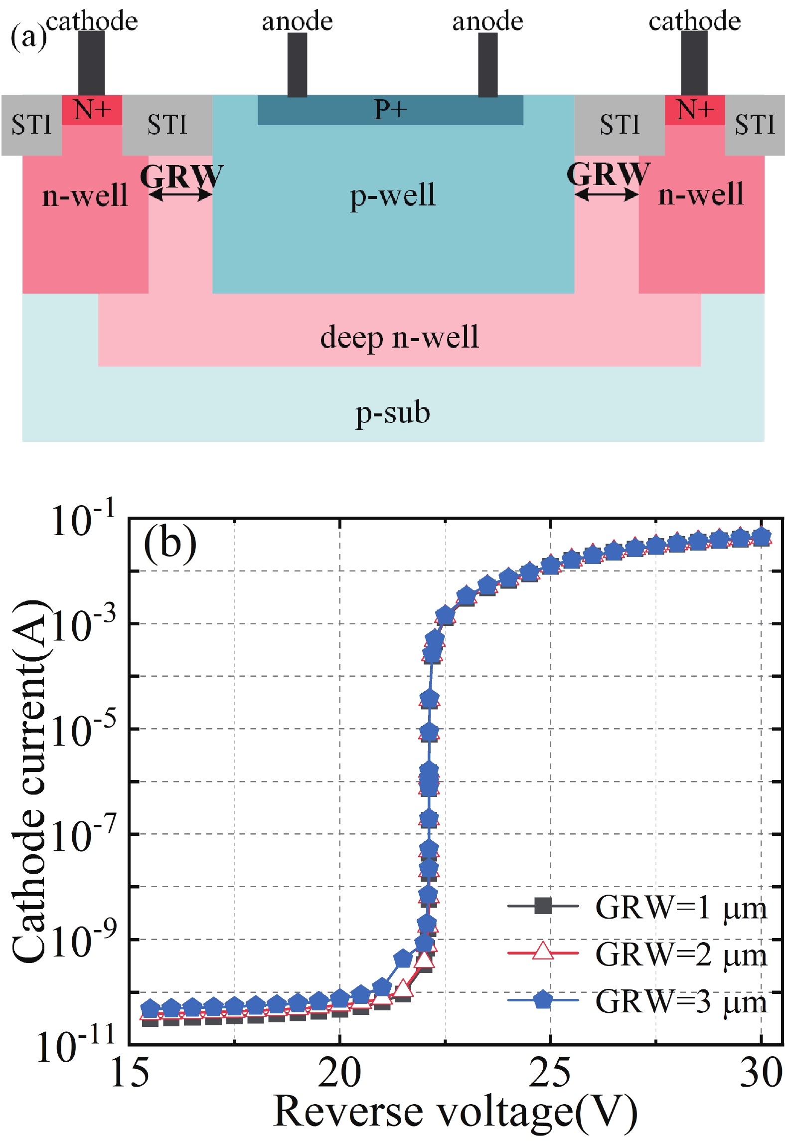
(Color online) (a) Schematic cross-section of the p-well/deep n-well SPAD. (b) TCAD simulation of the reverse I−V characteristics.
ARTICLES
Danlu Liu1, Ming Li1, Tang Xu1, Jie Dong1, Yuming Fang1, 2 and Yue Xu1, 2,
Corresponding author: Yue Xu, yuex@njupt.edu.cn
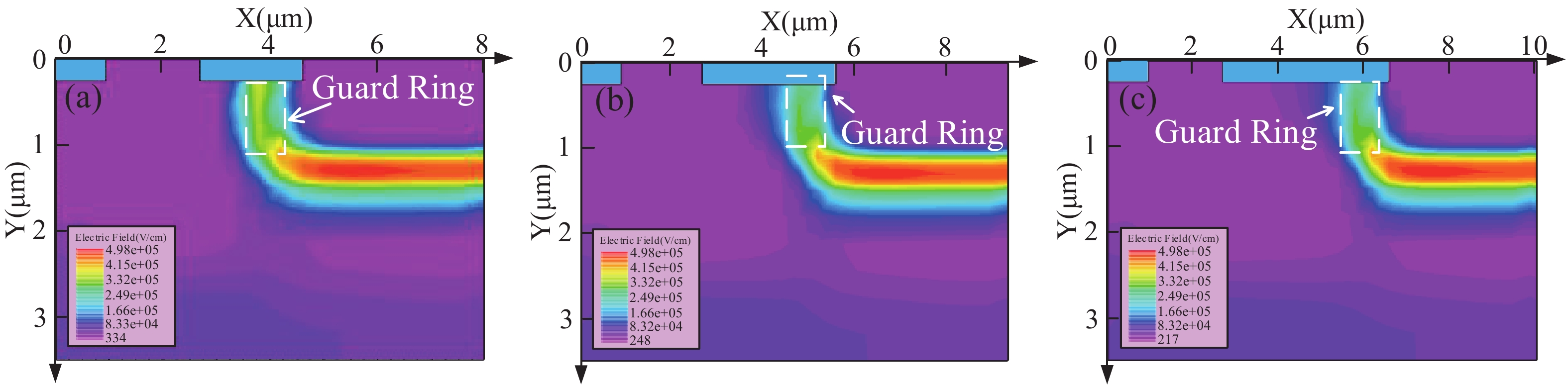
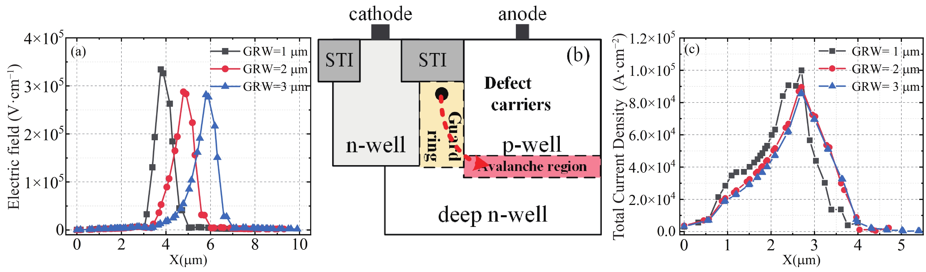
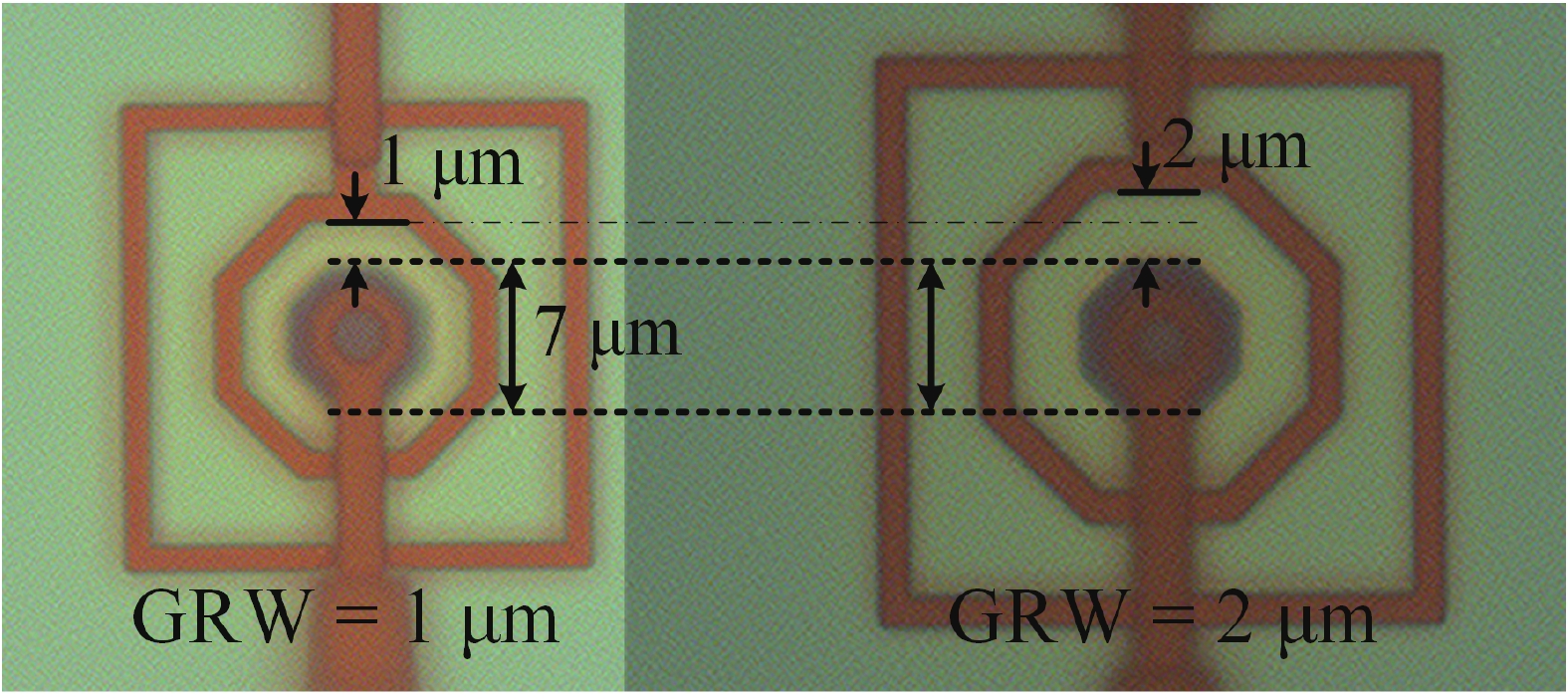
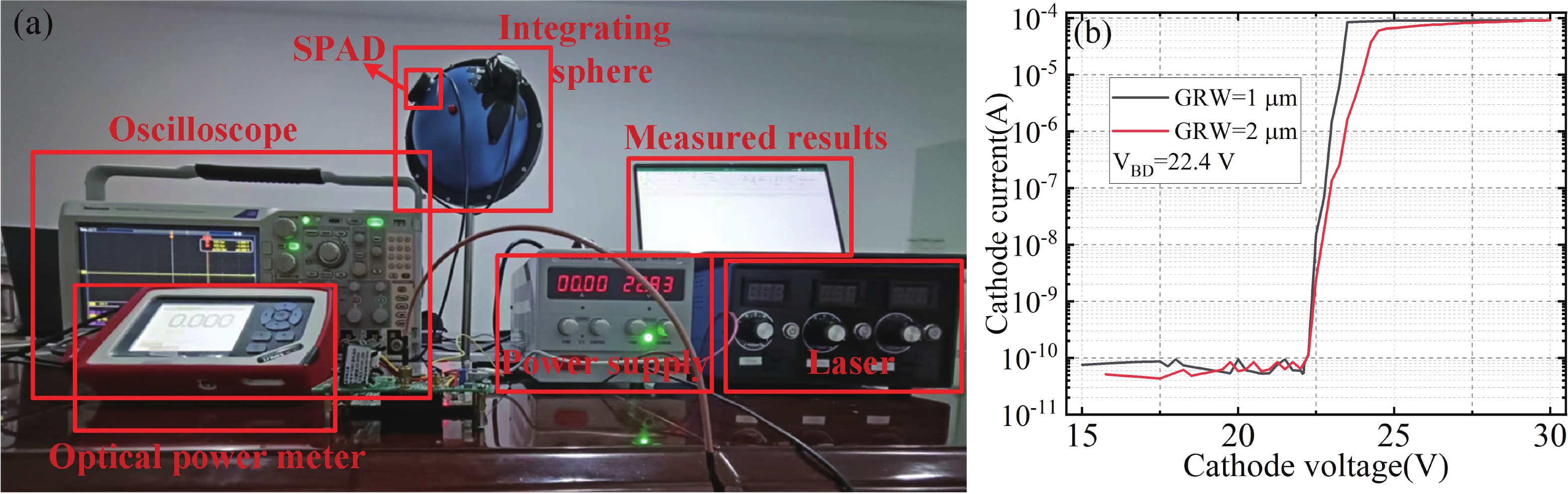
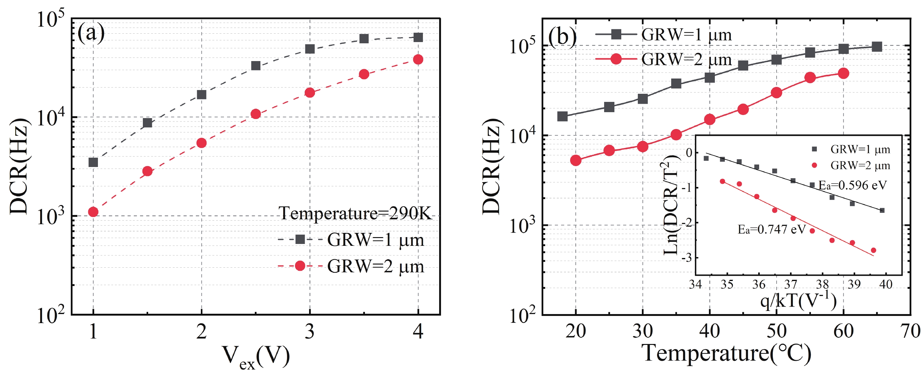
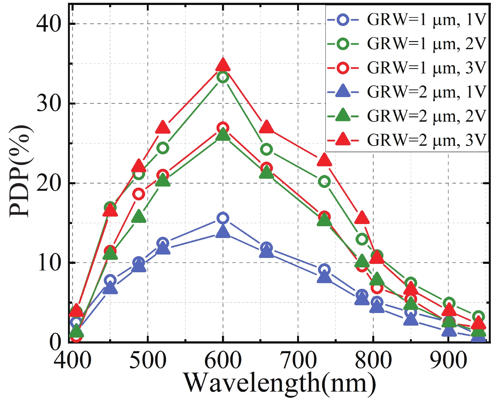
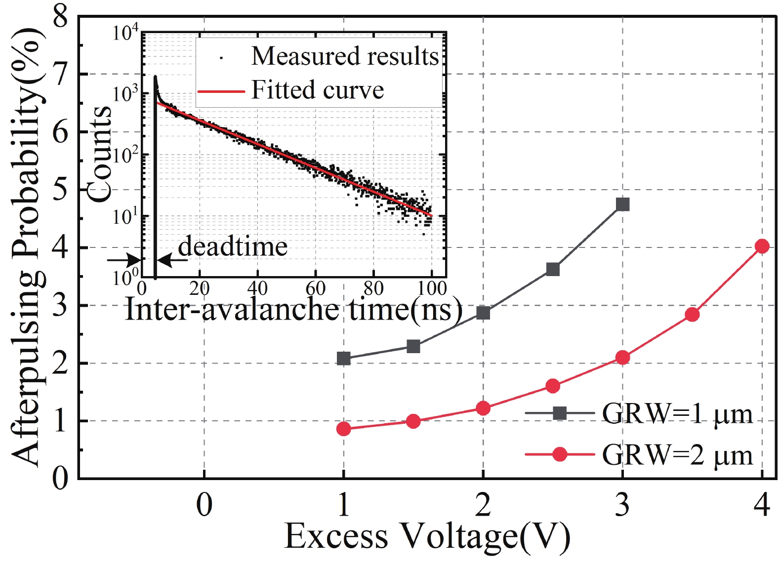
Abstract: The influence of the virtual guard ring width (GRW) on the performance of the p-well/deep n-well single-photon avalanche diode (SPAD) in a 180 nm standard CMOS process was investigated. TCAD simulation demonstrates that the electric field strength and current density in the guard ring are obviously enhanced when GRW is decreased to 1 μm. It is experimentally found that, compared with an SPAD with GRW = 2 μm, the dark count rate (DCR) and afterpulsing probability (AP) of the SPAD with GRW = 1 μm is significantly increased by 2.7 times and twofold, respectively, meanwhile, its photon detection probability (PDP) is saturated and hard to be promoted at over 2 V excess bias voltage. Although the fill factor (FF) can be enlarged by reducing GRW, the dark noise of devices is negatively affected due to the enhanced trap-assisted tunneling (TAT) effect in the 1 μm guard ring region. By comparison, the SPAD with GRW = 2 μm can achieve a better trade-off between the FF and noise performance. Our study provides a design guideline for guard rings to realize a low-noise SPAD for large-array applications.
Key words: single-photon avalanche diode (SPAD), virtual guard ring, dark count rate (DCR), photon detection probability (PDP), afterpulsing probability (AP)
| [1] |
Henderson R K, Johnston N, Chen H C, et al. A 192 × 128 time correlated single photon counting imager in 40nm CMOS technology. ESSCIRC 2018 - IEEE 44th European Solid State Circuits Conference (ESSCIRC), 2018, 54 doi: 10.1109/ESSCIRC.2018.8494330
|
| [2] |
Ma Z Q, Wu Z, Xu Y. Compact SPAD pixels with fast and accurate photon counting in the analog domain. J Semicond, 2021, 42, 052402 doi: 10.1088/1674-4926/42/5/052402
|
| [3] |
Dieguez A, Canals J, Franch N, et al. A compact analog histogramming SPAD-based CMOS chip for time-resolved fluorescence. IEEE Trans Biomed Circuits Syst, 2019, 13, 343 doi: 10.1109/TBCAS.2019.2892825
|
| [4] |
Moreno-García M, Xu H S, Gasparini L, et al. Low-noise single photon avalanche diodes in a 110nm CIS technology. 2018 48th European Solid-State Device Research Conference (ESSDERC), 2018, 94 doi: 10.1109/ESSDERC.2018.8486883
|
| [5] |
Veerappan C, Charbon E. A substrate isolated CMOS SPAD enabling wide spectral response and low electrical crosstalk. IEEE J Sel Top Quantum Electron, 2014, 20, 299 doi: 10.1109/JSTQE.2014.2318436
|
| [6] |
Vornicu I, López-Martínez J M, Bandi F N, et al. Design of high-efficiency SPADs for LiDAR applications in 110nm CIS technology. IEEE Sens J, 2021, 21, 4776 doi: 10.1109/JSEN.2020.3032106
|
| [7] |
Sanzaro M, Gattari P, Villa F, et al. Single-photon avalanche diodes in a 0.16 μm BCD technology with sharp timing response and red-enhanced sensitivity. IEEE J Sel Top Quantum Electron, 2017, 24, 1 doi: 10.1109/JSTQE.2017.2762464
|
| [8] |
Niclass C, Gersbach M, Henderson R, et al. A single photon avalanche diode implemented in 130-nm CMOS technology. IEEE J Sel Top Quantum Electron, 2007, 13, 863 doi: 10.1109/JSTQE.2007.903854
|
| [9] |
Lee M J, Sun P F, Pandraud G, et al. First near-ultraviolet- and blue-enhanced backside-illuminated single-photon avalanche diode based on standard SOI CMOS technology. IEEE J Sel Top Quantum Electron, 2019, 25, 1 doi: 10.1109/JSTQE.2019.2918930
|
| [10] |
Lu X, Law M K, Jiang Y, et al. A 4-μm diameter SPAD using less-doped N-well guard ring in baseline 65-nm CMOS. IEEE Trans Electron Devices, 2020, 67, 2223 doi: 10.1109/TED.2020.2982701
|
| [11] |
Liu Y, Liu M L, Ma R, et al. A wide spectral response single photon avalanche diode for backside-illumination in 55-nm CMOS process. IEEE Trans Electron Devices, 2022, 69, 5041 doi: 10.1109/TED.2022.3194488
|
| [12] |
Richardson J A, Webster E A G, Grant L A, et al. Scaleable single-photon avalanche diode structures in nanometer CMOS technology. IEEE Trans Electron Devices, 2011, 58, 2028 doi: 10.1109/TED.2011.2141138
|
| [13] |
Jiang W, Chalich Y, Scott R, et al. Time-gated and multi-junction SPADs in standard 65 nm CMOS technology. IEEE Sens J, 2021, 21, 12092 doi: 10.1109/JSEN.2021.3063319
|
| [14] |
Sicre M, Agnew M, Buj C, et al. Dark count rate in single-photon avalanche diodes: Characterization and modeling study. ESSDERC 2021-IEEE 51st European Solid-State Device Research Conference (ESSDERC), 2021, 143 doi: 10.1109/ESSDERC53440.2021.9631797
|
| [15] |
Kindt W, Zeijl H. Modelling and fabrication of Geiger mode avalanche photodiodes. IEEE Trans Nucl Sci, 1998, 45, 715 doi: 10.1109/23.682621
|
| [16] |
Hurkx G A M, Klaassen D, Knuvers M. A new recombination model for device simulation including tunneling. IEEE Trans Electron Devices, 1992, 39, 331 doi: 10.1109/16.121690
|
| [17] |
Vornicu I, Bandi F, Carmona-Galán R, et al. Low-noise and high-efficiency near-IR SPADs in 110nm CIS technology. ESSDERC 2019-49th European Solid-State Device Research Conference (ESSDERC), 2019, 250 doi: 10.1109/ESSDERC.2019.8901757
|
| [18] |
Palubiak D P, Deen M J. CMOS SPADs: Design issues and research challenges for detectors, circuits, and arrays. IEEE J Sel Top Quantum Electron, 2014, 20, 409 doi: 10.1109/JSTQE.2014.2344034
|
| [19] |
Webster E A, Grant L A, Henderson R K. A high-performance single-photon avalanche diode in 130-nm CMOS imaging technology. IEEE Electron Device Lett, 2012, 33, 1589 doi: 10.1109/LED.2012.2214760
|
| [20] |
Xu Y, Xiang P, Xie X P, et al. A new modeling and simulation method for important statistical performance prediction of single photon avalanche diode detectors. Semicond Sci Technol, 2016, 31, 065024 doi: 10.1088/0268-1242/31/6/065024
|
| [21] |
Mandai S, Fishburn M W, Maruyama Y, et al. A wide spectral range single-photon avalanche diode fabricated in an advanced 180 nm CMOS technology. Opt Express, 2012, 20, 5849 doi: 10.1364/OE.20.005849
|


Article views: 869 Times PDF downloads: 131 Times Cited by: 0 Times
Received: 31 March 2022 Revised: 14 June 2023 Online: Accepted Manuscript: 28 August 2023Uncorrected proof: 20 October 2023Published: 10 November 2023
| Citation: |
Danlu Liu, Ming Li, Tang Xu, Jie Dong, Yuming Fang, Yue Xu. Study of the influence of virtual guard ring width on the performance of SPAD detectors in 180 nm standard CMOS technology[J]. Journal of Semiconductors, 2023, 44(11): 114102. doi: 10.1088/1674-4926/44/11/114102
****
D L Liu, M Li, T Xu, J Dong, Y M Fang, Y Xu. Study of the influence of virtual guard ring width on the performance of SPAD detectors in 180 nm standard CMOS technology[J]. J. Semicond, 2023, 44(11): 114102. doi: 10.1088/1674-4926/44/11/114102

|
 Danlu Liu:received a bachelor’s degree in electronic science and technology from Nanjing University of Posts and Telecommunications, Nanjing, China, in 2021. She is currently pursuing a master’s degree with the Nanjing University of Posts and Telecommunications, Nanjing, China
 Yue Xu:received a PhD degree in microelectronics and solid-state electronics from Nanjing University, China, in 2012. He is currently a professor with the Nanjing University of Posts and Telecommunications, Nanjing, China. His main research interests include the CMOS detector, analog-integrated circuit design and device reliability
| [1] |
Henderson R K, Johnston N, Chen H C, et al. A 192 × 128 time correlated single photon counting imager in 40nm CMOS technology. ESSCIRC 2018 - IEEE 44th European Solid State Circuits Conference (ESSCIRC), 2018, 54 doi: 10.1109/ESSCIRC.2018.8494330
|
| [2] |
Ma Z Q, Wu Z, Xu Y. Compact SPAD pixels with fast and accurate photon counting in the analog domain. J Semicond, 2021, 42, 052402 doi: 10.1088/1674-4926/42/5/052402
|
| [3] |
Dieguez A, Canals J, Franch N, et al. A compact analog histogramming SPAD-based CMOS chip for time-resolved fluorescence. IEEE Trans Biomed Circuits Syst, 2019, 13, 343 doi: 10.1109/TBCAS.2019.2892825
|
| [4] |
Moreno-García M, Xu H S, Gasparini L, et al. Low-noise single photon avalanche diodes in a 110nm CIS technology. 2018 48th European Solid-State Device Research Conference (ESSDERC), 2018, 94 doi: 10.1109/ESSDERC.2018.8486883
|
| [5] |
Veerappan C, Charbon E. A substrate isolated CMOS SPAD enabling wide spectral response and low electrical crosstalk. IEEE J Sel Top Quantum Electron, 2014, 20, 299 doi: 10.1109/JSTQE.2014.2318436
|
| [6] |
Vornicu I, López-Martínez J M, Bandi F N, et al. Design of high-efficiency SPADs for LiDAR applications in 110nm CIS technology. IEEE Sens J, 2021, 21, 4776 doi: 10.1109/JSEN.2020.3032106
|
| [7] |
Sanzaro M, Gattari P, Villa F, et al. Single-photon avalanche diodes in a 0.16 μm BCD technology with sharp timing response and red-enhanced sensitivity. IEEE J Sel Top Quantum Electron, 2017, 24, 1 doi: 10.1109/JSTQE.2017.2762464
|
| [8] |
Niclass C, Gersbach M, Henderson R, et al. A single photon avalanche diode implemented in 130-nm CMOS technology. IEEE J Sel Top Quantum Electron, 2007, 13, 863 doi: 10.1109/JSTQE.2007.903854
|
| [9] |
Lee M J, Sun P F, Pandraud G, et al. First near-ultraviolet- and blue-enhanced backside-illuminated single-photon avalanche diode based on standard SOI CMOS technology. IEEE J Sel Top Quantum Electron, 2019, 25, 1 doi: 10.1109/JSTQE.2019.2918930
|
| [10] |
Lu X, Law M K, Jiang Y, et al. A 4-μm diameter SPAD using less-doped N-well guard ring in baseline 65-nm CMOS. IEEE Trans Electron Devices, 2020, 67, 2223 doi: 10.1109/TED.2020.2982701
|
| [11] |
Liu Y, Liu M L, Ma R, et al. A wide spectral response single photon avalanche diode for backside-illumination in 55-nm CMOS process. IEEE Trans Electron Devices, 2022, 69, 5041 doi: 10.1109/TED.2022.3194488
|
| [12] |
Richardson J A, Webster E A G, Grant L A, et al. Scaleable single-photon avalanche diode structures in nanometer CMOS technology. IEEE Trans Electron Devices, 2011, 58, 2028 doi: 10.1109/TED.2011.2141138
|
| [13] |
Jiang W, Chalich Y, Scott R, et al. Time-gated and multi-junction SPADs in standard 65 nm CMOS technology. IEEE Sens J, 2021, 21, 12092 doi: 10.1109/JSEN.2021.3063319
|
| [14] |
Sicre M, Agnew M, Buj C, et al. Dark count rate in single-photon avalanche diodes: Characterization and modeling study. ESSDERC 2021-IEEE 51st European Solid-State Device Research Conference (ESSDERC), 2021, 143 doi: 10.1109/ESSDERC53440.2021.9631797
|
| [15] |
Kindt W, Zeijl H. Modelling and fabrication of Geiger mode avalanche photodiodes. IEEE Trans Nucl Sci, 1998, 45, 715 doi: 10.1109/23.682621
|
| [16] |
Hurkx G A M, Klaassen D, Knuvers M. A new recombination model for device simulation including tunneling. IEEE Trans Electron Devices, 1992, 39, 331 doi: 10.1109/16.121690
|
| [17] |
Vornicu I, Bandi F, Carmona-Galán R, et al. Low-noise and high-efficiency near-IR SPADs in 110nm CIS technology. ESSDERC 2019-49th European Solid-State Device Research Conference (ESSDERC), 2019, 250 doi: 10.1109/ESSDERC.2019.8901757
|
| [18] |
Palubiak D P, Deen M J. CMOS SPADs: Design issues and research challenges for detectors, circuits, and arrays. IEEE J Sel Top Quantum Electron, 2014, 20, 409 doi: 10.1109/JSTQE.2014.2344034
|
| [19] |
Webster E A, Grant L A, Henderson R K. A high-performance single-photon avalanche diode in 130-nm CMOS imaging technology. IEEE Electron Device Lett, 2012, 33, 1589 doi: 10.1109/LED.2012.2214760
|
| [20] |
Xu Y, Xiang P, Xie X P, et al. A new modeling and simulation method for important statistical performance prediction of single photon avalanche diode detectors. Semicond Sci Technol, 2016, 31, 065024 doi: 10.1088/0268-1242/31/6/065024
|
| [21] |
Mandai S, Fishburn M W, Maruyama Y, et al. A wide spectral range single-photon avalanche diode fabricated in an advanced 180 nm CMOS technology. Opt Express, 2012, 20, 5849 doi: 10.1364/OE.20.005849
|

 WeChat ID
Journal of Semiconductors © 2017 All Rights Reserved 京ICP备05085259号-2

 DownLoad:

