


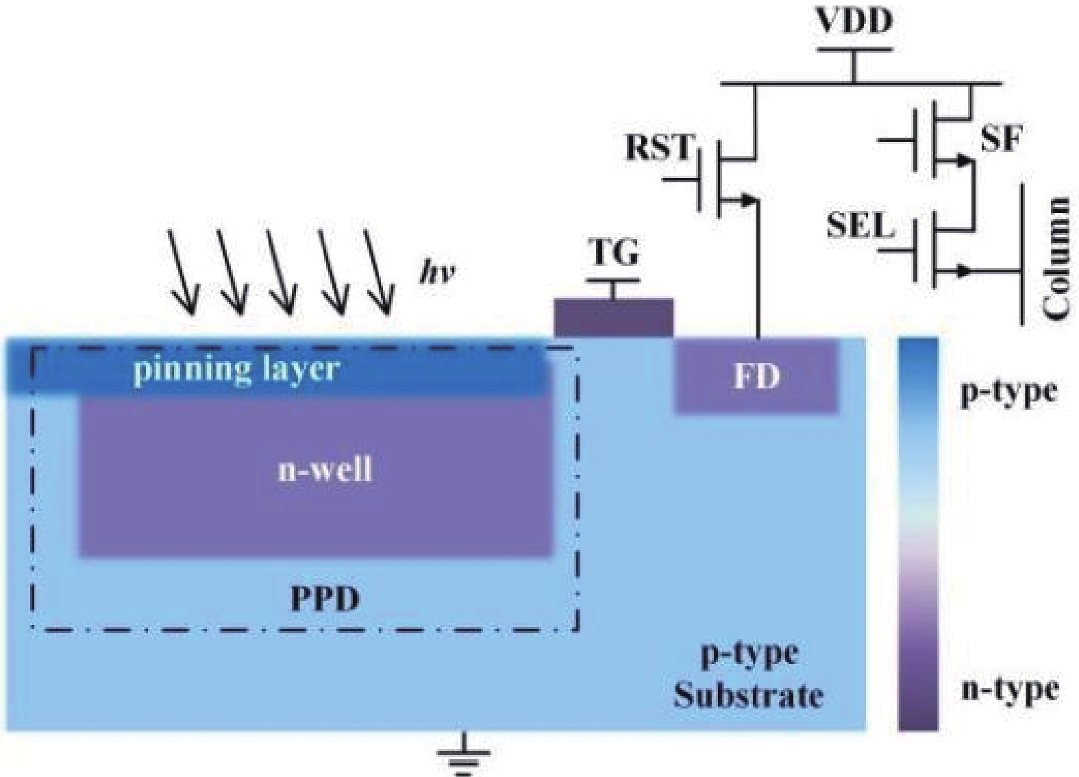
Fig. 1.
(Color online) Four-transistor pixel structure of the PPD CIS.
ARTICLES
Xi Lu1, §, Changju Liu2, 3, §, Pinyuan Zhao1, Yu Zhang1, , Bei Li3, Zhenzhen Zhang1 and Jiangtao Xu2,
Corresponding author: Yu Zhang, zy2009@hdu.edu.cn; Jiangtao Xu, xujiangtao@tju.edu.cn
Abstract: CMOS image sensors produced by the existing CMOS manufacturing process usually have difficulty achieving complete charge transfer owing to the introduction of potential barriers or Si/SiO2 interface state traps in the charge transfer path, which reduces the charge transfer efficiency and image quality. Until now, scholars have only considered mechanisms that limit charge transfer from the perspectives of potential barriers and spill back effect under high illumination condition. However, the existing models have thus far ignored the charge transfer limitation due to Si/SiO2 interface state traps in the transfer gate channel, particularly under low illumination. Therefore, this paper proposes, for the first time, an analytical model for quantifying the incomplete charge transfer caused by Si/SiO2 interface state traps in the transfer gate channel under low illumination. This model can predict the variation rules of the number of untransferred charges and charge transfer efficiency when the trap energy level follows Gaussian distribution, exponential distribution and measured distribution. The model was verified with technology computer-aided design simulations, and the results showed that the simulation results exhibit the consistency with the proposed model.
Key words: CMOS image sensor, charge transfer, interface state traps
| [1] |
Fossum E R, Hondongwa D B. A review of the pinned photodiode for CCD and CMOS image sensors. IEEE J Electron Devices Soc, 2014, 2, 33 doi: 10.1109/JEDS.2014.2306412
|
| [2] |
Takayanagi I, Kuroda R. HDR CMOS image sensors for automotive applications. IEEE Trans Electron Devices, 2022, 69, 2815 doi: 10.1109/TED.2022.3164370
|
| [3] |
Liu B K, Li Y D, Wen L, et al. Displacement damage effects in backside illuminated CMOS image sensors. IEEE Trans Electron Devices, 2022, 69, 2907 doi: 10.1109/TED.2021.3124991
|
| [4] |
Lee Y S, Kim H J. High-speed multilevel binary imaging CMOS image sensor for object feature extraction. IEEE Sens J, 2022, 22, 15934 doi: 10.1109/JSEN.2022.3189653
|
| [5] |
Marcelot O, Panglosse A, Martin-Gonthier P, et al. TCAD calibration at cryogenic temperatures for CMOS image sensor simulations. IEEE Trans Electron Devices, 2022, 69, 6188 doi: 10.1109/TED.2022.3207120
|
| [6] |
Rizzolo S, Goiffon V, Estribeau M, et al. Influence of pixel design on charge transfer performances in CMOS image sensors. IEEE Trans Electron Devices, 2018, 65, 1048 doi: 10.1109/TED.2018.2790443
|
| [7] |
Han L Q, Yao S Y, Theuwissen A J P. A charge transfer model for CMOS image sensors. IEEE Trans Electron Devices, 2016, 63, 32 doi: 10.1109/TED.2015.2451593
|
| [8] |
Fossum E R. Charge transfer noise and lag in CMOS active pixel sensors. IEEE Workshop CCD’s Adv. Image Sensors, 2003, 11
|
| [9] |
Han L Q, Yao S Y, Xu J T, et al. Analysis of incomplete charge transfer effects in a CMOS image sensor. J Semicond, 2013, 34, 054009 doi: 10.1088/1674-4926/34/5/054009
|
| [10] |
Capoccia R, Boukhayma A, Jazaeri F, et al. Compact modeling of charge transfer in pinned photodiodes for CMOS image sensors. IEEE Trans Electron Devices, 2018, 66, 160 doi: 10.1109/TED.2018.2875946
|
| [11] |
Yang C, Peng G L, Mao W, et al. Novel CMOS image sensor pixel to improve charge transfer speed and efficiency by overlapping gate and temporary storage diffusing node. Chin Phys B, 2021, 30, 018502 doi: 10.1088/1674-1056/abc53f
|
| [12] |
Wang X Y, Gao Y Q, Gao Z Y, et al. Charge transfer potential barrier model of a pinned photodiode in CMOS image sensors. IEEE Sens J, 2022, 22, 4036 doi: 10.1109/JSEN.2021.3139091
|
| [13] |
Khan U, Sarkar M. Analysis of charge transfer potential barrier in pinned photodiode of CMOS image sensors. IEEE Trans Electron Devices, 2021, 68, 2770 doi: 10.1109/TED.2021.3071331
|
| [14] |
Liu L, Guo Y, Li B K, et al. Analytical modeling of potential barrier for charge transfer in pinned photodiode CMOS image sensors. IEEE Trans Electron Devices, 2022, 69, 5637 doi: 10.1109/TED.2022.3200636
|
| [15] |
Hu C Z, Zhang B, Xin Y Z, et al. Analytical modeling of charge behavior in pinned photodiode for CMOS image sensors. IEEE Sens J, 2023, 23, 14295 doi: 10.1109/JSEN.2023.3278307
|
| [16] |
Xu J T, Wang R S, Han L Q, et al. Analysis and modeling of spill back effect in high illumination CMOS image sensors. IEEE Sens J, 2020, 20, 3024 doi: 10.1109/JSEN.2019.2956594
|
| [17] |
Xu Y. Fundamental characteristics of a pinned photodiode CMOS pixel. Ph. D. dissertation, Dept. Microelectron. Comput. Eng., Delft Univ. Technol., Delft, the Netherlands, 2015
|
| [18] |
Fowler B , Liu X. Charge transfer noise in image sensors. International Image Sensor Workshop (IISW), 2007, 2
|
| [19] |
Bonjour L E, Blanc N, Kayal M. Experimental analysis of lag sources in pinned photodiodes. IEEE Electron Device Lett, 2012, 33, 1735 doi: 10.1109/LED.2012.2217474
|
| [20] |
Khan U, Sarkar M. Dynamic capacitance model of a pinned photodiode in CMOS image sensors. IEEE Trans Electron Devices, 2018, 65, 2892 doi: 10.1109/TED.2018.2831719
|
| [21] |
Liu E, Zhu B, Luo J. The physics of semiconductors. Beijing: House of Electronics Industry, 2011
|
| [22] |
Mohsen A M, McGill T C, Daimon Y, et al. The influence of interface states on incomplete charge transfer in overlapping gate charge-coupled devices. IEEE J Solid-State Circuits, 1973, 8, 125 doi: 10.1109/JSSC.1973.1050361
|
| [23] |
Han L Q, Xu J T. Long exposure time noise in pinned photodiode CMOS image sensors. IEEE Electron Device Lett, 2018, 39, 979 doi: 10.1109/LED.2018.2839711
|
| [24] |
Xia C Y, Zhang Y, Lu X M, et al. Dynamic model of FWC dependent on the energy-level distribution of interface-state traps in pinned photodiodes. IEEE Trans Electron Devices, 2021, 68, 1682 doi: 10.1109/TED.2021.3056019
|
| [25] |
Ayobi A, Mirnia S N. Influence of Gaussian disorder and exponential traps on charge carriers transport and recombination in single layer polymer light-emitting diodes based on PFO as emitting layer. Opt Quantum Electron, 2019, 51, 1 doi: 10.1007/s11082-018-1712-9
|
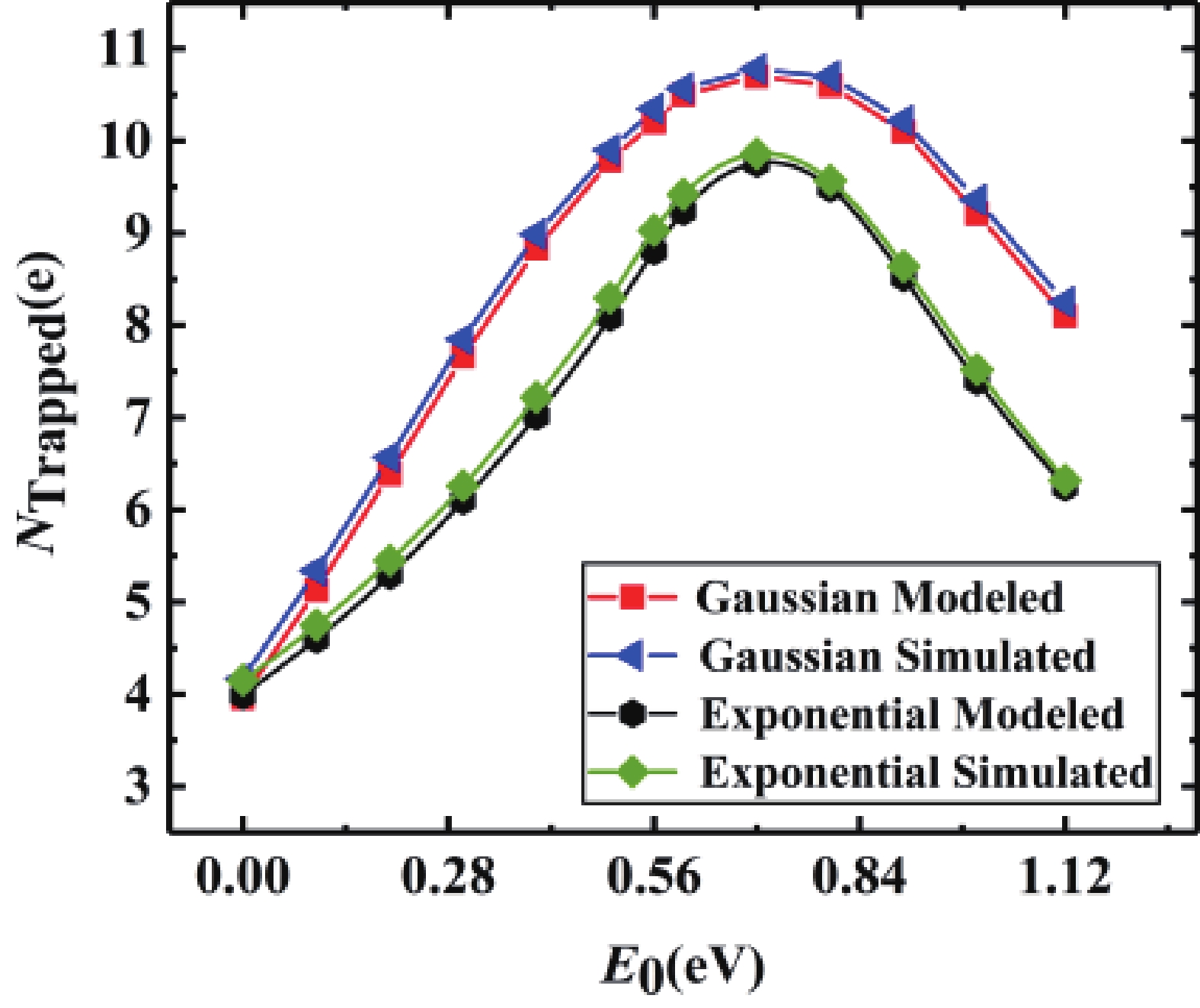
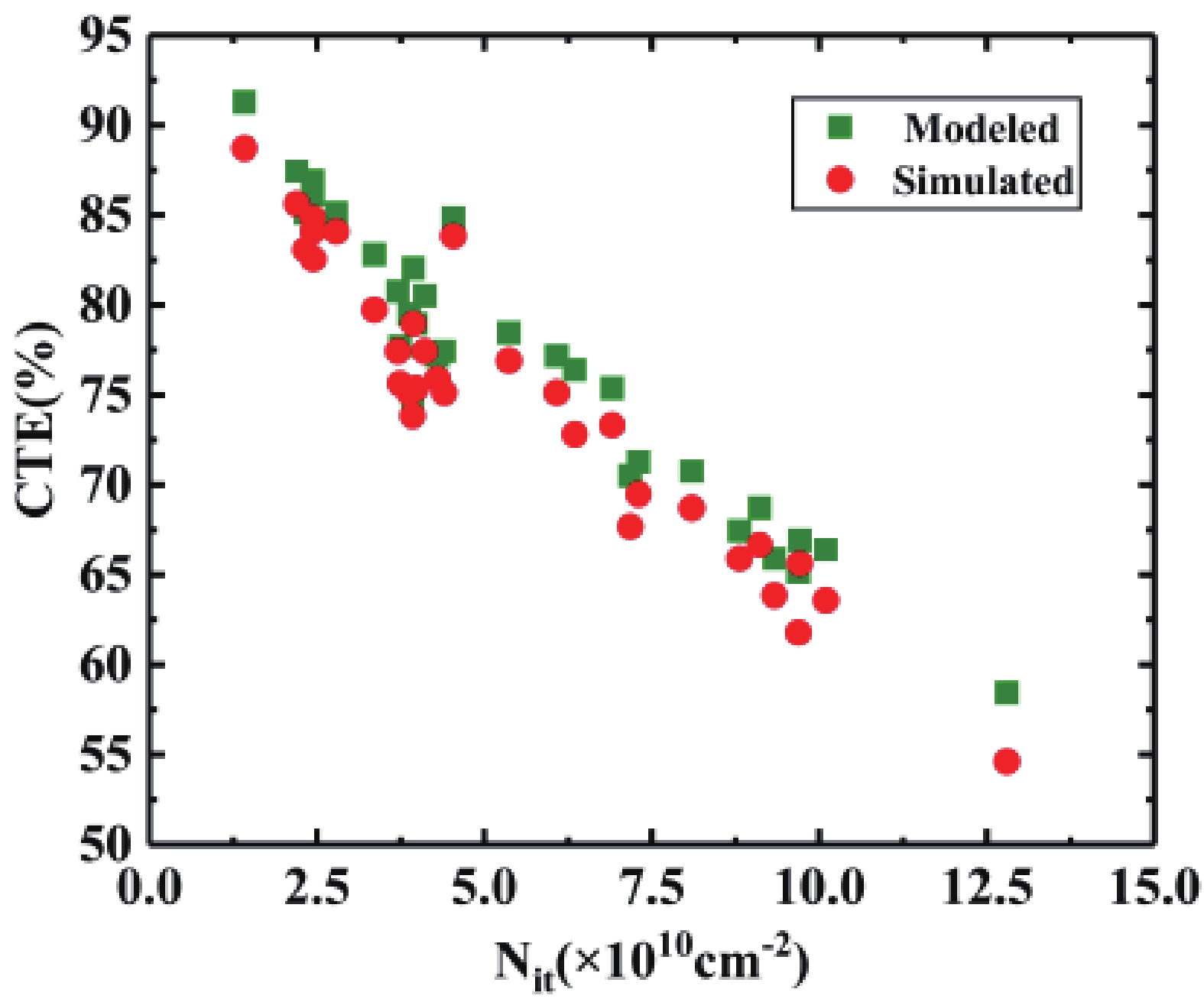
Table 1. Parameters of the mathematical model.
| Parameters | Description | Value |
| NA | Doping concentration of the p-type substrate | 1015 cm-3 |
| ND | Doping concentration of the n-well | 1017 cm-3 |
| NA+ | Doping concentration of the top pinning layer | 1020 cm-3 |
| NC | Effective state density of conduction band | 2.8 × 1019 cm-3 |
| vt | Thermal velocity | 107 cm/s |
| q | Unit charge | 1.6 × 10⁻¹⁹ C |
| K | Boltzmann constant | 1.38 × 10⁻²³ J/K |
| T | Temperature | 300 K |
| LTG | Length of the TG | 0.7 μm |
| LPPD | Length of the pinned photodiode | 2 μm |
| ATG | Area of the TG | 0.7 μm2 |
| tfall | Time required for the TG to drop from VTG-High to VTG-Low | 1 ns |
| Nmax | The coefficient of Gaussian and exponential distribution | 5 ×1010 cm−2·eV-1 |
| n | Electron density of Si semiconductor | 1015 cm-3 |
| $ {\text{σ}}_{\text{n}} $ | Electron capture cross-section | 10-15 cm-2 |
 DownLoad: CSV
| [1] |
Fossum E R, Hondongwa D B. A review of the pinned photodiode for CCD and CMOS image sensors. IEEE J Electron Devices Soc, 2014, 2, 33 doi: 10.1109/JEDS.2014.2306412
|
| [2] |
Takayanagi I, Kuroda R. HDR CMOS image sensors for automotive applications. IEEE Trans Electron Devices, 2022, 69, 2815 doi: 10.1109/TED.2022.3164370
|
| [3] |
Liu B K, Li Y D, Wen L, et al. Displacement damage effects in backside illuminated CMOS image sensors. IEEE Trans Electron Devices, 2022, 69, 2907 doi: 10.1109/TED.2021.3124991
|
| [4] |
Lee Y S, Kim H J. High-speed multilevel binary imaging CMOS image sensor for object feature extraction. IEEE Sens J, 2022, 22, 15934 doi: 10.1109/JSEN.2022.3189653
|
| [5] |
Marcelot O, Panglosse A, Martin-Gonthier P, et al. TCAD calibration at cryogenic temperatures for CMOS image sensor simulations. IEEE Trans Electron Devices, 2022, 69, 6188 doi: 10.1109/TED.2022.3207120
|
| [6] |
Rizzolo S, Goiffon V, Estribeau M, et al. Influence of pixel design on charge transfer performances in CMOS image sensors. IEEE Trans Electron Devices, 2018, 65, 1048 doi: 10.1109/TED.2018.2790443
|
| [7] |
Han L Q, Yao S Y, Theuwissen A J P. A charge transfer model for CMOS image sensors. IEEE Trans Electron Devices, 2016, 63, 32 doi: 10.1109/TED.2015.2451593
|
| [8] |
Fossum E R. Charge transfer noise and lag in CMOS active pixel sensors. IEEE Workshop CCD’s Adv. Image Sensors, 2003, 11
|
| [9] |
Han L Q, Yao S Y, Xu J T, et al. Analysis of incomplete charge transfer effects in a CMOS image sensor. J Semicond, 2013, 34, 054009 doi: 10.1088/1674-4926/34/5/054009
|
| [10] |
Capoccia R, Boukhayma A, Jazaeri F, et al. Compact modeling of charge transfer in pinned photodiodes for CMOS image sensors. IEEE Trans Electron Devices, 2018, 66, 160 doi: 10.1109/TED.2018.2875946
|
| [11] |
Yang C, Peng G L, Mao W, et al. Novel CMOS image sensor pixel to improve charge transfer speed and efficiency by overlapping gate and temporary storage diffusing node. Chin Phys B, 2021, 30, 018502 doi: 10.1088/1674-1056/abc53f
|
| [12] |
Wang X Y, Gao Y Q, Gao Z Y, et al. Charge transfer potential barrier model of a pinned photodiode in CMOS image sensors. IEEE Sens J, 2022, 22, 4036 doi: 10.1109/JSEN.2021.3139091
|
| [13] |
Khan U, Sarkar M. Analysis of charge transfer potential barrier in pinned photodiode of CMOS image sensors. IEEE Trans Electron Devices, 2021, 68, 2770 doi: 10.1109/TED.2021.3071331
|
| [14] |
Liu L, Guo Y, Li B K, et al. Analytical modeling of potential barrier for charge transfer in pinned photodiode CMOS image sensors. IEEE Trans Electron Devices, 2022, 69, 5637 doi: 10.1109/TED.2022.3200636
|
| [15] |
Hu C Z, Zhang B, Xin Y Z, et al. Analytical modeling of charge behavior in pinned photodiode for CMOS image sensors. IEEE Sens J, 2023, 23, 14295 doi: 10.1109/JSEN.2023.3278307
|
| [16] |
Xu J T, Wang R S, Han L Q, et al. Analysis and modeling of spill back effect in high illumination CMOS image sensors. IEEE Sens J, 2020, 20, 3024 doi: 10.1109/JSEN.2019.2956594
|
| [17] |
Xu Y. Fundamental characteristics of a pinned photodiode CMOS pixel. Ph. D. dissertation, Dept. Microelectron. Comput. Eng., Delft Univ. Technol., Delft, the Netherlands, 2015
|
| [18] |
Fowler B , Liu X. Charge transfer noise in image sensors. International Image Sensor Workshop (IISW), 2007, 2
|
| [19] |
Bonjour L E, Blanc N, Kayal M. Experimental analysis of lag sources in pinned photodiodes. IEEE Electron Device Lett, 2012, 33, 1735 doi: 10.1109/LED.2012.2217474
|
| [20] |
Khan U, Sarkar M. Dynamic capacitance model of a pinned photodiode in CMOS image sensors. IEEE Trans Electron Devices, 2018, 65, 2892 doi: 10.1109/TED.2018.2831719
|
| [21] |
Liu E, Zhu B, Luo J. The physics of semiconductors. Beijing: House of Electronics Industry, 2011
|
| [22] |
Mohsen A M, McGill T C, Daimon Y, et al. The influence of interface states on incomplete charge transfer in overlapping gate charge-coupled devices. IEEE J Solid-State Circuits, 1973, 8, 125 doi: 10.1109/JSSC.1973.1050361
|
| [23] |
Han L Q, Xu J T. Long exposure time noise in pinned photodiode CMOS image sensors. IEEE Electron Device Lett, 2018, 39, 979 doi: 10.1109/LED.2018.2839711
|
| [24] |
Xia C Y, Zhang Y, Lu X M, et al. Dynamic model of FWC dependent on the energy-level distribution of interface-state traps in pinned photodiodes. IEEE Trans Electron Devices, 2021, 68, 1682 doi: 10.1109/TED.2021.3056019
|
| [25] |
Ayobi A, Mirnia S N. Influence of Gaussian disorder and exponential traps on charge carriers transport and recombination in single layer polymer light-emitting diodes based on PFO as emitting layer. Opt Quantum Electron, 2019, 51, 1 doi: 10.1007/s11082-018-1712-9
|


Article views: 863 Times PDF downloads: 108 Times Cited by: 0 Times
Received: 16 August 2023 Revised: 18 September 2023 Online: Accepted Manuscript: 01 November 2023Uncorrected proof: 08 November 2023Published: 10 November 2023
| Citation: |
Xi Lu, Changju Liu, Pinyuan Zhao, Yu Zhang, Bei Li, Zhenzhen Zhang, Jiangtao Xu. Incomplete charge transfer in CMOS image sensor caused by Si/SiO2 interface states in the TG channel[J]. Journal of Semiconductors, 2023, 44(11): 114104. doi: 10.1088/1674-4926/44/11/114104
****
X Lu, C J Liu, P Y Zhao, Y Zhang, B Li, Z Z Zhang, J T Xu. Incomplete charge transfer in CMOS image sensor caused by Si/SiO2 interface states in the TG channel[J]. J. Semicond, 2023, 44(11): 114104. doi: 10.1088/1674-4926/44/11/114104

|
 Xi Lu:received the B.E. degree from the School of Electrical Engineering and Automation, Tianjin Polytechnic University, Tianjin, China, in 2020. She is currently pursuing the master’s degree with the School of Electronic Information, Hangzhou Dianzi University, Hangzhou, China. Her current research interests include CMOS image sensor and pixel design
 Changju Liu:is from Chonqing Optoelectronics Research Institute, Chongqing, China, he received the M.S. degree in 2007 from University of Electronic Science and Technology of China. His research activities are focused on CCD/CMOS image sensor and optoelectronic integrated devices
 Pinyuan Zhao:received the B.E. degree from the School of Electronic Information, Anhui University of Technology, Anhui, China, in 2021. She is currently pursuing the master’s degree with the School of Electronic Information, Hangzhou Dianzi University, Hangzhou, China. Her current research interests include CMOS image sensor design especially on pixel design
 Yu Zhang:received the M.S. degree in circuit and system from Tianjin University, Tianjin, China, in 2006 and the Ph.D. degree in Microelectronics and solid state electronics from Tianjin University, Tianjin, China, in 2009. Since July 2009, she has been with the School of Electronics and Information, Hangzhou Dianzi University, and currently is full professor of this university. Her research interests are noise model and VLSI realization of CMOS image sensor
 Bei Li:received his bachelor's degree in 2002 from NorthWest University. He is a senior engineer of Chonqing Optoelectronics Research Institute, Chongqing, China. His research focuses on wafer test
 Zhenzhen Zhang:received the B.E. degree from the School of Electronic Information, Xi'an Shiyou University of Technology, Xi'an, China, in 2020. She is currently pursuing the master’s degree with the School of Electronic Information, Hangzhou Dianzi University, Hangzhou, China. Her current research interests include signal processing
 Jiangtao Xu:received the B.E. degree from Tianjin University in 2001, the M.S. and Ph.D. degrees from the School of Electronic Information and Engineering, Tianjin University, in 2004 and 2007, respectively. From 2007 to 2010, he was a Lecturer. From 2010 to 2018, he was an Associate Professor with Tianjin University. Since 2018, he has been a full Professor with the School of Microelectronics. His research interests are in CMOS image sensor chip and system
| [1] |
Fossum E R, Hondongwa D B. A review of the pinned photodiode for CCD and CMOS image sensors. IEEE J Electron Devices Soc, 2014, 2, 33 doi: 10.1109/JEDS.2014.2306412
|
| [2] |
Takayanagi I, Kuroda R. HDR CMOS image sensors for automotive applications. IEEE Trans Electron Devices, 2022, 69, 2815 doi: 10.1109/TED.2022.3164370
|
| [3] |
Liu B K, Li Y D, Wen L, et al. Displacement damage effects in backside illuminated CMOS image sensors. IEEE Trans Electron Devices, 2022, 69, 2907 doi: 10.1109/TED.2021.3124991
|
| [4] |
Lee Y S, Kim H J. High-speed multilevel binary imaging CMOS image sensor for object feature extraction. IEEE Sens J, 2022, 22, 15934 doi: 10.1109/JSEN.2022.3189653
|
| [5] |
Marcelot O, Panglosse A, Martin-Gonthier P, et al. TCAD calibration at cryogenic temperatures for CMOS image sensor simulations. IEEE Trans Electron Devices, 2022, 69, 6188 doi: 10.1109/TED.2022.3207120
|
| [6] |
Rizzolo S, Goiffon V, Estribeau M, et al. Influence of pixel design on charge transfer performances in CMOS image sensors. IEEE Trans Electron Devices, 2018, 65, 1048 doi: 10.1109/TED.2018.2790443
|
| [7] |
Han L Q, Yao S Y, Theuwissen A J P. A charge transfer model for CMOS image sensors. IEEE Trans Electron Devices, 2016, 63, 32 doi: 10.1109/TED.2015.2451593
|
| [8] |
Fossum E R. Charge transfer noise and lag in CMOS active pixel sensors. IEEE Workshop CCD’s Adv. Image Sensors, 2003, 11
|
| [9] |
Han L Q, Yao S Y, Xu J T, et al. Analysis of incomplete charge transfer effects in a CMOS image sensor. J Semicond, 2013, 34, 054009 doi: 10.1088/1674-4926/34/5/054009
|
| [10] |
Capoccia R, Boukhayma A, Jazaeri F, et al. Compact modeling of charge transfer in pinned photodiodes for CMOS image sensors. IEEE Trans Electron Devices, 2018, 66, 160 doi: 10.1109/TED.2018.2875946
|
| [11] |
Yang C, Peng G L, Mao W, et al. Novel CMOS image sensor pixel to improve charge transfer speed and efficiency by overlapping gate and temporary storage diffusing node. Chin Phys B, 2021, 30, 018502 doi: 10.1088/1674-1056/abc53f
|
| [12] |
Wang X Y, Gao Y Q, Gao Z Y, et al. Charge transfer potential barrier model of a pinned photodiode in CMOS image sensors. IEEE Sens J, 2022, 22, 4036 doi: 10.1109/JSEN.2021.3139091
|
| [13] |
Khan U, Sarkar M. Analysis of charge transfer potential barrier in pinned photodiode of CMOS image sensors. IEEE Trans Electron Devices, 2021, 68, 2770 doi: 10.1109/TED.2021.3071331
|
| [14] |
Liu L, Guo Y, Li B K, et al. Analytical modeling of potential barrier for charge transfer in pinned photodiode CMOS image sensors. IEEE Trans Electron Devices, 2022, 69, 5637 doi: 10.1109/TED.2022.3200636
|
| [15] |
Hu C Z, Zhang B, Xin Y Z, et al. Analytical modeling of charge behavior in pinned photodiode for CMOS image sensors. IEEE Sens J, 2023, 23, 14295 doi: 10.1109/JSEN.2023.3278307
|
| [16] |
Xu J T, Wang R S, Han L Q, et al. Analysis and modeling of spill back effect in high illumination CMOS image sensors. IEEE Sens J, 2020, 20, 3024 doi: 10.1109/JSEN.2019.2956594
|
| [17] |
Xu Y. Fundamental characteristics of a pinned photodiode CMOS pixel. Ph. D. dissertation, Dept. Microelectron. Comput. Eng., Delft Univ. Technol., Delft, the Netherlands, 2015
|
| [18] |
Fowler B , Liu X. Charge transfer noise in image sensors. International Image Sensor Workshop (IISW), 2007, 2
|
| [19] |
Bonjour L E, Blanc N, Kayal M. Experimental analysis of lag sources in pinned photodiodes. IEEE Electron Device Lett, 2012, 33, 1735 doi: 10.1109/LED.2012.2217474
|
| [20] |
Khan U, Sarkar M. Dynamic capacitance model of a pinned photodiode in CMOS image sensors. IEEE Trans Electron Devices, 2018, 65, 2892 doi: 10.1109/TED.2018.2831719
|
| [21] |
Liu E, Zhu B, Luo J. The physics of semiconductors. Beijing: House of Electronics Industry, 2011
|
| [22] |
Mohsen A M, McGill T C, Daimon Y, et al. The influence of interface states on incomplete charge transfer in overlapping gate charge-coupled devices. IEEE J Solid-State Circuits, 1973, 8, 125 doi: 10.1109/JSSC.1973.1050361
|
| [23] |
Han L Q, Xu J T. Long exposure time noise in pinned photodiode CMOS image sensors. IEEE Electron Device Lett, 2018, 39, 979 doi: 10.1109/LED.2018.2839711
|
| [24] |
Xia C Y, Zhang Y, Lu X M, et al. Dynamic model of FWC dependent on the energy-level distribution of interface-state traps in pinned photodiodes. IEEE Trans Electron Devices, 2021, 68, 1682 doi: 10.1109/TED.2021.3056019
|
| [25] |
Ayobi A, Mirnia S N. Influence of Gaussian disorder and exponential traps on charge carriers transport and recombination in single layer polymer light-emitting diodes based on PFO as emitting layer. Opt Quantum Electron, 2019, 51, 1 doi: 10.1007/s11082-018-1712-9
|

 WeChat ID
Journal of Semiconductors © 2017 All Rights Reserved 京ICP备05085259号-2


