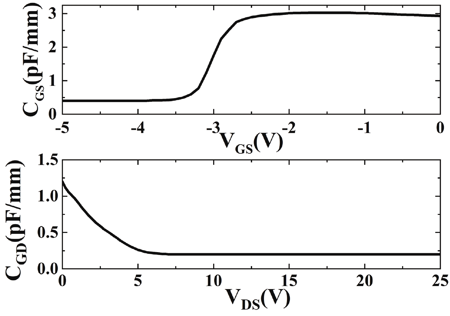
Fig. 1.
Relationship between capacitance and voltage for GaN HEMT.
REVIEWS
Chenglin Du1, 2, Ran Ye1, 2, , Xiaolong Cai1, 2, , Xiangyang Duan1, 2, Haijun Liu2, Yu Zhang2, Gang Qiu2 and Minhan Mi3
Corresponding author: Ran Ye, ye.ran@zte.com.cn; Xiaolong Cai, cai.xiaolong@zte.com.cn
Abstract: The GaN HEMT is a potential candidate for RF applications due to the high frequency and large power handling capability. To ensure the quality of the communication signal, linearity is a key parameter during the system design. However, the GaN HEMT usually suffers from the nonlinearity problems induced by the nonlinear parasitic capacitance, transconductance, channel transconductance etc. Among them, the transconductance reduction is the main contributor for the nonlinearity and is mostly attributed to the scattering effect, the increasing resistance of access region, the self-heating effect and the trapping effects. Based on the mechanisms, device-level improvement methods of transconductance including the trapping suppression, the nanowire channel, the graded channel, the double channel, the transconductance compensation and the new material structures have been proposed recently. The features of each method are reviewed and compared to provide an overview perspective on the linearity of the GaN HEMT at the device level.
Key words: GaN HEMT, linearity improvement, transconductance reduction, transconductance compensation, nanowire channel, graded channel
| [1] |
Jones E A, Wang F F, Costinett D. Review of commercial GaN power devices and GaN-based converter design challenges. IEEE J Emerg Sel Top Power Electron, 2016, 4, 707 doi: 10.1109/JESTPE.2016.2582685
|
| [2] |
Singh S, Chaudhary T, Khanna G. Recent advancements in wide band semiconductors (SiC and GaN) technology for future devices. Silicon, 2022, 14, 5793 doi: 10.1007/s12633-021-01362-3
|
| [3] |
Roccaforte F, Fiorenza P, Greco G, et al. Emerging trends in wide band gap semiconductors (SiC and GaN) technology for power devices. Microelectron Eng, 2018, 187/188, 66 doi: 10.1016/j.mee.2017.11.021
|
| [4] |
Aubry R, Jacquet J C, Oualli M, et al. ICP-CVD SiN passivation for high-power RF InAlGaN/GaN/SiC HEMT. IEEE Electron Device Lett, 2016, 37, 629 doi: 10.1109/LED.2016.2540164
|
| [5] |
Kumar V, Lu W, Schwindt R, et al. AlGaN/GaN HEMTs on SiC with fT of over 120 GHz. IEEE Electron Device Lett, 2002, 23, 455 doi: 10.1109/LED.2002.801303
|
| [6] |
Zhang Y C, Wei K, Huang S, et al. High-temperature-recessed millimeter-wave AlGaN/GaN HEMTs with 42.8% power-added-efficiency at 35 GHz. IEEE Electron Device Lett, 2018, 39, 727 doi: 10.1109/LED.2018.2822259
|
| [7] |
Du H H, Zhang J C, Zhou H, et al. GaN high-electron-mobility-transistor on free- standing GaN substrate with low contact resistance and state-of-the-art fT × LG value. IEEE Trans Electron Devices, 2022, 69, 968 doi: 10.1109/TED.2021.3138954
|
| [8] |
Micovic M, Brown D F, Regan D, et al. High frequency GaN HEMTs for RF MMIC applications. 2016 IEEE International Electron Devices Meeting (IEDM), 2016, 653 doi: 10.1109/IEDM.2016.7838337
|
| [9] |
Tan J, Yuk K S, Branner G R. Design of a high power, wideband power amplifier using AlGaN/GaN HEMT. 2017 IEEE 18th Wireless and Microwave Technology Conference (WAMICON), 2017, 1 doi: 10.1109/WAMICON.2017.7930252
|
| [10] |
Joshi R, Liu M H, Hsu S S H. A high efficiency compact class F GaN MMIC power amplifier for 5G applications. 2020 50th European Microwave Conference (EuMC), 2021, 1103 doi: 10.23919/EuMC48046.2021.9337963
|
| [11] |
Polli G, Del Gaudio A, De Padova A, et al. A high-performance C-band integrated front-end in AlGaN/GaN technology. 2018 International Workshop on Integrated Nonlinear Microwave and Millimetre-wave Circuits (INMMIC), Brive La Gaillarde, France, 2018, 1 doi: 10.1109/INMMIC.2018.8429986
|
| [12] |
Iucolano F, Boles T. GaN-on-Si HEMTs for wireless base stations. Mater Sci Semicond Process, 2019, 98, 100 doi: 10.1016/j.mssp.2019.03.032
|
| [13] |
Nunes L C, Cabral P M, Pedro J C. AM/AM and AM/PM distortion generation mechanisms in Si LDMOS and GaN HEMT based RF power amplifiers. IEEE Trans Microw Theory Tech, 2014, 62, 799 doi: 10.1109/TMTT.2014.2305806
|
| [14] |
Cheaito A, Crussiere M, Louet Y, et al. EVM derivation for multicarrier signals: Joint impact of non-linear amplification and predistortion. 2015 IEEE 81st Vehicular Technology Conference (VTC Spring), 2015, 1 doi: 10.1109/VTCSpring.2015.7145831
|
| [15] |
Pedro J C, Nunes L C, Cabral P M. Soft compression and the origins of nonlinear behavior of GaN HEMTs. 2014 9th European Microwave Integrated Circuit Conference, Rome, Italy, 2014, 1297 doi: 10.1109/EuMIC.2014.6997865
|
| [16] |
Kobayashi K W. Bias optimized IP2 & IP3 linearity and NF of a decade-bandwidth GaN MMIC feedback amplifier. 2012 IEEE Radio Frequency Integrated Circuits Symposium, Montreal, QC, Canada, 2012, 479 doi: 10.1109/RFIC.2012.6242326
|
| [17] |
Guan L, Zhu A D. Green communications: Digital predistortion for wideband RF power amplifiers. IEEE Microw Mag, 2014, 15(7), 84 doi: 10.1109/MMM.2014.2356037
|
| [18] |
Choi P, Radhakrishna U, Boon C C, et al. Linearity enhancement of a fully integrated 6-GHz GaN power amplifier. IEEE Microw Wirel Compon Lett, 2017, 27, 927 doi: 10.1109/LMWC.2017.2746673
|
| [19] |
Ren J J. A new digital predistortion algorithms scheme of feedback FIR cross-term memory polynomial model for short-wave power amplifier. IEEE Access, 2020, 8, 38327 doi: 10.1109/ACCESS.2020.2976152
|
| [20] |
Tomé P M, Barradas F M, Cunha T R, et al. Hybrid analog/digital linearization of GaN HEMT-based power amplifiers. IEEE Trans Microw Theory Tech, 2019, 67, 288 doi: 10.1109/TMTT.2018.2880911
|
| [21] |
Abuelma'atti M T, Abuelmaatti A M T, Yeung T, et al. Linearization of GaN power amplifier using feedforward and predistortion techniques. 2011 3rd Asia Symposium on Quality Electronic Design (ASQED), Kuala Lumpur, Malaysia, 2011, 282 doi: 10.1109/ASQED.2011.6111761
|
| [22] |
Moore K, Green B, Klingbeil S, et al. High performance 150 mm RF GaN technology with low memory effects. 2020 IEEE BiCMOS and Compound Semiconductor Integrated Circuits and Technology Symposium (BCICTS), Monterey, CA, USA, 2021, 1 doi: 10.1109/BCICTS48439.2020.9392951
|
| [23] |
Lin C K, Du J H, Wang A, et al. Pure-play GaN foundry technology for RF applications. 2014 Asia-Pacific Microwave Conference, Sendai, Japan, 2015, 188
|
| [24] |
Nayak S, Kao M Y, Chen H T, et al. 0.15 μm GaN MMIC manufacturing technology for 2-50 GHz power applications. Conference on Compound Semiconductor Manufacturing Technology, Scottsdale, Arizona, USA, 2015, 43
|
| [25] |
Nagy W, Brown J, Borges R, et al. Linearity characteristics of microwave-power GaN HEMTs. IEEE Trans Microw Theory Tech, 2003, 51, 660 doi: 10.1109/TMTT.2002.807684
|
| [26] |
Srinidhi E R, Kompa G. Investigation of IMD3 in GaN HEMT based on extended volterra series analysis. 2007 European Microwave Integrated Circuit Conference, Munich, Germany, 2007, 52 doi: 10.1109/EMICC.2007.4412645
|
| [27] |
Ahmed A, Islam S S, Anwar A F M. A temperature-dependent nonlinear analysis of GaN/AlGaN HEMTs using Volterra series. IEEE Trans Microw Theory Tech, 2001, 49, 1518 doi: 10.1109/22.942561
|
| [28] |
Garcia J A, Sanchez A M, Pedro J C, et al. Characterizing the gate-to-source nonlinear capacitor role on GaAs FET IMD performance. IEEE Trans Microw Theory Tech, 1998, 46, 2344 doi: 10.1109/22.739222
|
| [29] |
Sarbishaei H, Wu D Y T, Boumaiza S. Linearity of GaN HEMT RF power amplifiers-a circuit perspective. 2012 IEEE/MTT-S International Microwave Symposium Digest, Montreal, QC, Canada, 2012, 1 doi: 10.1109/MWSYM.2012.6259553
|
| [30] |
Joglekar S, Radhakrishna U, Piedra D, et al. Large signal linearity enhancement of AlGaN/GaN high electron mobility transistors by device-level Vt engineering for transconductance compensation. 2017 IEEE International Electron Devices Meeting (IEDM), San Francisco, CA, USA, 2018, 25.3.1 doi: 10.1109/IEDM.2017.8268457
|
| [31] |
Maas S A. Nonlinear microwave and RF circuits. 2nd ed. Artech House, 1997
|
| [32] |
Tarakji A, Fatima H, Hu X, et al. Large-signal linearity in III-N MOSDHFETs. IEEE Electron Device Lett, 2003, 24, 369 doi: 10.1109/LED.2003.813355
|
| [33] |
Garcia J A, Aballo T, Mediavilla A, et al. Characterizing the Igs(Vgs) nonlinearity for describing its contribution to FET large-signal intermodulation distortion. 2006 International Workshop on Integrated Nonlinear Microwave and Millimeter-Wave Circuits, Aveiro, Portugal, 2006, 80 doi: 10.1109/INMMIC.2006.283514
|
| [34] |
Liu Z H, Ng G I, Arulkumaran S, et al. Improved linearity for low-noise applications in 0.25-μm GaN MISHEMTs using ALD Al2O3 as gate dielectric. IEEE Electron Device Lett, 2010, 31, 803 doi: 10.1109/LED.2010.2051136
|
| [35] |
Oxley C H, Uren M J, Coates A, et al. On the temperature and carrier density dependence of electron saturation velocity in an AlGaN/GaN HEMT. IEEE Trans Electron Devices, 2006, 53, 565 doi: 10.1109/TED.2005.863540
|
| [36] |
Ridley B K, Schaff W J, Eastman L F. Hot-phonon-induced velocity saturation in GaN. J Appl Phys, 2004, 96, 1499 doi: 10.1063/1.1762999
|
| [37] |
Fang T, Wang R H, Xing H L, et al. Effect of optical phonon scattering on the performance of GaN transistors. IEEE Electron Device Lett, 2012, 33, 709 doi: 10.1109/LED.2012.2187169
|
| [38] |
Bajaj S, Shoron O F, Park P S, et al. Density-dependent electron transport and precise modeling of GaN high electron mobility transistors. Appl Phys Lett, 2015, 107, 153504 doi: 10.1063/1.4933181
|
| [39] |
Juang J R, Huang T Y, Chen T M, et al. Transport in a gated Al0.18Ga0.82N/GaN electron system. J Appl Phys, 2003, 94, 3181 doi: 10.1063/1.1594818
|
| [40] |
Li T, Joshi R P, Fazi C. Monte Carlo evaluations of degeneracy and interface roughness effects on electron transport in AlGaN–GaN heterostructures. J Appl Phys, 2000, 88, 829 doi: 10.1063/1.373744
|
| [41] |
Palacios T, Rajan S, Chakraborty A, et al. Influence of the dynamic access resistance in the g/sub m/and f/sub T/linearity of AlGaN/GaN HEMTs. IEEE Trans Electron Devices, 2005, 52, 2117 doi: 10.1109/TED.2005.856180
|
| [42] |
Tirado J M, Mieville F, Zhao X, et al. Origin of the increasing access resistance in AlGaN/GaN HEMTs. 2008 Device Research Conference, Santa Barbara, CA, USA, 2008, 203 doi: 10.1109/DRC.2008.4800803
|
| [43] |
Wu Y R, Singh M, Singh J. Sources of transconductance collapse in III-V nitrides-consequences of velocity-field relations and source/gate design. IEEE Trans Electron Devices, 2005, 52, 1048 doi: 10.1109/TED.2005.848084
|
| [44] |
Trew R J, Liu Y Y, Bilbro L, et al. Nonlinear source resistance in high-voltage microwave AlGaN/GaN HFETs. IEEE Trans Microw Theory Tech, 2006, 54, 2061 doi: 10.1109/TMTT.2006.873627
|
| [45] |
Yang M, Lin Z J, Zhao J T, et al. Effect of polarization coulomb field scattering on parasitic source access resistance and extrinsic transconductance in AlGaN/GaN heterostructure FETs. IEEE Trans Electron Devices, 2016, 63, 1471 doi: 10.1109/TED.2016.2532919
|
| [46] |
Chen C H, Sadler R, Wang D, et al. The causes of GaN HEMT bell-shaped transconductance degradation. Solid State Electron, 2016, 126, 115 doi: 10.1016/j.sse.2016.09.005
|
| [47] |
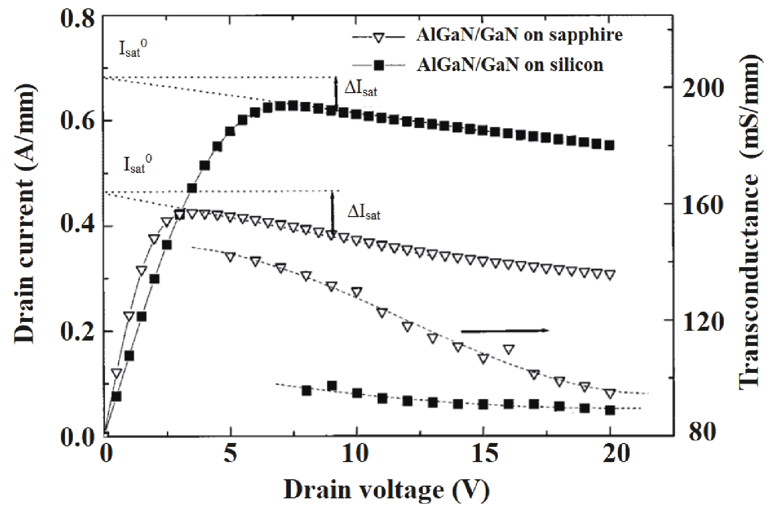
Kuzmik J, Javorka R, Alam A, et al. Determination of channel temperature in AlGaN/GaN HEMTs grown on sapphire and silicon substrates using DC characterization method. IEEE Trans Electron Devices, 2002, 49, 1496 doi: 10.1109/TED.2002.801430
|
| [48] |
Mitrofanov O, Manfra M. Mechanisms of gate lag in GaN/AlGaN/GaN high electron mobility transistors. Superlattices Microstruct, 2003, 34, 33 doi: 10.1016/j.spmi.2003.12.002
|
| [49] |
Tirado J M, Sanchez-Rojas J L, Izpura J I. Trapping effects in the transient response of AlGaN/GaN HEMT devices. IEEE Trans Electron Devices, 2007, 54, 410 doi: 10.1109/TED.2006.890592
|
| [50] |
Hu W D, Chen X S, Lu W. Intrinsic mechanism of drain-lag and current collapse in GaN-based HEMTs. 2009 IEEE Workshop on Microelectronics and Electron Devices, Boise, ID, USA, 2009, 1 doi: 10.1109/WMED.2009.4816142
|
| [51] |
Binari S C, Ikossi K, Roussos J A, et al. Trapping effects and microwave power performance in AlGaN/GaN HEMTs. IEEE Trans Electron Devices, 2001, 48, 465 doi: 10.1109/16.906437
|
| [52] |
Meneghesso G, Verzellesi G, Pierobon R, et al. Surface-related drain current dispersion effects in AlGaN-GaN HEMTs. IEEE Trans Electron Devices, 2004, 51, 1554 doi: 10.1109/TED.2004.835025
|
| [53] |
Mollah S, Gaevski M, Hussain K, et al. Current collapse in high-Al channel AlGaN HFETs. Appl Phys Express, 2019, 12, 074001 doi: 10.7567/1882-0786/ab24b1
|
| [54] |
Tirado J M, Sanchez-Rojas J L, Izpura J I. Simulation of surface state effects in the transient response of AlGaN/GaN HEMT and GaN MESFET devices. Semicond Sci Technol, 2006, 21, 1150 doi: 10.1088/0268-1242/21/8/029
|
| [55] |
Meneghini M, Ronchi N, Stocco A, et al. Investigation of trapping and hot-electron effects in GaN HEMTs by means of a combined electrooptical method. IEEE Trans Electron Devices, 2011, 58, 2996 doi: 10.1109/TED.2011.2160547
|
| [56] |
Vetury R, Zhang N Q, Keller S, et al. The impact of surface states on the DC and RF characteristics of AlGaN/GaN HFETs. IEEE Trans Electron Devices, 2001, 48, 560 doi: 10.1109/16.906451
|
| [57] |
Saito Y, Tsurumaki R, Noda N, et al. Analysis of reduction in lag phenomena and current collapse in field-plate AlGaN/GaN HEMTs with high acceptor density in a buffer layer. IEEE Trans Device Mater Reliab, 2018, 18(1), 46 doi: 10.1109/TDMR.2017.2779429
|
| [58] |
Meneghesso G, Meneghini M, Bisi D, et al. Trapping phenomena in AlGaN/GaN HEMTs: A study based on pulsed and transient measurements. Semicond Sci Technol, 2013, 28, 074021 doi: 10.1088/0268-1242/28/7/074021
|
| [59] |
Du J F, Chen N T, Jiang Z G, et al. Study on transconductance non-linearity of AlGaN/GaN HEMTs considering acceptor-like traps in barrier layer under the gate. Solid State Electron, 2016, 115, 60 doi: 10.1016/j.sse.2015.10.008
|
| [60] |
Binari S C, Klein P B, Kazior T E. Trapping effects in GaN and SiC microwave FETs. Proc IEEE, 2002, 90, 1048 doi: 10.1109/JPROC.2002.1021569
|
| [61] |
Kohn E, Daumiller I, Schmid P, et al. Large signal frequency dispersion of AlGaN/GaN heterostructure field effect transistors. Electron Lett, 1999, 35, 1022 doi: 10.1049/el:19990697
|
| [62] |
Xie S X, Paidi V, Heikman S, et al. High linearity GaN HEMT power amplifier with pre-linearization gate diode. IEEE Lester Eastman Conference on High Performance Devices, Troy, NY, USA, 2004, 223 doi: 10.1109/LECHPD.2004.1549698
|
| [63] |
Bothe K M, Ganguly S, Guo J, et al. Improved X-band performance and reliability of a GaN HEMT with Sunken source connected field plate design. IEEE Electron Device Lett, 2022, 43, 354 doi: 10.1109/LED.2022.3146194
|
| [64] |
Wu Y F, Saxler A, Moore M, et al. 30-W/mm GaN HEMTs by field plate optimization. IEEE Electron Device Lett, 2004, 25, 117 doi: 10.1109/LED.2003.822667
|
| [65] |
Brown D F, Tang Y, Regan D A, et al. Self-aligned AlGaN/GaN FinFETs. IEEE Electron Device Lett, 2017, 38, 1445 doi: 10.1109/LED.2017.2747843
|
| [66] |
Zhang J Q, Wang L, Li L A, et al. Self-aligned-gate AlGaN/GaN heterostructure field-effect transistor with titanium nitride gate. Chin Phys B, 2016, 25, 087308 doi: 10.1088/1674-1056/25/8/087308
|
| [67] |
Khalil I, Bahat-Treidel E, Schnieder F, et al. Improving the linearity of GaN HEMTs by optimizing epitaxial structure. IEEE Trans Electron Devices, 2009, 56, 361 doi: 10.1109/TED.2008.2011849
|
| [68] |
Aggarwal R, Agrawal A, Gupta M, et al. Improved linearity performance of AlGaN/GaN MISHFET over conventional HFETs: An optimization study for wireless infrastructure applications. Superlattices Microstruct, 2011, 50, 1 doi: 10.1016/j.spmi.2011.03.009
|
| [69] |
Hasan M T, Asano T, Tokuda H, et al. Current collapse suppression by gate field-plate in AlGaN/GaN HEMTs. IEEE Electron Device Lett, 2013, 34, 1379 doi: 10.1109/LED.2013.2280712
|
| [70] |
Suemitsu T, Kobayashi K, Hatakeyama S, et al. A new process approach for slant field plates in GaN-based high-electron-mobility transistors. Jpn J Appl Phys, 2016, 55, 01AD02 doi: 10.7567/JJAP.55.01AD02
|
| [71] |
Shao J H, Deng J N, Lu W, et al. Nanofabrication of 80 nm asymmetric T shape gates for GaN HEMTs. Microelectron Eng, 2018, 189, 6 doi: 10.1016/j.mee.2017.12.001
|
| [72] |
Arulkumaran S, Egawa T, Ishikawa H, et al. Surface passivation effects on AlGaN/GaN high-electron-mobility transistors with SiO2, Si3N4, and silicon oxynitride. Appl Phys Lett, 2004, 84, 613 doi: 10.1063/1.1642276
|
| [73] |
Vertiatchikh A V, Eastman L F, Schaff W J, et al. Effect of surface passivation of AlGaN/GaN heterostructure field-effect transistor. Electron Lett, 2002, 38, 388 doi: 10.1049/el:20020270
|
| [74] |
Bernát J, Javorka P, Fox A, et al. Effect of surface passivation on performance of AlGaN/GaN/Si HEMTs. Solid State Electron, 2003, 47, 2097 doi: 10.1016/S0038-1101(03)00238-7
|
| [75] |
Luo B, Johnson J W, Kim J, et al. Influence of MgO and Sc2O3 passivation on AlGaN/GaN high-electron-mobility transistors. Appl Phys Lett, 2002, 80, 1661 doi: 10.1063/1.1455692
|
| [76] |
Gila B P, Thaler G T, Onstine A H, et al. New dielectrics for gate oxides and surface passivation on GaN. 2005 International Semiconductor Device Research Symposium, Bethesda, MD, USA, 2005, 130 doi: 10.1109/ISDRS.2005.1596014
|
| [77] |
Joglekar S, Azize M, Jones E J, et al. Impact of Al2O3 passivation on AlGaN/GaN nanoribbon high-electron-mobility transistors. IEEE Trans Electron Devices, 2016, 63, 318 doi: 10.1109/TED.2015.2500159
|
| [78] |
Koehler A D, Nepal N, Anderson T J, et al. Atomic layer epitaxy AlN for enhanced AlGaN/GaN HEMT passivation. IEEE Electron Device Lett, 2013, 34, 1115 doi: 10.1109/LED.2013.2274429
|
| [79] |
Oh M, Yang J W, Kim H, et al. Electrical characteristics of AlGaN/GaN high-electron-mobility transistors fabricated with a MgF2 passivation layer. J Korean Phys Soc, 2020, 76, 278 doi: 10.3938/jkps.76.278
|
| [80] |
Lin Y S, Lin S F, Hsu W C. Microwave and power characteristics of AlGaN/GaN/Si high-electron mobility transistors with HfO2 and TiO2 passivation. Semicond Sci Technol, 2015, 30, 015016 doi: 10.1088/0268-1242/30/1/015016
|
| [81] |
Green B M, Chu K K, Chumbes E M, et al. The effect of surface passivation on the microwave characteristics of undoped AlGaN/GaN HEMTs. IEEE Electron Device Lett, 2000, 21, 268 doi: 10.1109/55.843146
|
| [82] |
Ansell B J, Harrison I, Foxon C T. The effect of surface passivation and illumination on the device properties of AlGaN/GaN HFETs. Phys Stat Sol (a), 2001, 188, 279 doi: 10.1002/1521-396X(200111)188:1<279::AID-PSSA279>3.0.CO;2-Y
|
| [83] |
Lu W, Kumar V, Schwindt R, et al. A comparative study of surface passivation on AlGaN/GaN HEMTs. Solid State Electron, 2002, 46, 1441 doi: 10.1016/S0038-1101(02)00089-8
|
| [84] |
Liu J L, Mi M H, Zhu J J, et al. Improved power performance and the mechanism of AlGaN/GaN HEMTs using Si-rich SiN/Si3N4 bilayer passivation. IEEE Trans Electron Devices, 2022, 69, 631 doi: 10.1109/TED.2021.3133822
|
| [85] |
Jing G J, Wang X H, Huang S, et al. Mechanism of linearity improvement in GaN HEMTs by low pressure chemical vapor deposition-SiNx passivation. IEEE Trans Electron Devices, 2022, 69, 6610 doi: 10.1109/TED.2022.3213636
|
| [86] |
Kordoš P, Bernát J, Marso M. Impact of layer structure on performance of unpassivated AlGaN/GaN HEMT. Microelectron J, 2005, 36, 438 doi: 10.1016/j.mejo.2005.02.040
|
| [87] |
Meneghesso G, Rampazzo F, Kordos P, et al. Current collapse and high-electric-field reliability of unpassivated GaN/AlGaN/GaN HEMTs. IEEE Trans Electron Devices, 2006, 53, 2932 doi: 10.1109/TED.2006.885681
|
| [88] |
Kikkawa T, Nagahara M, Okamoto N, et al. Surface-charge controlled AlGaN/GaN-power HFET without current collapse and gm dispersion. International Electron Devices Meeting. Technical Digest (Cat. No.01CH37224), Washington, DC, USA, 2001, 25.4.1 doi: 10.1109/IEDM.2001.979574
|
| [89] |
Mitrofanov O, Manfra M, Weimann N. Impact of Si doping on radio frequency dispersion in unpassivated GaN/AlGaN/GaN high-electron-mobility transistors grown by plasma-assisted molecular-beam epitaxy. Appl Phys Lett, 2003, 82, 4361 doi: 10.1063/1.1582373
|
| [90] |
Uren M J, Moreke J, Kuball M. Buffer design to minimize current collapse in GaN/AlGaN HFETs. IEEE Trans Electron Devices, 2012, 59, 3327 doi: 10.1109/TED.2012.2216535
|
| [91] |
Chen D Y, Malmros A, Thorsell M, et al. Microwave performance of ‘buffer-free’ GaN-on-SiC high electron mobility transistors. IEEE Electron Device Lett, 2020, 41, 828 doi: 10.1109/LED.2020.2988074
|
| [92] |
Yao Y X, Huang S, Jiang Q M, et al. Identification of semi-ON-state current collapse in AlGaN/GaN HEMTs by drain current deep level transient spectroscopy. IEEE Electron Device Lett, 2022, 43, 200 doi: 10.1109/LED.2021.3135900
|
| [93] |
Kumazaki Y, Ohki T, Kotani J, et al. Over 80% power-added-efficiency GaN high-electron-mobility transistors on free-standing GaN substrates. Appl Phys Express, 2021, 14, 016502 doi: 10.35848/1882-0786/abc1cc
|
| [94] |
Ye R, Cai X L, Du C L, et al. An overview on analyses and suppression methods of trapping effects in AlGaN/GaN HEMTs. IEEE Access, 2022, 10, 21759 doi: 10.1109/ACCESS.2021.3139443
|
| [95] |
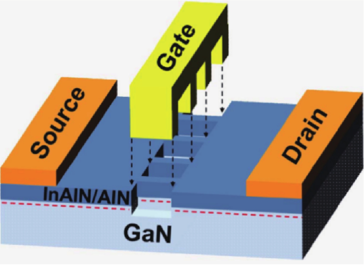
Lee D S, Wang H, Hsu A, et al. Nanowire channel InAlN/GaN HEMTs with high linearity of gm and fT. IEEE Electron Device Lett, 2013, 34, 969 doi: 10.1109/LED.2013.2261913
|
| [96] |
Hisamoto D, Lee W C, Kedzierski J, et al. FinFET-a self-aligned double-gate MOSFET scalable to 20 nm. IEEE Trans Electron Devices, 2000, 47, 2320 doi: 10.1109/16.887014
|
| [97] |
Zhang Y H, Zubair A, Liu Z H, et al. GaN FinFETs and trigate devices for power and RF applications: Review and perspective. Semicond Sci Technol, 2021, 36, 054001 doi: 10.1088/1361-6641/abde17
|
| [98] |
Lu B, Matioli E, Palacios T. Tri-gate normally-off GaN power MISFET. IEEE Electron Device Lett, 2012, 33, 360 doi: 10.1109/LED.2011.2179971
|
| [99] |
Zhang M, Ma X H, Yang L, et al. Influence of fin configuration on the characteristics of AlGaN/GaN fin-HEMTs. IEEE Trans Electron Devices, 2018, 65, 1745 doi: 10.1109/TED.2018.2819178
|
| [100] |
Zhang K, Kong Y C, Zhu G R, et al. High-linearity AlGaN/GaN FinFETs for microwave power applications. IEEE Electron Device Lett, 2017, 38, 615 doi: 10.1109/LED.2017.2687440
|
| [101] |
Shinohara K, King C, Carter A D, et al. GaN-based field-effect transistors with laterally gated two-dimensional electron gas. IEEE Electron Device Lett, 2018, 39, 417 doi: 10.1109/LED.2018.2797940
|
| [102] |
Odabaşı O, Yılmaz D, Aras E, et al. AlGaN/GaN-based laterally gated high-electron-mobility transistors with optimized linearity. IEEE Trans Electron Devices, 2021, 68, 1016 doi: 10.1109/TED.2021.3053221
|
| [103] |
Chang J, Afroz S, Nagamatsu K, et al. The super-lattice castellated field-effect transistor: A high-power, high-performance RF amplifier. IEEE Electron Device Lett, 2019, 40, 1048 doi: 10.1109/LED.2019.2917285
|
| [104] |
Shinohara K, King C, Regan E J, et al. GaN-based multi-channel transistors with lateral gate for linear and efficient millimeter-wave power amplifiers. 2019 IEEE MTT-S International Microwave Symposium (IMS), Boston, MA, USA, 2019, 1133 doi: 10.1109/MWSYM.2019.8700845
|
| [105] |
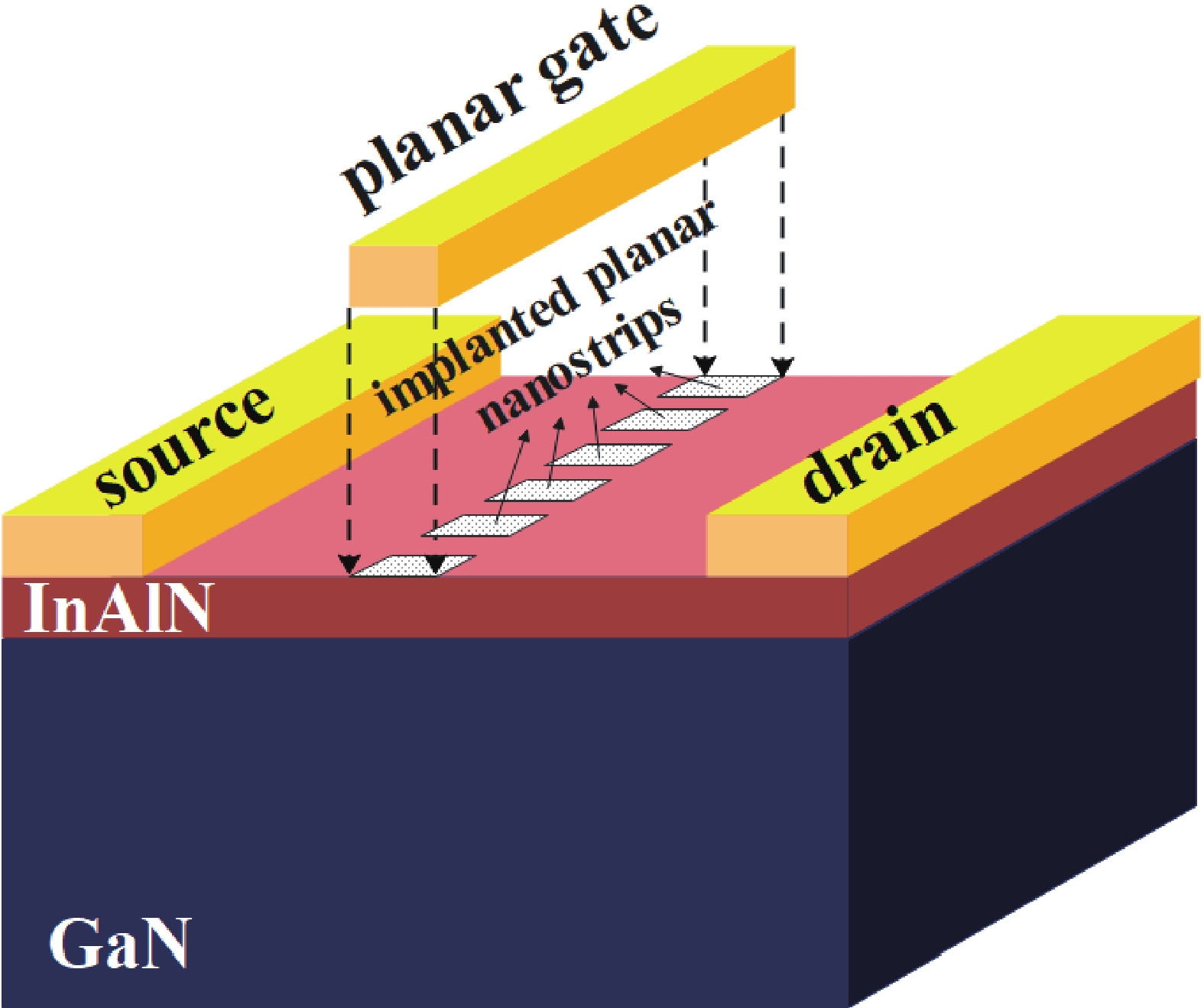
Xing W C, Liu Z H, Qiu H D, et al. Planar-nanostrip-channel InAlN/GaN HEMTs on Si with improved gm and fT linearity. IEEE Electron Device Lett, 2017, 38, 619 doi: 10.1109/LED.2017.2689810
|
| [106] |
Jena D, Heikman S, Green D, et al. Realization of wide electron slabs by polarization bulk doping in graded III–V nitride semiconductor alloys. Appl Phys Lett, 2002, 81, 4395 doi: 10.1063/1.1526161
|
| [107] |
Fang Y L, Feng Z H, Yin J Y, et al. AlGaN/GaN polarization-doped field-effect transistors with graded heterostructure. IEEE Trans Electron Devices, 2014, 61, 4084 doi: 10.1109/TED.2014.2364457
|
| [108] |
Bajaj S, Yang Z C, Akyol F, et al. Graded AlGaN channel transistors for improved current and power gain linearity. IEEE Trans Electron Devices, 2017, 64, 3114 doi: 10.1109/TED.2017.2713784
|
| [109] |
Sohel S H, Xie A, Beam E, et al. X-band power and linearity performance of compositionally graded AlGaN channel transistors. IEEE Electron Device Lett, 2018, 39, 1884 doi: 10.1109/LED.2018.2874443
|
| [110] |
Fang Y L, Song X B, Feng Z H, et al. High linearity step-graded AlGaN/GaN heterojunction field effect transistor. 2016 13th China International Forum on Solid State Lighting: International Forum on Wide Bandgap Semiconductors China (SSLChina: IFWS), Beijing, China, 2016, 104 doi: 10.1109/IFWS.2016.7803768
|
| [111] |
Sohel S H, Xie A, Beam E, et al. Polarization engineering of AlGaN/GaN HEMT with graded InGaN sub-channel for high-linearity X-band applications. IEEE Electron Device Lett, 2019, 40, 522 doi: 10.1109/LED.2019.2899100
|
| [112] |
Moon J S, Wong J, Grabar B, et al. 360 GHz fMAX graded-channel AlGaN/GaN HEMTs for mmW low-noise applications. IEEE Electron Device Lett, 2020, 41, 1173 doi: 10.1109/LED.2020.3005337
|
| [113] |
Moon J S, Grabar B, Antcliffe M, et al. High-speed graded-channel GaN HEMTs with linearity and efficiency. 2020 IEEE/MTT-S International Microwave Symposium (IMS), Los Angeles, CA, USA, 2020, 573 doi: 10.1109/IMS30576.2020.9223775
|
| [114] |
Hou B, Yang L, Mi M H, et al. High linearity and high power performance with barrier layer of sandwich structure and Al0.05GaN back barrier for X-band application. J Phys D: Appl Phys, 2020, 53, 145102 doi: 10.1088/1361-6463/ab678f
|
| [115] |
Liu J, Zhou Y G, Chu R M, et al. Al0.3Ga0.7N/Al0.05Ga0.95N/GaN composite-channel HEMTs with enhanced linearity. IEDM Technical Digest. IEEE International Electron Devices Meeting, San Francisco, CA, USA, 2004, 811 doi: 10.1109/IEDM.2004.1419299
|
| [116] |
Liu J E, Zhou Y G, Chu R M, et al. Highly linear Al0.3Ga0.7N-Al0.05Ga0.95N-GaN composite-channel HEMTs. IEEE Electron Device Lett, 2005, 26, 145 doi: 10.1109/LED.2005.843218
|
| [117] |
Song W J, Zheng Z Y, Chen T, et al. RF linearity enhancement of GaN-on-Si HEMTs with a closely coupled double-channel structure. IEEE Electron Device Lett, 2021, 42, 1116 doi: 10.1109/LED.2021.3087785
|
| [118] |
Yu Q, Shi C Z, Yang L, et al. High current and linearity AlGaN/GaN/-graded-AlGaN: Si-doped/GaN heterostructure for low voltage power amplifier application. IEEE Electron Device Lett, 2023, 44, 582 doi: 10.1109/LED.2023.3241763
|
| [119] |
Palacios T, Chini A, Buttari D, et al. Use of double-channel heterostructures to improve the access resistance and linearity in GaN-based HEMTs. IEEE Trans Electron Devices, 2006, 53, 562 doi: 10.1109/TED.2005.863767
|
| [120] |
Choi W, Chen R J, Levy C, et al. Intrinsically linear transistor for millimeter-wave low noise amplifiers. Nano Lett, 2020, 20, 2812 doi: 10.1021/acs.nanolett.0c00522
|
| [121] |
Wang P F, Ma X H, Mi M H, et al. Influence of fin-like configuration parameters on the linearity of AlGaN/GaN HEMTs. IEEE Trans Electron Devices, 2021, 68, 1563 doi: 10.1109/TED.2021.3062561
|
| [122] |
Wu S, Ma X H, Yang L, et al. A millimeter-wave AlGaN/GaN HEMT fabricated with transitional-recessed-gate technology for high-gain and high-linearity applications. IEEE Electron Device Lett, 2019, 40, 846 doi: 10.1109/LED.2019.2909770
|
| [123] |
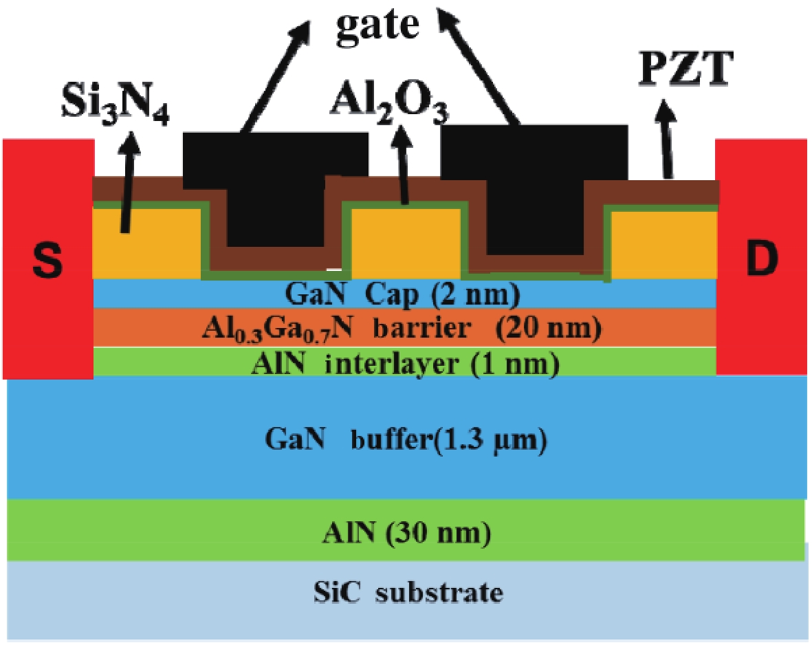
Gao T, Xu R M, Kong Y C, et al. Improved linearity in AlGaN/GaN metal-insulator-semiconductor high electron mobility transistors with nonlinear polarization dielectric. Appl Phys Lett, 2015, 106, 243501 doi: 10.1063/1.4922724
|
| [124] |
Zhang Y C, Zhang T, Zhou H, et al. InGaN-channel high-electron-mobility transistor with enhanced linearity and high-temperature performance. Appl Phys Express, 2018, 11, 094101 doi: 10.7567/APEX.11.094101
|
| [125] |
Wong M H, Keller S, Dasgupta N S, et al. N-polar GaN epitaxy and high electron mobility transistors. Semicond Sci Technol, 2013, 28, 074009 doi: 10.1088/0268-1242/28/7/074009
|
| [126] |
Arias A, Rowell P, Bergman J, et al. High performance N-polar GaN HEMTs with OIP3/Pdc ~12dB at 10GHz. 2017 IEEE Compound Semiconductor Integrated Circuit Symposium (CSICS), Miami, FL, USA, 2017, 1 doi: 10.1109/CSICS.2017.8240456
|
| [127] |
Guidry M, Romanczyk B, Li H, et al. Demonstration of 30 GHz OIP3/PDC > 10 dB by mm-wave N-polar deep recess MISHEMTs. 2019 14th European Microwave Integrated Circuits Conference (EuMIC), Paris, France, 2019, 64 doi: 10.23919/EuMIC.2019.8909579
|
| [128] |
Shrestha P, Guidry M, Romanczyk B, et al. High linearity and high gain performance of N-polar GaN MIS-HEMT at 30 GHz. IEEE Electron Device Lett, 2020, 41, 681 doi: 10.1109/LED.2020.2980841
|
| [129] |
Wang H C, Su H F, Luc Q H, et al. Improved linearity in AlGaN/GaN HEMTs for millimeter-wave applications by using dual-gate fabrication. ECS J Solid State Sci Technol, 2017, 6, S3106 doi: 10.1149/2.0251711jss
|
| [130] |
Panda D K, Lenka T R. Linearity improvement in E-mode ferroelectric GaN MOS-HEMT using dual gate technology. Micro Nano Lett, 2019, 14, 618 doi: 10.1049/mnl.2018.5499
|
| [131] |
Fichtenbaum N A, Schaake C, Mates T E, et al. Electrical characterization of p-type N-polar and Ga-polar GaN grown by metalorganic chemical vapor deposition. Appl Phys Lett, 2007, 91, 172105 doi: 10.1063/1.2800304
|
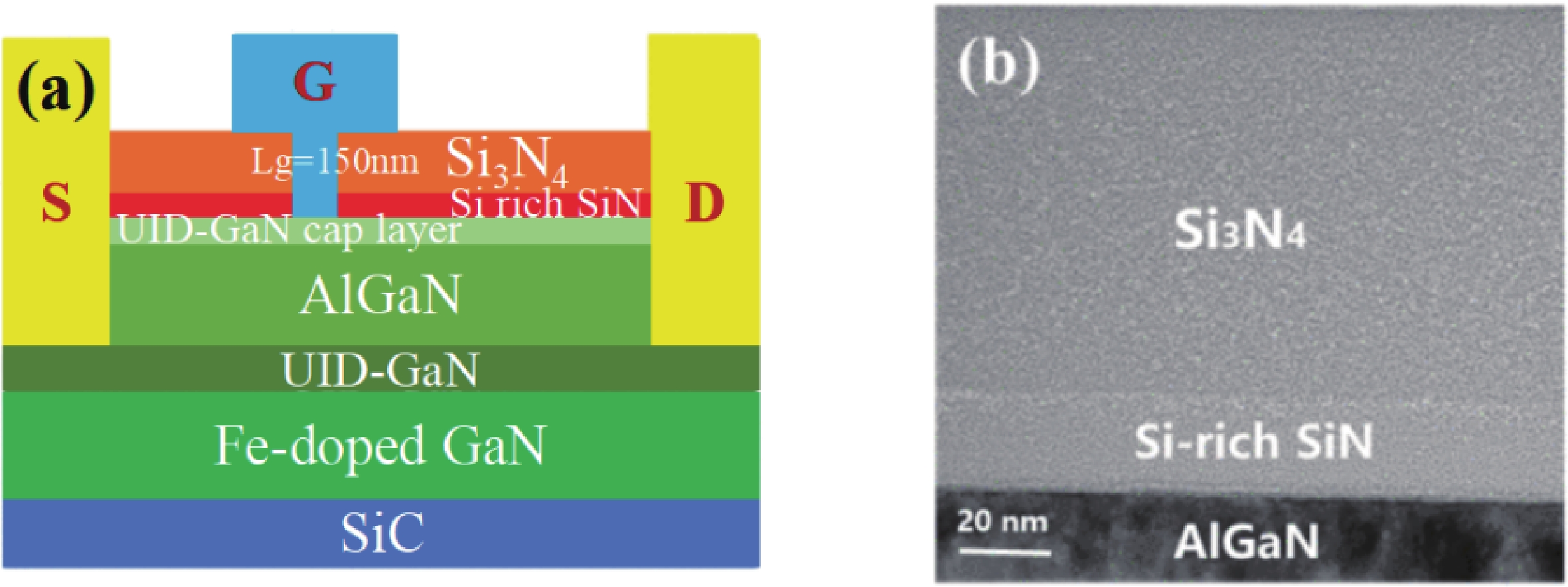
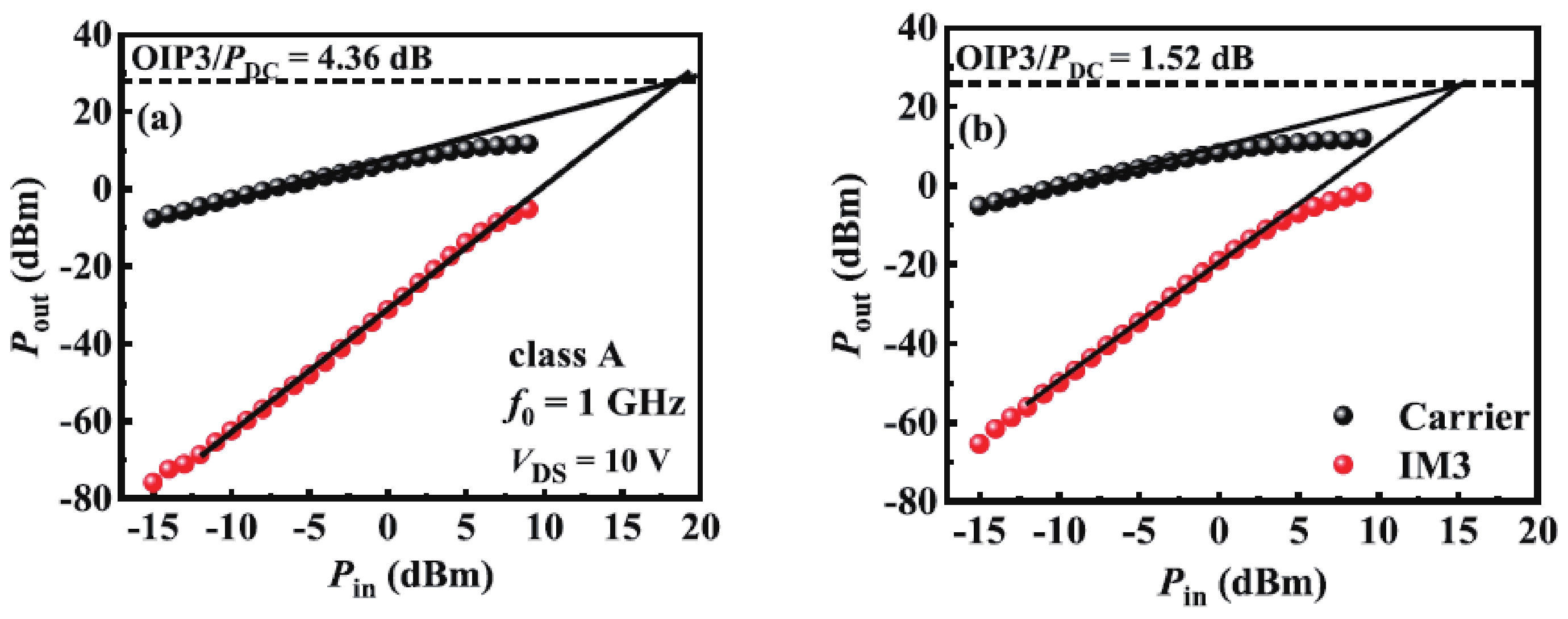
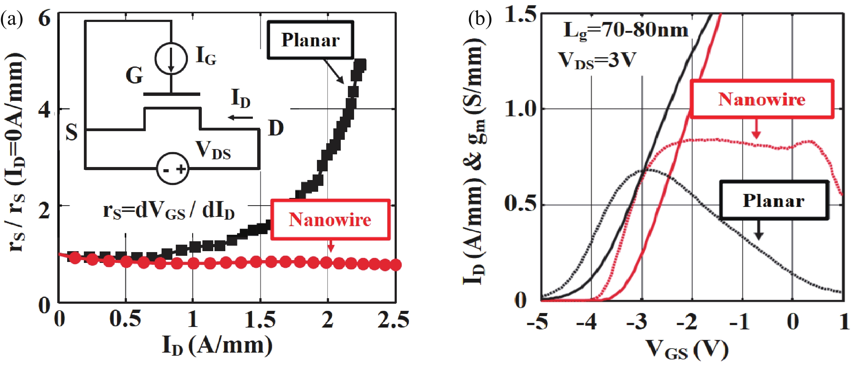
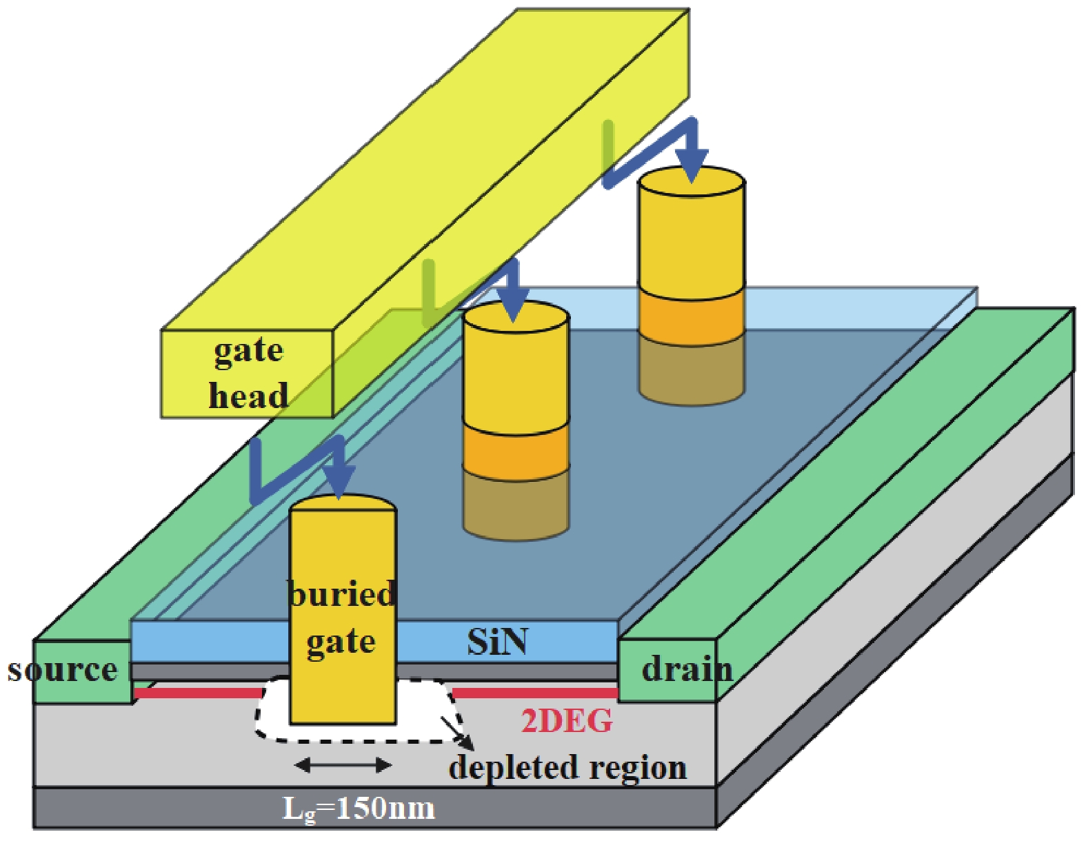
Table 1. Features of reported improvement methods for nonlinear gm.
| Types | Mechanisms | Challenges |
| Trapping suppression | Reduce the electric field; eliminate the sources of the traps; keep the 2DEG from the traps |
Mostly have no ability to further improve the GVS |
| Nanowire channel (fin structure/tri-gate) | Effectively suppress the increasing of rS due to the large current drivability | Extra parasitic gate capacitance; loss of the output current; etching damage risk |
| Graded channel (PolFET with 3DEG) | Maintain the stable electron volume to suppress scattering | Low peak gm; complex epitaxy process of the graded channel |
| Double channel | Reduce perpendicular electric field; electron compensation between double channel |
Multiple epitaxy of the double channel |
| gm compensation | Different gm compensated with each other | Precise design for threshold voltage; hard process control for stable threshold |
| Ferroelectric dielectric/N-polar hetero-structure | Nonlinear polarization effect of PZT / improvement of electron confinement | Tough epitaxy growth of N-polar |
| Double gate | Alleviate the electric field | Low peak gm |
 DownLoad: CSV
| [1] |
Jones E A, Wang F F, Costinett D. Review of commercial GaN power devices and GaN-based converter design challenges. IEEE J Emerg Sel Top Power Electron, 2016, 4, 707 doi: 10.1109/JESTPE.2016.2582685
|
| [2] |
Singh S, Chaudhary T, Khanna G. Recent advancements in wide band semiconductors (SiC and GaN) technology for future devices. Silicon, 2022, 14, 5793 doi: 10.1007/s12633-021-01362-3
|
| [3] |
Roccaforte F, Fiorenza P, Greco G, et al. Emerging trends in wide band gap semiconductors (SiC and GaN) technology for power devices. Microelectron Eng, 2018, 187/188, 66 doi: 10.1016/j.mee.2017.11.021
|
| [4] |
Aubry R, Jacquet J C, Oualli M, et al. ICP-CVD SiN passivation for high-power RF InAlGaN/GaN/SiC HEMT. IEEE Electron Device Lett, 2016, 37, 629 doi: 10.1109/LED.2016.2540164
|
| [5] |
Kumar V, Lu W, Schwindt R, et al. AlGaN/GaN HEMTs on SiC with fT of over 120 GHz. IEEE Electron Device Lett, 2002, 23, 455 doi: 10.1109/LED.2002.801303
|
| [6] |
Zhang Y C, Wei K, Huang S, et al. High-temperature-recessed millimeter-wave AlGaN/GaN HEMTs with 42.8% power-added-efficiency at 35 GHz. IEEE Electron Device Lett, 2018, 39, 727 doi: 10.1109/LED.2018.2822259
|
| [7] |
Du H H, Zhang J C, Zhou H, et al. GaN high-electron-mobility-transistor on free- standing GaN substrate with low contact resistance and state-of-the-art fT × LG value. IEEE Trans Electron Devices, 2022, 69, 968 doi: 10.1109/TED.2021.3138954
|
| [8] |
Micovic M, Brown D F, Regan D, et al. High frequency GaN HEMTs for RF MMIC applications. 2016 IEEE International Electron Devices Meeting (IEDM), 2016, 653 doi: 10.1109/IEDM.2016.7838337
|
| [9] |
Tan J, Yuk K S, Branner G R. Design of a high power, wideband power amplifier using AlGaN/GaN HEMT. 2017 IEEE 18th Wireless and Microwave Technology Conference (WAMICON), 2017, 1 doi: 10.1109/WAMICON.2017.7930252
|
| [10] |
Joshi R, Liu M H, Hsu S S H. A high efficiency compact class F GaN MMIC power amplifier for 5G applications. 2020 50th European Microwave Conference (EuMC), 2021, 1103 doi: 10.23919/EuMC48046.2021.9337963
|
| [11] |
Polli G, Del Gaudio A, De Padova A, et al. A high-performance C-band integrated front-end in AlGaN/GaN technology. 2018 International Workshop on Integrated Nonlinear Microwave and Millimetre-wave Circuits (INMMIC), Brive La Gaillarde, France, 2018, 1 doi: 10.1109/INMMIC.2018.8429986
|
| [12] |
Iucolano F, Boles T. GaN-on-Si HEMTs for wireless base stations. Mater Sci Semicond Process, 2019, 98, 100 doi: 10.1016/j.mssp.2019.03.032
|
| [13] |
Nunes L C, Cabral P M, Pedro J C. AM/AM and AM/PM distortion generation mechanisms in Si LDMOS and GaN HEMT based RF power amplifiers. IEEE Trans Microw Theory Tech, 2014, 62, 799 doi: 10.1109/TMTT.2014.2305806
|
| [14] |
Cheaito A, Crussiere M, Louet Y, et al. EVM derivation for multicarrier signals: Joint impact of non-linear amplification and predistortion. 2015 IEEE 81st Vehicular Technology Conference (VTC Spring), 2015, 1 doi: 10.1109/VTCSpring.2015.7145831
|
| [15] |
Pedro J C, Nunes L C, Cabral P M. Soft compression and the origins of nonlinear behavior of GaN HEMTs. 2014 9th European Microwave Integrated Circuit Conference, Rome, Italy, 2014, 1297 doi: 10.1109/EuMIC.2014.6997865
|
| [16] |
Kobayashi K W. Bias optimized IP2 & IP3 linearity and NF of a decade-bandwidth GaN MMIC feedback amplifier. 2012 IEEE Radio Frequency Integrated Circuits Symposium, Montreal, QC, Canada, 2012, 479 doi: 10.1109/RFIC.2012.6242326
|
| [17] |
Guan L, Zhu A D. Green communications: Digital predistortion for wideband RF power amplifiers. IEEE Microw Mag, 2014, 15(7), 84 doi: 10.1109/MMM.2014.2356037
|
| [18] |
Choi P, Radhakrishna U, Boon C C, et al. Linearity enhancement of a fully integrated 6-GHz GaN power amplifier. IEEE Microw Wirel Compon Lett, 2017, 27, 927 doi: 10.1109/LMWC.2017.2746673
|
| [19] |
Ren J J. A new digital predistortion algorithms scheme of feedback FIR cross-term memory polynomial model for short-wave power amplifier. IEEE Access, 2020, 8, 38327 doi: 10.1109/ACCESS.2020.2976152
|
| [20] |
Tomé P M, Barradas F M, Cunha T R, et al. Hybrid analog/digital linearization of GaN HEMT-based power amplifiers. IEEE Trans Microw Theory Tech, 2019, 67, 288 doi: 10.1109/TMTT.2018.2880911
|
| [21] |
Abuelma'atti M T, Abuelmaatti A M T, Yeung T, et al. Linearization of GaN power amplifier using feedforward and predistortion techniques. 2011 3rd Asia Symposium on Quality Electronic Design (ASQED), Kuala Lumpur, Malaysia, 2011, 282 doi: 10.1109/ASQED.2011.6111761
|
| [22] |
Moore K, Green B, Klingbeil S, et al. High performance 150 mm RF GaN technology with low memory effects. 2020 IEEE BiCMOS and Compound Semiconductor Integrated Circuits and Technology Symposium (BCICTS), Monterey, CA, USA, 2021, 1 doi: 10.1109/BCICTS48439.2020.9392951
|
| [23] |
Lin C K, Du J H, Wang A, et al. Pure-play GaN foundry technology for RF applications. 2014 Asia-Pacific Microwave Conference, Sendai, Japan, 2015, 188
|
| [24] |
Nayak S, Kao M Y, Chen H T, et al. 0.15 μm GaN MMIC manufacturing technology for 2-50 GHz power applications. Conference on Compound Semiconductor Manufacturing Technology, Scottsdale, Arizona, USA, 2015, 43
|
| [25] |
Nagy W, Brown J, Borges R, et al. Linearity characteristics of microwave-power GaN HEMTs. IEEE Trans Microw Theory Tech, 2003, 51, 660 doi: 10.1109/TMTT.2002.807684
|
| [26] |
Srinidhi E R, Kompa G. Investigation of IMD3 in GaN HEMT based on extended volterra series analysis. 2007 European Microwave Integrated Circuit Conference, Munich, Germany, 2007, 52 doi: 10.1109/EMICC.2007.4412645
|
| [27] |
Ahmed A, Islam S S, Anwar A F M. A temperature-dependent nonlinear analysis of GaN/AlGaN HEMTs using Volterra series. IEEE Trans Microw Theory Tech, 2001, 49, 1518 doi: 10.1109/22.942561
|
| [28] |
Garcia J A, Sanchez A M, Pedro J C, et al. Characterizing the gate-to-source nonlinear capacitor role on GaAs FET IMD performance. IEEE Trans Microw Theory Tech, 1998, 46, 2344 doi: 10.1109/22.739222
|
| [29] |
Sarbishaei H, Wu D Y T, Boumaiza S. Linearity of GaN HEMT RF power amplifiers-a circuit perspective. 2012 IEEE/MTT-S International Microwave Symposium Digest, Montreal, QC, Canada, 2012, 1 doi: 10.1109/MWSYM.2012.6259553
|
| [30] |
Joglekar S, Radhakrishna U, Piedra D, et al. Large signal linearity enhancement of AlGaN/GaN high electron mobility transistors by device-level Vt engineering for transconductance compensation. 2017 IEEE International Electron Devices Meeting (IEDM), San Francisco, CA, USA, 2018, 25.3.1 doi: 10.1109/IEDM.2017.8268457
|
| [31] |
Maas S A. Nonlinear microwave and RF circuits. 2nd ed. Artech House, 1997
|
| [32] |
Tarakji A, Fatima H, Hu X, et al. Large-signal linearity in III-N MOSDHFETs. IEEE Electron Device Lett, 2003, 24, 369 doi: 10.1109/LED.2003.813355
|
| [33] |
Garcia J A, Aballo T, Mediavilla A, et al. Characterizing the Igs(Vgs) nonlinearity for describing its contribution to FET large-signal intermodulation distortion. 2006 International Workshop on Integrated Nonlinear Microwave and Millimeter-Wave Circuits, Aveiro, Portugal, 2006, 80 doi: 10.1109/INMMIC.2006.283514
|
| [34] |
Liu Z H, Ng G I, Arulkumaran S, et al. Improved linearity for low-noise applications in 0.25-μm GaN MISHEMTs using ALD Al2O3 as gate dielectric. IEEE Electron Device Lett, 2010, 31, 803 doi: 10.1109/LED.2010.2051136
|
| [35] |
Oxley C H, Uren M J, Coates A, et al. On the temperature and carrier density dependence of electron saturation velocity in an AlGaN/GaN HEMT. IEEE Trans Electron Devices, 2006, 53, 565 doi: 10.1109/TED.2005.863540
|
| [36] |
Ridley B K, Schaff W J, Eastman L F. Hot-phonon-induced velocity saturation in GaN. J Appl Phys, 2004, 96, 1499 doi: 10.1063/1.1762999
|
| [37] |
Fang T, Wang R H, Xing H L, et al. Effect of optical phonon scattering on the performance of GaN transistors. IEEE Electron Device Lett, 2012, 33, 709 doi: 10.1109/LED.2012.2187169
|
| [38] |
Bajaj S, Shoron O F, Park P S, et al. Density-dependent electron transport and precise modeling of GaN high electron mobility transistors. Appl Phys Lett, 2015, 107, 153504 doi: 10.1063/1.4933181
|
| [39] |
Juang J R, Huang T Y, Chen T M, et al. Transport in a gated Al0.18Ga0.82N/GaN electron system. J Appl Phys, 2003, 94, 3181 doi: 10.1063/1.1594818
|
| [40] |
Li T, Joshi R P, Fazi C. Monte Carlo evaluations of degeneracy and interface roughness effects on electron transport in AlGaN–GaN heterostructures. J Appl Phys, 2000, 88, 829 doi: 10.1063/1.373744
|
| [41] |
Palacios T, Rajan S, Chakraborty A, et al. Influence of the dynamic access resistance in the g/sub m/and f/sub T/linearity of AlGaN/GaN HEMTs. IEEE Trans Electron Devices, 2005, 52, 2117 doi: 10.1109/TED.2005.856180
|
| [42] |
Tirado J M, Mieville F, Zhao X, et al. Origin of the increasing access resistance in AlGaN/GaN HEMTs. 2008 Device Research Conference, Santa Barbara, CA, USA, 2008, 203 doi: 10.1109/DRC.2008.4800803
|
| [43] |
Wu Y R, Singh M, Singh J. Sources of transconductance collapse in III-V nitrides-consequences of velocity-field relations and source/gate design. IEEE Trans Electron Devices, 2005, 52, 1048 doi: 10.1109/TED.2005.848084
|
| [44] |
Trew R J, Liu Y Y, Bilbro L, et al. Nonlinear source resistance in high-voltage microwave AlGaN/GaN HFETs. IEEE Trans Microw Theory Tech, 2006, 54, 2061 doi: 10.1109/TMTT.2006.873627
|
| [45] |
Yang M, Lin Z J, Zhao J T, et al. Effect of polarization coulomb field scattering on parasitic source access resistance and extrinsic transconductance in AlGaN/GaN heterostructure FETs. IEEE Trans Electron Devices, 2016, 63, 1471 doi: 10.1109/TED.2016.2532919
|
| [46] |
Chen C H, Sadler R, Wang D, et al. The causes of GaN HEMT bell-shaped transconductance degradation. Solid State Electron, 2016, 126, 115 doi: 10.1016/j.sse.2016.09.005
|
| [47] |
Kuzmik J, Javorka R, Alam A, et al. Determination of channel temperature in AlGaN/GaN HEMTs grown on sapphire and silicon substrates using DC characterization method. IEEE Trans Electron Devices, 2002, 49, 1496 doi: 10.1109/TED.2002.801430
|
| [48] |
Mitrofanov O, Manfra M. Mechanisms of gate lag in GaN/AlGaN/GaN high electron mobility transistors. Superlattices Microstruct, 2003, 34, 33 doi: 10.1016/j.spmi.2003.12.002
|
| [49] |
Tirado J M, Sanchez-Rojas J L, Izpura J I. Trapping effects in the transient response of AlGaN/GaN HEMT devices. IEEE Trans Electron Devices, 2007, 54, 410 doi: 10.1109/TED.2006.890592
|
| [50] |
Hu W D, Chen X S, Lu W. Intrinsic mechanism of drain-lag and current collapse in GaN-based HEMTs. 2009 IEEE Workshop on Microelectronics and Electron Devices, Boise, ID, USA, 2009, 1 doi: 10.1109/WMED.2009.4816142
|
| [51] |
Binari S C, Ikossi K, Roussos J A, et al. Trapping effects and microwave power performance in AlGaN/GaN HEMTs. IEEE Trans Electron Devices, 2001, 48, 465 doi: 10.1109/16.906437
|
| [52] |
Meneghesso G, Verzellesi G, Pierobon R, et al. Surface-related drain current dispersion effects in AlGaN-GaN HEMTs. IEEE Trans Electron Devices, 2004, 51, 1554 doi: 10.1109/TED.2004.835025
|
| [53] |
Mollah S, Gaevski M, Hussain K, et al. Current collapse in high-Al channel AlGaN HFETs. Appl Phys Express, 2019, 12, 074001 doi: 10.7567/1882-0786/ab24b1
|
| [54] |
Tirado J M, Sanchez-Rojas J L, Izpura J I. Simulation of surface state effects in the transient response of AlGaN/GaN HEMT and GaN MESFET devices. Semicond Sci Technol, 2006, 21, 1150 doi: 10.1088/0268-1242/21/8/029
|
| [55] |
Meneghini M, Ronchi N, Stocco A, et al. Investigation of trapping and hot-electron effects in GaN HEMTs by means of a combined electrooptical method. IEEE Trans Electron Devices, 2011, 58, 2996 doi: 10.1109/TED.2011.2160547
|
| [56] |
Vetury R, Zhang N Q, Keller S, et al. The impact of surface states on the DC and RF characteristics of AlGaN/GaN HFETs. IEEE Trans Electron Devices, 2001, 48, 560 doi: 10.1109/16.906451
|
| [57] |
Saito Y, Tsurumaki R, Noda N, et al. Analysis of reduction in lag phenomena and current collapse in field-plate AlGaN/GaN HEMTs with high acceptor density in a buffer layer. IEEE Trans Device Mater Reliab, 2018, 18(1), 46 doi: 10.1109/TDMR.2017.2779429
|
| [58] |
Meneghesso G, Meneghini M, Bisi D, et al. Trapping phenomena in AlGaN/GaN HEMTs: A study based on pulsed and transient measurements. Semicond Sci Technol, 2013, 28, 074021 doi: 10.1088/0268-1242/28/7/074021
|
| [59] |
Du J F, Chen N T, Jiang Z G, et al. Study on transconductance non-linearity of AlGaN/GaN HEMTs considering acceptor-like traps in barrier layer under the gate. Solid State Electron, 2016, 115, 60 doi: 10.1016/j.sse.2015.10.008
|
| [60] |
Binari S C, Klein P B, Kazior T E. Trapping effects in GaN and SiC microwave FETs. Proc IEEE, 2002, 90, 1048 doi: 10.1109/JPROC.2002.1021569
|
| [61] |
Kohn E, Daumiller I, Schmid P, et al. Large signal frequency dispersion of AlGaN/GaN heterostructure field effect transistors. Electron Lett, 1999, 35, 1022 doi: 10.1049/el:19990697
|
| [62] |
Xie S X, Paidi V, Heikman S, et al. High linearity GaN HEMT power amplifier with pre-linearization gate diode. IEEE Lester Eastman Conference on High Performance Devices, Troy, NY, USA, 2004, 223 doi: 10.1109/LECHPD.2004.1549698
|
| [63] |
Bothe K M, Ganguly S, Guo J, et al. Improved X-band performance and reliability of a GaN HEMT with Sunken source connected field plate design. IEEE Electron Device Lett, 2022, 43, 354 doi: 10.1109/LED.2022.3146194
|
| [64] |
Wu Y F, Saxler A, Moore M, et al. 30-W/mm GaN HEMTs by field plate optimization. IEEE Electron Device Lett, 2004, 25, 117 doi: 10.1109/LED.2003.822667
|
| [65] |
Brown D F, Tang Y, Regan D A, et al. Self-aligned AlGaN/GaN FinFETs. IEEE Electron Device Lett, 2017, 38, 1445 doi: 10.1109/LED.2017.2747843
|
| [66] |
Zhang J Q, Wang L, Li L A, et al. Self-aligned-gate AlGaN/GaN heterostructure field-effect transistor with titanium nitride gate. Chin Phys B, 2016, 25, 087308 doi: 10.1088/1674-1056/25/8/087308
|
| [67] |
Khalil I, Bahat-Treidel E, Schnieder F, et al. Improving the linearity of GaN HEMTs by optimizing epitaxial structure. IEEE Trans Electron Devices, 2009, 56, 361 doi: 10.1109/TED.2008.2011849
|
| [68] |
Aggarwal R, Agrawal A, Gupta M, et al. Improved linearity performance of AlGaN/GaN MISHFET over conventional HFETs: An optimization study for wireless infrastructure applications. Superlattices Microstruct, 2011, 50, 1 doi: 10.1016/j.spmi.2011.03.009
|
| [69] |
Hasan M T, Asano T, Tokuda H, et al. Current collapse suppression by gate field-plate in AlGaN/GaN HEMTs. IEEE Electron Device Lett, 2013, 34, 1379 doi: 10.1109/LED.2013.2280712
|
| [70] |
Suemitsu T, Kobayashi K, Hatakeyama S, et al. A new process approach for slant field plates in GaN-based high-electron-mobility transistors. Jpn J Appl Phys, 2016, 55, 01AD02 doi: 10.7567/JJAP.55.01AD02
|
| [71] |
Shao J H, Deng J N, Lu W, et al. Nanofabrication of 80 nm asymmetric T shape gates for GaN HEMTs. Microelectron Eng, 2018, 189, 6 doi: 10.1016/j.mee.2017.12.001
|
| [72] |
Arulkumaran S, Egawa T, Ishikawa H, et al. Surface passivation effects on AlGaN/GaN high-electron-mobility transistors with SiO2, Si3N4, and silicon oxynitride. Appl Phys Lett, 2004, 84, 613 doi: 10.1063/1.1642276
|
| [73] |
Vertiatchikh A V, Eastman L F, Schaff W J, et al. Effect of surface passivation of AlGaN/GaN heterostructure field-effect transistor. Electron Lett, 2002, 38, 388 doi: 10.1049/el:20020270
|
| [74] |
Bernát J, Javorka P, Fox A, et al. Effect of surface passivation on performance of AlGaN/GaN/Si HEMTs. Solid State Electron, 2003, 47, 2097 doi: 10.1016/S0038-1101(03)00238-7
|
| [75] |
Luo B, Johnson J W, Kim J, et al. Influence of MgO and Sc2O3 passivation on AlGaN/GaN high-electron-mobility transistors. Appl Phys Lett, 2002, 80, 1661 doi: 10.1063/1.1455692
|
| [76] |
Gila B P, Thaler G T, Onstine A H, et al. New dielectrics for gate oxides and surface passivation on GaN. 2005 International Semiconductor Device Research Symposium, Bethesda, MD, USA, 2005, 130 doi: 10.1109/ISDRS.2005.1596014
|
| [77] |
Joglekar S, Azize M, Jones E J, et al. Impact of Al2O3 passivation on AlGaN/GaN nanoribbon high-electron-mobility transistors. IEEE Trans Electron Devices, 2016, 63, 318 doi: 10.1109/TED.2015.2500159
|
| [78] |
Koehler A D, Nepal N, Anderson T J, et al. Atomic layer epitaxy AlN for enhanced AlGaN/GaN HEMT passivation. IEEE Electron Device Lett, 2013, 34, 1115 doi: 10.1109/LED.2013.2274429
|
| [79] |
Oh M, Yang J W, Kim H, et al. Electrical characteristics of AlGaN/GaN high-electron-mobility transistors fabricated with a MgF2 passivation layer. J Korean Phys Soc, 2020, 76, 278 doi: 10.3938/jkps.76.278
|
| [80] |
Lin Y S, Lin S F, Hsu W C. Microwave and power characteristics of AlGaN/GaN/Si high-electron mobility transistors with HfO2 and TiO2 passivation. Semicond Sci Technol, 2015, 30, 015016 doi: 10.1088/0268-1242/30/1/015016
|
| [81] |
Green B M, Chu K K, Chumbes E M, et al. The effect of surface passivation on the microwave characteristics of undoped AlGaN/GaN HEMTs. IEEE Electron Device Lett, 2000, 21, 268 doi: 10.1109/55.843146
|
| [82] |
Ansell B J, Harrison I, Foxon C T. The effect of surface passivation and illumination on the device properties of AlGaN/GaN HFETs. Phys Stat Sol (a), 2001, 188, 279 doi: 10.1002/1521-396X(200111)188:1<279::AID-PSSA279>3.0.CO;2-Y
|
| [83] |
Lu W, Kumar V, Schwindt R, et al. A comparative study of surface passivation on AlGaN/GaN HEMTs. Solid State Electron, 2002, 46, 1441 doi: 10.1016/S0038-1101(02)00089-8
|
| [84] |
Liu J L, Mi M H, Zhu J J, et al. Improved power performance and the mechanism of AlGaN/GaN HEMTs using Si-rich SiN/Si3N4 bilayer passivation. IEEE Trans Electron Devices, 2022, 69, 631 doi: 10.1109/TED.2021.3133822
|
| [85] |
Jing G J, Wang X H, Huang S, et al. Mechanism of linearity improvement in GaN HEMTs by low pressure chemical vapor deposition-SiNx passivation. IEEE Trans Electron Devices, 2022, 69, 6610 doi: 10.1109/TED.2022.3213636
|
| [86] |
Kordoš P, Bernát J, Marso M. Impact of layer structure on performance of unpassivated AlGaN/GaN HEMT. Microelectron J, 2005, 36, 438 doi: 10.1016/j.mejo.2005.02.040
|
| [87] |
Meneghesso G, Rampazzo F, Kordos P, et al. Current collapse and high-electric-field reliability of unpassivated GaN/AlGaN/GaN HEMTs. IEEE Trans Electron Devices, 2006, 53, 2932 doi: 10.1109/TED.2006.885681
|
| [88] |
Kikkawa T, Nagahara M, Okamoto N, et al. Surface-charge controlled AlGaN/GaN-power HFET without current collapse and gm dispersion. International Electron Devices Meeting. Technical Digest (Cat. No.01CH37224), Washington, DC, USA, 2001, 25.4.1 doi: 10.1109/IEDM.2001.979574
|
| [89] |
Mitrofanov O, Manfra M, Weimann N. Impact of Si doping on radio frequency dispersion in unpassivated GaN/AlGaN/GaN high-electron-mobility transistors grown by plasma-assisted molecular-beam epitaxy. Appl Phys Lett, 2003, 82, 4361 doi: 10.1063/1.1582373
|
| [90] |
Uren M J, Moreke J, Kuball M. Buffer design to minimize current collapse in GaN/AlGaN HFETs. IEEE Trans Electron Devices, 2012, 59, 3327 doi: 10.1109/TED.2012.2216535
|
| [91] |
Chen D Y, Malmros A, Thorsell M, et al. Microwave performance of ‘buffer-free’ GaN-on-SiC high electron mobility transistors. IEEE Electron Device Lett, 2020, 41, 828 doi: 10.1109/LED.2020.2988074
|
| [92] |
Yao Y X, Huang S, Jiang Q M, et al. Identification of semi-ON-state current collapse in AlGaN/GaN HEMTs by drain current deep level transient spectroscopy. IEEE Electron Device Lett, 2022, 43, 200 doi: 10.1109/LED.2021.3135900
|
| [93] |
Kumazaki Y, Ohki T, Kotani J, et al. Over 80% power-added-efficiency GaN high-electron-mobility transistors on free-standing GaN substrates. Appl Phys Express, 2021, 14, 016502 doi: 10.35848/1882-0786/abc1cc
|
| [94] |
Ye R, Cai X L, Du C L, et al. An overview on analyses and suppression methods of trapping effects in AlGaN/GaN HEMTs. IEEE Access, 2022, 10, 21759 doi: 10.1109/ACCESS.2021.3139443
|
| [95] |
Lee D S, Wang H, Hsu A, et al. Nanowire channel InAlN/GaN HEMTs with high linearity of gm and fT. IEEE Electron Device Lett, 2013, 34, 969 doi: 10.1109/LED.2013.2261913
|
| [96] |
Hisamoto D, Lee W C, Kedzierski J, et al. FinFET-a self-aligned double-gate MOSFET scalable to 20 nm. IEEE Trans Electron Devices, 2000, 47, 2320 doi: 10.1109/16.887014
|
| [97] |
Zhang Y H, Zubair A, Liu Z H, et al. GaN FinFETs and trigate devices for power and RF applications: Review and perspective. Semicond Sci Technol, 2021, 36, 054001 doi: 10.1088/1361-6641/abde17
|
| [98] |
Lu B, Matioli E, Palacios T. Tri-gate normally-off GaN power MISFET. IEEE Electron Device Lett, 2012, 33, 360 doi: 10.1109/LED.2011.2179971
|
| [99] |
Zhang M, Ma X H, Yang L, et al. Influence of fin configuration on the characteristics of AlGaN/GaN fin-HEMTs. IEEE Trans Electron Devices, 2018, 65, 1745 doi: 10.1109/TED.2018.2819178
|
| [100] |
Zhang K, Kong Y C, Zhu G R, et al. High-linearity AlGaN/GaN FinFETs for microwave power applications. IEEE Electron Device Lett, 2017, 38, 615 doi: 10.1109/LED.2017.2687440
|
| [101] |
Shinohara K, King C, Carter A D, et al. GaN-based field-effect transistors with laterally gated two-dimensional electron gas. IEEE Electron Device Lett, 2018, 39, 417 doi: 10.1109/LED.2018.2797940
|
| [102] |
Odabaşı O, Yılmaz D, Aras E, et al. AlGaN/GaN-based laterally gated high-electron-mobility transistors with optimized linearity. IEEE Trans Electron Devices, 2021, 68, 1016 doi: 10.1109/TED.2021.3053221
|
| [103] |
Chang J, Afroz S, Nagamatsu K, et al. The super-lattice castellated field-effect transistor: A high-power, high-performance RF amplifier. IEEE Electron Device Lett, 2019, 40, 1048 doi: 10.1109/LED.2019.2917285
|
| [104] |
Shinohara K, King C, Regan E J, et al. GaN-based multi-channel transistors with lateral gate for linear and efficient millimeter-wave power amplifiers. 2019 IEEE MTT-S International Microwave Symposium (IMS), Boston, MA, USA, 2019, 1133 doi: 10.1109/MWSYM.2019.8700845
|
| [105] |
Xing W C, Liu Z H, Qiu H D, et al. Planar-nanostrip-channel InAlN/GaN HEMTs on Si with improved gm and fT linearity. IEEE Electron Device Lett, 2017, 38, 619 doi: 10.1109/LED.2017.2689810
|
| [106] |
Jena D, Heikman S, Green D, et al. Realization of wide electron slabs by polarization bulk doping in graded III–V nitride semiconductor alloys. Appl Phys Lett, 2002, 81, 4395 doi: 10.1063/1.1526161
|
| [107] |
Fang Y L, Feng Z H, Yin J Y, et al. AlGaN/GaN polarization-doped field-effect transistors with graded heterostructure. IEEE Trans Electron Devices, 2014, 61, 4084 doi: 10.1109/TED.2014.2364457
|
| [108] |
Bajaj S, Yang Z C, Akyol F, et al. Graded AlGaN channel transistors for improved current and power gain linearity. IEEE Trans Electron Devices, 2017, 64, 3114 doi: 10.1109/TED.2017.2713784
|
| [109] |
Sohel S H, Xie A, Beam E, et al. X-band power and linearity performance of compositionally graded AlGaN channel transistors. IEEE Electron Device Lett, 2018, 39, 1884 doi: 10.1109/LED.2018.2874443
|
| [110] |
Fang Y L, Song X B, Feng Z H, et al. High linearity step-graded AlGaN/GaN heterojunction field effect transistor. 2016 13th China International Forum on Solid State Lighting: International Forum on Wide Bandgap Semiconductors China (SSLChina: IFWS), Beijing, China, 2016, 104 doi: 10.1109/IFWS.2016.7803768
|
| [111] |
Sohel S H, Xie A, Beam E, et al. Polarization engineering of AlGaN/GaN HEMT with graded InGaN sub-channel for high-linearity X-band applications. IEEE Electron Device Lett, 2019, 40, 522 doi: 10.1109/LED.2019.2899100
|
| [112] |
Moon J S, Wong J, Grabar B, et al. 360 GHz fMAX graded-channel AlGaN/GaN HEMTs for mmW low-noise applications. IEEE Electron Device Lett, 2020, 41, 1173 doi: 10.1109/LED.2020.3005337
|
| [113] |
Moon J S, Grabar B, Antcliffe M, et al. High-speed graded-channel GaN HEMTs with linearity and efficiency. 2020 IEEE/MTT-S International Microwave Symposium (IMS), Los Angeles, CA, USA, 2020, 573 doi: 10.1109/IMS30576.2020.9223775
|
| [114] |
Hou B, Yang L, Mi M H, et al. High linearity and high power performance with barrier layer of sandwich structure and Al0.05GaN back barrier for X-band application. J Phys D: Appl Phys, 2020, 53, 145102 doi: 10.1088/1361-6463/ab678f
|
| [115] |
Liu J, Zhou Y G, Chu R M, et al. Al0.3Ga0.7N/Al0.05Ga0.95N/GaN composite-channel HEMTs with enhanced linearity. IEDM Technical Digest. IEEE International Electron Devices Meeting, San Francisco, CA, USA, 2004, 811 doi: 10.1109/IEDM.2004.1419299
|
| [116] |
Liu J E, Zhou Y G, Chu R M, et al. Highly linear Al0.3Ga0.7N-Al0.05Ga0.95N-GaN composite-channel HEMTs. IEEE Electron Device Lett, 2005, 26, 145 doi: 10.1109/LED.2005.843218
|
| [117] |
Song W J, Zheng Z Y, Chen T, et al. RF linearity enhancement of GaN-on-Si HEMTs with a closely coupled double-channel structure. IEEE Electron Device Lett, 2021, 42, 1116 doi: 10.1109/LED.2021.3087785
|
| [118] |
Yu Q, Shi C Z, Yang L, et al. High current and linearity AlGaN/GaN/-graded-AlGaN: Si-doped/GaN heterostructure for low voltage power amplifier application. IEEE Electron Device Lett, 2023, 44, 582 doi: 10.1109/LED.2023.3241763
|
| [119] |
Palacios T, Chini A, Buttari D, et al. Use of double-channel heterostructures to improve the access resistance and linearity in GaN-based HEMTs. IEEE Trans Electron Devices, 2006, 53, 562 doi: 10.1109/TED.2005.863767
|
| [120] |
Choi W, Chen R J, Levy C, et al. Intrinsically linear transistor for millimeter-wave low noise amplifiers. Nano Lett, 2020, 20, 2812 doi: 10.1021/acs.nanolett.0c00522
|
| [121] |
Wang P F, Ma X H, Mi M H, et al. Influence of fin-like configuration parameters on the linearity of AlGaN/GaN HEMTs. IEEE Trans Electron Devices, 2021, 68, 1563 doi: 10.1109/TED.2021.3062561
|
| [122] |
Wu S, Ma X H, Yang L, et al. A millimeter-wave AlGaN/GaN HEMT fabricated with transitional-recessed-gate technology for high-gain and high-linearity applications. IEEE Electron Device Lett, 2019, 40, 846 doi: 10.1109/LED.2019.2909770
|
| [123] |
Gao T, Xu R M, Kong Y C, et al. Improved linearity in AlGaN/GaN metal-insulator-semiconductor high electron mobility transistors with nonlinear polarization dielectric. Appl Phys Lett, 2015, 106, 243501 doi: 10.1063/1.4922724
|
| [124] |
Zhang Y C, Zhang T, Zhou H, et al. InGaN-channel high-electron-mobility transistor with enhanced linearity and high-temperature performance. Appl Phys Express, 2018, 11, 094101 doi: 10.7567/APEX.11.094101
|
| [125] |
Wong M H, Keller S, Dasgupta N S, et al. N-polar GaN epitaxy and high electron mobility transistors. Semicond Sci Technol, 2013, 28, 074009 doi: 10.1088/0268-1242/28/7/074009
|
| [126] |
Arias A, Rowell P, Bergman J, et al. High performance N-polar GaN HEMTs with OIP3/Pdc ~12dB at 10GHz. 2017 IEEE Compound Semiconductor Integrated Circuit Symposium (CSICS), Miami, FL, USA, 2017, 1 doi: 10.1109/CSICS.2017.8240456
|
| [127] |
Guidry M, Romanczyk B, Li H, et al. Demonstration of 30 GHz OIP3/PDC > 10 dB by mm-wave N-polar deep recess MISHEMTs. 2019 14th European Microwave Integrated Circuits Conference (EuMIC), Paris, France, 2019, 64 doi: 10.23919/EuMIC.2019.8909579
|
| [128] |
Shrestha P, Guidry M, Romanczyk B, et al. High linearity and high gain performance of N-polar GaN MIS-HEMT at 30 GHz. IEEE Electron Device Lett, 2020, 41, 681 doi: 10.1109/LED.2020.2980841
|
| [129] |
Wang H C, Su H F, Luc Q H, et al. Improved linearity in AlGaN/GaN HEMTs for millimeter-wave applications by using dual-gate fabrication. ECS J Solid State Sci Technol, 2017, 6, S3106 doi: 10.1149/2.0251711jss
|
| [130] |
Panda D K, Lenka T R. Linearity improvement in E-mode ferroelectric GaN MOS-HEMT using dual gate technology. Micro Nano Lett, 2019, 14, 618 doi: 10.1049/mnl.2018.5499
|
| [131] |
Fichtenbaum N A, Schaake C, Mates T E, et al. Electrical characterization of p-type N-polar and Ga-polar GaN grown by metalorganic chemical vapor deposition. Appl Phys Lett, 2007, 91, 172105 doi: 10.1063/1.2800304
|


Article views: 943 Times PDF downloads: 164 Times Cited by: 0 Times
Received: 13 April 2023 Revised: 31 May 2023 Online: Accepted Manuscript: 13 October 2023Uncorrected proof: 22 November 2023Published: 10 December 2023
| Citation: |
Chenglin Du, Ran Ye, Xiaolong Cai, Xiangyang Duan, Haijun Liu, Yu Zhang, Gang Qiu, Minhan Mi. A review on GaN HEMTs: nonlinear mechanisms and improvement methods[J]. Journal of Semiconductors, 2023, 44(12): 121801. doi: 10.1088/1674-4926/44/12/121801
C L Du, R Ye, X L Cai, X Y Duan, H J Liu, Y Zhang, G Qiu, M H Mi. A review on GaN HEMTs: nonlinear mechanisms and improvement methods[J]. J. Semicond, 2023, 44(12): 121801. doi: 10.1088/1674-4926/44/12/121801
Export: BibTex EndNote

|
| [1] |
Jones E A, Wang F F, Costinett D. Review of commercial GaN power devices and GaN-based converter design challenges. IEEE J Emerg Sel Top Power Electron, 2016, 4, 707 doi: 10.1109/JESTPE.2016.2582685
|
| [2] |
Singh S, Chaudhary T, Khanna G. Recent advancements in wide band semiconductors (SiC and GaN) technology for future devices. Silicon, 2022, 14, 5793 doi: 10.1007/s12633-021-01362-3
|
| [3] |
Roccaforte F, Fiorenza P, Greco G, et al. Emerging trends in wide band gap semiconductors (SiC and GaN) technology for power devices. Microelectron Eng, 2018, 187/188, 66 doi: 10.1016/j.mee.2017.11.021
|
| [4] |
Aubry R, Jacquet J C, Oualli M, et al. ICP-CVD SiN passivation for high-power RF InAlGaN/GaN/SiC HEMT. IEEE Electron Device Lett, 2016, 37, 629 doi: 10.1109/LED.2016.2540164
|
| [5] |
Kumar V, Lu W, Schwindt R, et al. AlGaN/GaN HEMTs on SiC with fT of over 120 GHz. IEEE Electron Device Lett, 2002, 23, 455 doi: 10.1109/LED.2002.801303
|
| [6] |
Zhang Y C, Wei K, Huang S, et al. High-temperature-recessed millimeter-wave AlGaN/GaN HEMTs with 42.8% power-added-efficiency at 35 GHz. IEEE Electron Device Lett, 2018, 39, 727 doi: 10.1109/LED.2018.2822259
|
| [7] |
Du H H, Zhang J C, Zhou H, et al. GaN high-electron-mobility-transistor on free- standing GaN substrate with low contact resistance and state-of-the-art fT × LG value. IEEE Trans Electron Devices, 2022, 69, 968 doi: 10.1109/TED.2021.3138954
|
| [8] |
Micovic M, Brown D F, Regan D, et al. High frequency GaN HEMTs for RF MMIC applications. 2016 IEEE International Electron Devices Meeting (IEDM), 2016, 653 doi: 10.1109/IEDM.2016.7838337
|
| [9] |
Tan J, Yuk K S, Branner G R. Design of a high power, wideband power amplifier using AlGaN/GaN HEMT. 2017 IEEE 18th Wireless and Microwave Technology Conference (WAMICON), 2017, 1 doi: 10.1109/WAMICON.2017.7930252
|
| [10] |
Joshi R, Liu M H, Hsu S S H. A high efficiency compact class F GaN MMIC power amplifier for 5G applications. 2020 50th European Microwave Conference (EuMC), 2021, 1103 doi: 10.23919/EuMC48046.2021.9337963
|
| [11] |
Polli G, Del Gaudio A, De Padova A, et al. A high-performance C-band integrated front-end in AlGaN/GaN technology. 2018 International Workshop on Integrated Nonlinear Microwave and Millimetre-wave Circuits (INMMIC), Brive La Gaillarde, France, 2018, 1 doi: 10.1109/INMMIC.2018.8429986
|
| [12] |
Iucolano F, Boles T. GaN-on-Si HEMTs for wireless base stations. Mater Sci Semicond Process, 2019, 98, 100 doi: 10.1016/j.mssp.2019.03.032
|
| [13] |
Nunes L C, Cabral P M, Pedro J C. AM/AM and AM/PM distortion generation mechanisms in Si LDMOS and GaN HEMT based RF power amplifiers. IEEE Trans Microw Theory Tech, 2014, 62, 799 doi: 10.1109/TMTT.2014.2305806
|
| [14] |
Cheaito A, Crussiere M, Louet Y, et al. EVM derivation for multicarrier signals: Joint impact of non-linear amplification and predistortion. 2015 IEEE 81st Vehicular Technology Conference (VTC Spring), 2015, 1 doi: 10.1109/VTCSpring.2015.7145831
|
| [15] |
Pedro J C, Nunes L C, Cabral P M. Soft compression and the origins of nonlinear behavior of GaN HEMTs. 2014 9th European Microwave Integrated Circuit Conference, Rome, Italy, 2014, 1297 doi: 10.1109/EuMIC.2014.6997865
|
| [16] |
Kobayashi K W. Bias optimized IP2 & IP3 linearity and NF of a decade-bandwidth GaN MMIC feedback amplifier. 2012 IEEE Radio Frequency Integrated Circuits Symposium, Montreal, QC, Canada, 2012, 479 doi: 10.1109/RFIC.2012.6242326
|
| [17] |
Guan L, Zhu A D. Green communications: Digital predistortion for wideband RF power amplifiers. IEEE Microw Mag, 2014, 15(7), 84 doi: 10.1109/MMM.2014.2356037
|
| [18] |
Choi P, Radhakrishna U, Boon C C, et al. Linearity enhancement of a fully integrated 6-GHz GaN power amplifier. IEEE Microw Wirel Compon Lett, 2017, 27, 927 doi: 10.1109/LMWC.2017.2746673
|
| [19] |
Ren J J. A new digital predistortion algorithms scheme of feedback FIR cross-term memory polynomial model for short-wave power amplifier. IEEE Access, 2020, 8, 38327 doi: 10.1109/ACCESS.2020.2976152
|
| [20] |
Tomé P M, Barradas F M, Cunha T R, et al. Hybrid analog/digital linearization of GaN HEMT-based power amplifiers. IEEE Trans Microw Theory Tech, 2019, 67, 288 doi: 10.1109/TMTT.2018.2880911
|
| [21] |
Abuelma'atti M T, Abuelmaatti A M T, Yeung T, et al. Linearization of GaN power amplifier using feedforward and predistortion techniques. 2011 3rd Asia Symposium on Quality Electronic Design (ASQED), Kuala Lumpur, Malaysia, 2011, 282 doi: 10.1109/ASQED.2011.6111761
|
| [22] |
Moore K, Green B, Klingbeil S, et al. High performance 150 mm RF GaN technology with low memory effects. 2020 IEEE BiCMOS and Compound Semiconductor Integrated Circuits and Technology Symposium (BCICTS), Monterey, CA, USA, 2021, 1 doi: 10.1109/BCICTS48439.2020.9392951
|
| [23] |
Lin C K, Du J H, Wang A, et al. Pure-play GaN foundry technology for RF applications. 2014 Asia-Pacific Microwave Conference, Sendai, Japan, 2015, 188
|
| [24] |
Nayak S, Kao M Y, Chen H T, et al. 0.15 μm GaN MMIC manufacturing technology for 2-50 GHz power applications. Conference on Compound Semiconductor Manufacturing Technology, Scottsdale, Arizona, USA, 2015, 43
|
| [25] |
Nagy W, Brown J, Borges R, et al. Linearity characteristics of microwave-power GaN HEMTs. IEEE Trans Microw Theory Tech, 2003, 51, 660 doi: 10.1109/TMTT.2002.807684
|
| [26] |
Srinidhi E R, Kompa G. Investigation of IMD3 in GaN HEMT based on extended volterra series analysis. 2007 European Microwave Integrated Circuit Conference, Munich, Germany, 2007, 52 doi: 10.1109/EMICC.2007.4412645
|
| [27] |
Ahmed A, Islam S S, Anwar A F M. A temperature-dependent nonlinear analysis of GaN/AlGaN HEMTs using Volterra series. IEEE Trans Microw Theory Tech, 2001, 49, 1518 doi: 10.1109/22.942561
|
| [28] |
Garcia J A, Sanchez A M, Pedro J C, et al. Characterizing the gate-to-source nonlinear capacitor role on GaAs FET IMD performance. IEEE Trans Microw Theory Tech, 1998, 46, 2344 doi: 10.1109/22.739222
|
| [29] |
Sarbishaei H, Wu D Y T, Boumaiza S. Linearity of GaN HEMT RF power amplifiers-a circuit perspective. 2012 IEEE/MTT-S International Microwave Symposium Digest, Montreal, QC, Canada, 2012, 1 doi: 10.1109/MWSYM.2012.6259553
|
| [30] |
Joglekar S, Radhakrishna U, Piedra D, et al. Large signal linearity enhancement of AlGaN/GaN high electron mobility transistors by device-level Vt engineering for transconductance compensation. 2017 IEEE International Electron Devices Meeting (IEDM), San Francisco, CA, USA, 2018, 25.3.1 doi: 10.1109/IEDM.2017.8268457
|
| [31] |
Maas S A. Nonlinear microwave and RF circuits. 2nd ed. Artech House, 1997
|
| [32] |
Tarakji A, Fatima H, Hu X, et al. Large-signal linearity in III-N MOSDHFETs. IEEE Electron Device Lett, 2003, 24, 369 doi: 10.1109/LED.2003.813355
|
| [33] |
Garcia J A, Aballo T, Mediavilla A, et al. Characterizing the Igs(Vgs) nonlinearity for describing its contribution to FET large-signal intermodulation distortion. 2006 International Workshop on Integrated Nonlinear Microwave and Millimeter-Wave Circuits, Aveiro, Portugal, 2006, 80 doi: 10.1109/INMMIC.2006.283514
|
| [34] |
Liu Z H, Ng G I, Arulkumaran S, et al. Improved linearity for low-noise applications in 0.25-μm GaN MISHEMTs using ALD Al2O3 as gate dielectric. IEEE Electron Device Lett, 2010, 31, 803 doi: 10.1109/LED.2010.2051136
|
| [35] |
Oxley C H, Uren M J, Coates A, et al. On the temperature and carrier density dependence of electron saturation velocity in an AlGaN/GaN HEMT. IEEE Trans Electron Devices, 2006, 53, 565 doi: 10.1109/TED.2005.863540
|
| [36] |
Ridley B K, Schaff W J, Eastman L F. Hot-phonon-induced velocity saturation in GaN. J Appl Phys, 2004, 96, 1499 doi: 10.1063/1.1762999
|
| [37] |
Fang T, Wang R H, Xing H L, et al. Effect of optical phonon scattering on the performance of GaN transistors. IEEE Electron Device Lett, 2012, 33, 709 doi: 10.1109/LED.2012.2187169
|
| [38] |
Bajaj S, Shoron O F, Park P S, et al. Density-dependent electron transport and precise modeling of GaN high electron mobility transistors. Appl Phys Lett, 2015, 107, 153504 doi: 10.1063/1.4933181
|
| [39] |
Juang J R, Huang T Y, Chen T M, et al. Transport in a gated Al0.18Ga0.82N/GaN electron system. J Appl Phys, 2003, 94, 3181 doi: 10.1063/1.1594818
|
| [40] |
Li T, Joshi R P, Fazi C. Monte Carlo evaluations of degeneracy and interface roughness effects on electron transport in AlGaN–GaN heterostructures. J Appl Phys, 2000, 88, 829 doi: 10.1063/1.373744
|
| [41] |
Palacios T, Rajan S, Chakraborty A, et al. Influence of the dynamic access resistance in the g/sub m/and f/sub T/linearity of AlGaN/GaN HEMTs. IEEE Trans Electron Devices, 2005, 52, 2117 doi: 10.1109/TED.2005.856180
|
| [42] |
Tirado J M, Mieville F, Zhao X, et al. Origin of the increasing access resistance in AlGaN/GaN HEMTs. 2008 Device Research Conference, Santa Barbara, CA, USA, 2008, 203 doi: 10.1109/DRC.2008.4800803
|
| [43] |
Wu Y R, Singh M, Singh J. Sources of transconductance collapse in III-V nitrides-consequences of velocity-field relations and source/gate design. IEEE Trans Electron Devices, 2005, 52, 1048 doi: 10.1109/TED.2005.848084
|
| [44] |
Trew R J, Liu Y Y, Bilbro L, et al. Nonlinear source resistance in high-voltage microwave AlGaN/GaN HFETs. IEEE Trans Microw Theory Tech, 2006, 54, 2061 doi: 10.1109/TMTT.2006.873627
|
| [45] |
Yang M, Lin Z J, Zhao J T, et al. Effect of polarization coulomb field scattering on parasitic source access resistance and extrinsic transconductance in AlGaN/GaN heterostructure FETs. IEEE Trans Electron Devices, 2016, 63, 1471 doi: 10.1109/TED.2016.2532919
|
| [46] |
Chen C H, Sadler R, Wang D, et al. The causes of GaN HEMT bell-shaped transconductance degradation. Solid State Electron, 2016, 126, 115 doi: 10.1016/j.sse.2016.09.005
|
| [47] |
Kuzmik J, Javorka R, Alam A, et al. Determination of channel temperature in AlGaN/GaN HEMTs grown on sapphire and silicon substrates using DC characterization method. IEEE Trans Electron Devices, 2002, 49, 1496 doi: 10.1109/TED.2002.801430
|
| [48] |
Mitrofanov O, Manfra M. Mechanisms of gate lag in GaN/AlGaN/GaN high electron mobility transistors. Superlattices Microstruct, 2003, 34, 33 doi: 10.1016/j.spmi.2003.12.002
|
| [49] |
Tirado J M, Sanchez-Rojas J L, Izpura J I. Trapping effects in the transient response of AlGaN/GaN HEMT devices. IEEE Trans Electron Devices, 2007, 54, 410 doi: 10.1109/TED.2006.890592
|
| [50] |
Hu W D, Chen X S, Lu W. Intrinsic mechanism of drain-lag and current collapse in GaN-based HEMTs. 2009 IEEE Workshop on Microelectronics and Electron Devices, Boise, ID, USA, 2009, 1 doi: 10.1109/WMED.2009.4816142
|
| [51] |
Binari S C, Ikossi K, Roussos J A, et al. Trapping effects and microwave power performance in AlGaN/GaN HEMTs. IEEE Trans Electron Devices, 2001, 48, 465 doi: 10.1109/16.906437
|
| [52] |
Meneghesso G, Verzellesi G, Pierobon R, et al. Surface-related drain current dispersion effects in AlGaN-GaN HEMTs. IEEE Trans Electron Devices, 2004, 51, 1554 doi: 10.1109/TED.2004.835025
|
| [53] |
Mollah S, Gaevski M, Hussain K, et al. Current collapse in high-Al channel AlGaN HFETs. Appl Phys Express, 2019, 12, 074001 doi: 10.7567/1882-0786/ab24b1
|
| [54] |
Tirado J M, Sanchez-Rojas J L, Izpura J I. Simulation of surface state effects in the transient response of AlGaN/GaN HEMT and GaN MESFET devices. Semicond Sci Technol, 2006, 21, 1150 doi: 10.1088/0268-1242/21/8/029
|
| [55] |
Meneghini M, Ronchi N, Stocco A, et al. Investigation of trapping and hot-electron effects in GaN HEMTs by means of a combined electrooptical method. IEEE Trans Electron Devices, 2011, 58, 2996 doi: 10.1109/TED.2011.2160547
|
| [56] |
Vetury R, Zhang N Q, Keller S, et al. The impact of surface states on the DC and RF characteristics of AlGaN/GaN HFETs. IEEE Trans Electron Devices, 2001, 48, 560 doi: 10.1109/16.906451
|
| [57] |
Saito Y, Tsurumaki R, Noda N, et al. Analysis of reduction in lag phenomena and current collapse in field-plate AlGaN/GaN HEMTs with high acceptor density in a buffer layer. IEEE Trans Device Mater Reliab, 2018, 18(1), 46 doi: 10.1109/TDMR.2017.2779429
|
| [58] |
Meneghesso G, Meneghini M, Bisi D, et al. Trapping phenomena in AlGaN/GaN HEMTs: A study based on pulsed and transient measurements. Semicond Sci Technol, 2013, 28, 074021 doi: 10.1088/0268-1242/28/7/074021
|
| [59] |
Du J F, Chen N T, Jiang Z G, et al. Study on transconductance non-linearity of AlGaN/GaN HEMTs considering acceptor-like traps in barrier layer under the gate. Solid State Electron, 2016, 115, 60 doi: 10.1016/j.sse.2015.10.008
|
| [60] |
Binari S C, Klein P B, Kazior T E. Trapping effects in GaN and SiC microwave FETs. Proc IEEE, 2002, 90, 1048 doi: 10.1109/JPROC.2002.1021569
|
| [61] |
Kohn E, Daumiller I, Schmid P, et al. Large signal frequency dispersion of AlGaN/GaN heterostructure field effect transistors. Electron Lett, 1999, 35, 1022 doi: 10.1049/el:19990697
|
| [62] |
Xie S X, Paidi V, Heikman S, et al. High linearity GaN HEMT power amplifier with pre-linearization gate diode. IEEE Lester Eastman Conference on High Performance Devices, Troy, NY, USA, 2004, 223 doi: 10.1109/LECHPD.2004.1549698
|
| [63] |
Bothe K M, Ganguly S, Guo J, et al. Improved X-band performance and reliability of a GaN HEMT with Sunken source connected field plate design. IEEE Electron Device Lett, 2022, 43, 354 doi: 10.1109/LED.2022.3146194
|
| [64] |
Wu Y F, Saxler A, Moore M, et al. 30-W/mm GaN HEMTs by field plate optimization. IEEE Electron Device Lett, 2004, 25, 117 doi: 10.1109/LED.2003.822667
|
| [65] |
Brown D F, Tang Y, Regan D A, et al. Self-aligned AlGaN/GaN FinFETs. IEEE Electron Device Lett, 2017, 38, 1445 doi: 10.1109/LED.2017.2747843
|
| [66] |
Zhang J Q, Wang L, Li L A, et al. Self-aligned-gate AlGaN/GaN heterostructure field-effect transistor with titanium nitride gate. Chin Phys B, 2016, 25, 087308 doi: 10.1088/1674-1056/25/8/087308
|
| [67] |
Khalil I, Bahat-Treidel E, Schnieder F, et al. Improving the linearity of GaN HEMTs by optimizing epitaxial structure. IEEE Trans Electron Devices, 2009, 56, 361 doi: 10.1109/TED.2008.2011849
|
| [68] |
Aggarwal R, Agrawal A, Gupta M, et al. Improved linearity performance of AlGaN/GaN MISHFET over conventional HFETs: An optimization study for wireless infrastructure applications. Superlattices Microstruct, 2011, 50, 1 doi: 10.1016/j.spmi.2011.03.009
|
| [69] |
Hasan M T, Asano T, Tokuda H, et al. Current collapse suppression by gate field-plate in AlGaN/GaN HEMTs. IEEE Electron Device Lett, 2013, 34, 1379 doi: 10.1109/LED.2013.2280712
|
| [70] |
Suemitsu T, Kobayashi K, Hatakeyama S, et al. A new process approach for slant field plates in GaN-based high-electron-mobility transistors. Jpn J Appl Phys, 2016, 55, 01AD02 doi: 10.7567/JJAP.55.01AD02
|
| [71] |
Shao J H, Deng J N, Lu W, et al. Nanofabrication of 80 nm asymmetric T shape gates for GaN HEMTs. Microelectron Eng, 2018, 189, 6 doi: 10.1016/j.mee.2017.12.001
|
| [72] |
Arulkumaran S, Egawa T, Ishikawa H, et al. Surface passivation effects on AlGaN/GaN high-electron-mobility transistors with SiO2, Si3N4, and silicon oxynitride. Appl Phys Lett, 2004, 84, 613 doi: 10.1063/1.1642276
|
| [73] |
Vertiatchikh A V, Eastman L F, Schaff W J, et al. Effect of surface passivation of AlGaN/GaN heterostructure field-effect transistor. Electron Lett, 2002, 38, 388 doi: 10.1049/el:20020270
|
| [74] |
Bernát J, Javorka P, Fox A, et al. Effect of surface passivation on performance of AlGaN/GaN/Si HEMTs. Solid State Electron, 2003, 47, 2097 doi: 10.1016/S0038-1101(03)00238-7
|
| [75] |
Luo B, Johnson J W, Kim J, et al. Influence of MgO and Sc2O3 passivation on AlGaN/GaN high-electron-mobility transistors. Appl Phys Lett, 2002, 80, 1661 doi: 10.1063/1.1455692
|
| [76] |
Gila B P, Thaler G T, Onstine A H, et al. New dielectrics for gate oxides and surface passivation on GaN. 2005 International Semiconductor Device Research Symposium, Bethesda, MD, USA, 2005, 130 doi: 10.1109/ISDRS.2005.1596014
|
| [77] |
Joglekar S, Azize M, Jones E J, et al. Impact of Al2O3 passivation on AlGaN/GaN nanoribbon high-electron-mobility transistors. IEEE Trans Electron Devices, 2016, 63, 318 doi: 10.1109/TED.2015.2500159
|
| [78] |
Koehler A D, Nepal N, Anderson T J, et al. Atomic layer epitaxy AlN for enhanced AlGaN/GaN HEMT passivation. IEEE Electron Device Lett, 2013, 34, 1115 doi: 10.1109/LED.2013.2274429
|
| [79] |
Oh M, Yang J W, Kim H, et al. Electrical characteristics of AlGaN/GaN high-electron-mobility transistors fabricated with a MgF2 passivation layer. J Korean Phys Soc, 2020, 76, 278 doi: 10.3938/jkps.76.278
|
| [80] |
Lin Y S, Lin S F, Hsu W C. Microwave and power characteristics of AlGaN/GaN/Si high-electron mobility transistors with HfO2 and TiO2 passivation. Semicond Sci Technol, 2015, 30, 015016 doi: 10.1088/0268-1242/30/1/015016
|
| [81] |
Green B M, Chu K K, Chumbes E M, et al. The effect of surface passivation on the microwave characteristics of undoped AlGaN/GaN HEMTs. IEEE Electron Device Lett, 2000, 21, 268 doi: 10.1109/55.843146
|
| [82] |
Ansell B J, Harrison I, Foxon C T. The effect of surface passivation and illumination on the device properties of AlGaN/GaN HFETs. Phys Stat Sol (a), 2001, 188, 279 doi: 10.1002/1521-396X(200111)188:1<279::AID-PSSA279>3.0.CO;2-Y
|
| [83] |
Lu W, Kumar V, Schwindt R, et al. A comparative study of surface passivation on AlGaN/GaN HEMTs. Solid State Electron, 2002, 46, 1441 doi: 10.1016/S0038-1101(02)00089-8
|
| [84] |
Liu J L, Mi M H, Zhu J J, et al. Improved power performance and the mechanism of AlGaN/GaN HEMTs using Si-rich SiN/Si3N4 bilayer passivation. IEEE Trans Electron Devices, 2022, 69, 631 doi: 10.1109/TED.2021.3133822
|
| [85] |
Jing G J, Wang X H, Huang S, et al. Mechanism of linearity improvement in GaN HEMTs by low pressure chemical vapor deposition-SiNx passivation. IEEE Trans Electron Devices, 2022, 69, 6610 doi: 10.1109/TED.2022.3213636
|
| [86] |
Kordoš P, Bernát J, Marso M. Impact of layer structure on performance of unpassivated AlGaN/GaN HEMT. Microelectron J, 2005, 36, 438 doi: 10.1016/j.mejo.2005.02.040
|
| [87] |
Meneghesso G, Rampazzo F, Kordos P, et al. Current collapse and high-electric-field reliability of unpassivated GaN/AlGaN/GaN HEMTs. IEEE Trans Electron Devices, 2006, 53, 2932 doi: 10.1109/TED.2006.885681
|
| [88] |
Kikkawa T, Nagahara M, Okamoto N, et al. Surface-charge controlled AlGaN/GaN-power HFET without current collapse and gm dispersion. International Electron Devices Meeting. Technical Digest (Cat. No.01CH37224), Washington, DC, USA, 2001, 25.4.1 doi: 10.1109/IEDM.2001.979574
|
| [89] |
Mitrofanov O, Manfra M, Weimann N. Impact of Si doping on radio frequency dispersion in unpassivated GaN/AlGaN/GaN high-electron-mobility transistors grown by plasma-assisted molecular-beam epitaxy. Appl Phys Lett, 2003, 82, 4361 doi: 10.1063/1.1582373
|
| [90] |
Uren M J, Moreke J, Kuball M. Buffer design to minimize current collapse in GaN/AlGaN HFETs. IEEE Trans Electron Devices, 2012, 59, 3327 doi: 10.1109/TED.2012.2216535
|
| [91] |
Chen D Y, Malmros A, Thorsell M, et al. Microwave performance of ‘buffer-free’ GaN-on-SiC high electron mobility transistors. IEEE Electron Device Lett, 2020, 41, 828 doi: 10.1109/LED.2020.2988074
|
| [92] |
Yao Y X, Huang S, Jiang Q M, et al. Identification of semi-ON-state current collapse in AlGaN/GaN HEMTs by drain current deep level transient spectroscopy. IEEE Electron Device Lett, 2022, 43, 200 doi: 10.1109/LED.2021.3135900
|
| [93] |
Kumazaki Y, Ohki T, Kotani J, et al. Over 80% power-added-efficiency GaN high-electron-mobility transistors on free-standing GaN substrates. Appl Phys Express, 2021, 14, 016502 doi: 10.35848/1882-0786/abc1cc
|
| [94] |
Ye R, Cai X L, Du C L, et al. An overview on analyses and suppression methods of trapping effects in AlGaN/GaN HEMTs. IEEE Access, 2022, 10, 21759 doi: 10.1109/ACCESS.2021.3139443
|
| [95] |
Lee D S, Wang H, Hsu A, et al. Nanowire channel InAlN/GaN HEMTs with high linearity of gm and fT. IEEE Electron Device Lett, 2013, 34, 969 doi: 10.1109/LED.2013.2261913
|
| [96] |
Hisamoto D, Lee W C, Kedzierski J, et al. FinFET-a self-aligned double-gate MOSFET scalable to 20 nm. IEEE Trans Electron Devices, 2000, 47, 2320 doi: 10.1109/16.887014
|
| [97] |
Zhang Y H, Zubair A, Liu Z H, et al. GaN FinFETs and trigate devices for power and RF applications: Review and perspective. Semicond Sci Technol, 2021, 36, 054001 doi: 10.1088/1361-6641/abde17
|
| [98] |
Lu B, Matioli E, Palacios T. Tri-gate normally-off GaN power MISFET. IEEE Electron Device Lett, 2012, 33, 360 doi: 10.1109/LED.2011.2179971
|
| [99] |
Zhang M, Ma X H, Yang L, et al. Influence of fin configuration on the characteristics of AlGaN/GaN fin-HEMTs. IEEE Trans Electron Devices, 2018, 65, 1745 doi: 10.1109/TED.2018.2819178
|
| [100] |
Zhang K, Kong Y C, Zhu G R, et al. High-linearity AlGaN/GaN FinFETs for microwave power applications. IEEE Electron Device Lett, 2017, 38, 615 doi: 10.1109/LED.2017.2687440
|
| [101] |
Shinohara K, King C, Carter A D, et al. GaN-based field-effect transistors with laterally gated two-dimensional electron gas. IEEE Electron Device Lett, 2018, 39, 417 doi: 10.1109/LED.2018.2797940
|
| [102] |
Odabaşı O, Yılmaz D, Aras E, et al. AlGaN/GaN-based laterally gated high-electron-mobility transistors with optimized linearity. IEEE Trans Electron Devices, 2021, 68, 1016 doi: 10.1109/TED.2021.3053221
|
| [103] |
Chang J, Afroz S, Nagamatsu K, et al. The super-lattice castellated field-effect transistor: A high-power, high-performance RF amplifier. IEEE Electron Device Lett, 2019, 40, 1048 doi: 10.1109/LED.2019.2917285
|
| [104] |
Shinohara K, King C, Regan E J, et al. GaN-based multi-channel transistors with lateral gate for linear and efficient millimeter-wave power amplifiers. 2019 IEEE MTT-S International Microwave Symposium (IMS), Boston, MA, USA, 2019, 1133 doi: 10.1109/MWSYM.2019.8700845
|
| [105] |
Xing W C, Liu Z H, Qiu H D, et al. Planar-nanostrip-channel InAlN/GaN HEMTs on Si with improved gm and fT linearity. IEEE Electron Device Lett, 2017, 38, 619 doi: 10.1109/LED.2017.2689810
|
| [106] |
Jena D, Heikman S, Green D, et al. Realization of wide electron slabs by polarization bulk doping in graded III–V nitride semiconductor alloys. Appl Phys Lett, 2002, 81, 4395 doi: 10.1063/1.1526161
|
| [107] |
Fang Y L, Feng Z H, Yin J Y, et al. AlGaN/GaN polarization-doped field-effect transistors with graded heterostructure. IEEE Trans Electron Devices, 2014, 61, 4084 doi: 10.1109/TED.2014.2364457
|
| [108] |
Bajaj S, Yang Z C, Akyol F, et al. Graded AlGaN channel transistors for improved current and power gain linearity. IEEE Trans Electron Devices, 2017, 64, 3114 doi: 10.1109/TED.2017.2713784
|
| [109] |
Sohel S H, Xie A, Beam E, et al. X-band power and linearity performance of compositionally graded AlGaN channel transistors. IEEE Electron Device Lett, 2018, 39, 1884 doi: 10.1109/LED.2018.2874443
|
| [110] |
Fang Y L, Song X B, Feng Z H, et al. High linearity step-graded AlGaN/GaN heterojunction field effect transistor. 2016 13th China International Forum on Solid State Lighting: International Forum on Wide Bandgap Semiconductors China (SSLChina: IFWS), Beijing, China, 2016, 104 doi: 10.1109/IFWS.2016.7803768
|
| [111] |
Sohel S H, Xie A, Beam E, et al. Polarization engineering of AlGaN/GaN HEMT with graded InGaN sub-channel for high-linearity X-band applications. IEEE Electron Device Lett, 2019, 40, 522 doi: 10.1109/LED.2019.2899100
|
| [112] |
Moon J S, Wong J, Grabar B, et al. 360 GHz fMAX graded-channel AlGaN/GaN HEMTs for mmW low-noise applications. IEEE Electron Device Lett, 2020, 41, 1173 doi: 10.1109/LED.2020.3005337
|
| [113] |
Moon J S, Grabar B, Antcliffe M, et al. High-speed graded-channel GaN HEMTs with linearity and efficiency. 2020 IEEE/MTT-S International Microwave Symposium (IMS), Los Angeles, CA, USA, 2020, 573 doi: 10.1109/IMS30576.2020.9223775
|
| [114] |
Hou B, Yang L, Mi M H, et al. High linearity and high power performance with barrier layer of sandwich structure and Al0.05GaN back barrier for X-band application. J Phys D: Appl Phys, 2020, 53, 145102 doi: 10.1088/1361-6463/ab678f
|
| [115] |
Liu J, Zhou Y G, Chu R M, et al. Al0.3Ga0.7N/Al0.05Ga0.95N/GaN composite-channel HEMTs with enhanced linearity. IEDM Technical Digest. IEEE International Electron Devices Meeting, San Francisco, CA, USA, 2004, 811 doi: 10.1109/IEDM.2004.1419299
|
| [116] |
Liu J E, Zhou Y G, Chu R M, et al. Highly linear Al0.3Ga0.7N-Al0.05Ga0.95N-GaN composite-channel HEMTs. IEEE Electron Device Lett, 2005, 26, 145 doi: 10.1109/LED.2005.843218
|
| [117] |
Song W J, Zheng Z Y, Chen T, et al. RF linearity enhancement of GaN-on-Si HEMTs with a closely coupled double-channel structure. IEEE Electron Device Lett, 2021, 42, 1116 doi: 10.1109/LED.2021.3087785
|
| [118] |
Yu Q, Shi C Z, Yang L, et al. High current and linearity AlGaN/GaN/-graded-AlGaN: Si-doped/GaN heterostructure for low voltage power amplifier application. IEEE Electron Device Lett, 2023, 44, 582 doi: 10.1109/LED.2023.3241763
|
| [119] |
Palacios T, Chini A, Buttari D, et al. Use of double-channel heterostructures to improve the access resistance and linearity in GaN-based HEMTs. IEEE Trans Electron Devices, 2006, 53, 562 doi: 10.1109/TED.2005.863767
|
| [120] |
Choi W, Chen R J, Levy C, et al. Intrinsically linear transistor for millimeter-wave low noise amplifiers. Nano Lett, 2020, 20, 2812 doi: 10.1021/acs.nanolett.0c00522
|
| [121] |
Wang P F, Ma X H, Mi M H, et al. Influence of fin-like configuration parameters on the linearity of AlGaN/GaN HEMTs. IEEE Trans Electron Devices, 2021, 68, 1563 doi: 10.1109/TED.2021.3062561
|
| [122] |
Wu S, Ma X H, Yang L, et al. A millimeter-wave AlGaN/GaN HEMT fabricated with transitional-recessed-gate technology for high-gain and high-linearity applications. IEEE Electron Device Lett, 2019, 40, 846 doi: 10.1109/LED.2019.2909770
|
| [123] |
Gao T, Xu R M, Kong Y C, et al. Improved linearity in AlGaN/GaN metal-insulator-semiconductor high electron mobility transistors with nonlinear polarization dielectric. Appl Phys Lett, 2015, 106, 243501 doi: 10.1063/1.4922724
|
| [124] |
Zhang Y C, Zhang T, Zhou H, et al. InGaN-channel high-electron-mobility transistor with enhanced linearity and high-temperature performance. Appl Phys Express, 2018, 11, 094101 doi: 10.7567/APEX.11.094101
|
| [125] |
Wong M H, Keller S, Dasgupta N S, et al. N-polar GaN epitaxy and high electron mobility transistors. Semicond Sci Technol, 2013, 28, 074009 doi: 10.1088/0268-1242/28/7/074009
|
| [126] |
Arias A, Rowell P, Bergman J, et al. High performance N-polar GaN HEMTs with OIP3/Pdc ~12dB at 10GHz. 2017 IEEE Compound Semiconductor Integrated Circuit Symposium (CSICS), Miami, FL, USA, 2017, 1 doi: 10.1109/CSICS.2017.8240456
|
| [127] |
Guidry M, Romanczyk B, Li H, et al. Demonstration of 30 GHz OIP3/PDC > 10 dB by mm-wave N-polar deep recess MISHEMTs. 2019 14th European Microwave Integrated Circuits Conference (EuMIC), Paris, France, 2019, 64 doi: 10.23919/EuMIC.2019.8909579
|
| [128] |
Shrestha P, Guidry M, Romanczyk B, et al. High linearity and high gain performance of N-polar GaN MIS-HEMT at 30 GHz. IEEE Electron Device Lett, 2020, 41, 681 doi: 10.1109/LED.2020.2980841
|
| [129] |
Wang H C, Su H F, Luc Q H, et al. Improved linearity in AlGaN/GaN HEMTs for millimeter-wave applications by using dual-gate fabrication. ECS J Solid State Sci Technol, 2017, 6, S3106 doi: 10.1149/2.0251711jss
|
| [130] |
Panda D K, Lenka T R. Linearity improvement in E-mode ferroelectric GaN MOS-HEMT using dual gate technology. Micro Nano Lett, 2019, 14, 618 doi: 10.1049/mnl.2018.5499
|
| [131] |
Fichtenbaum N A, Schaake C, Mates T E, et al. Electrical characterization of p-type N-polar and Ga-polar GaN grown by metalorganic chemical vapor deposition. Appl Phys Lett, 2007, 91, 172105 doi: 10.1063/1.2800304
|

 WeChat ID
Journal of Semiconductors © 2017 All Rights Reserved 京ICP备05085259号-2