


Fig. 1.
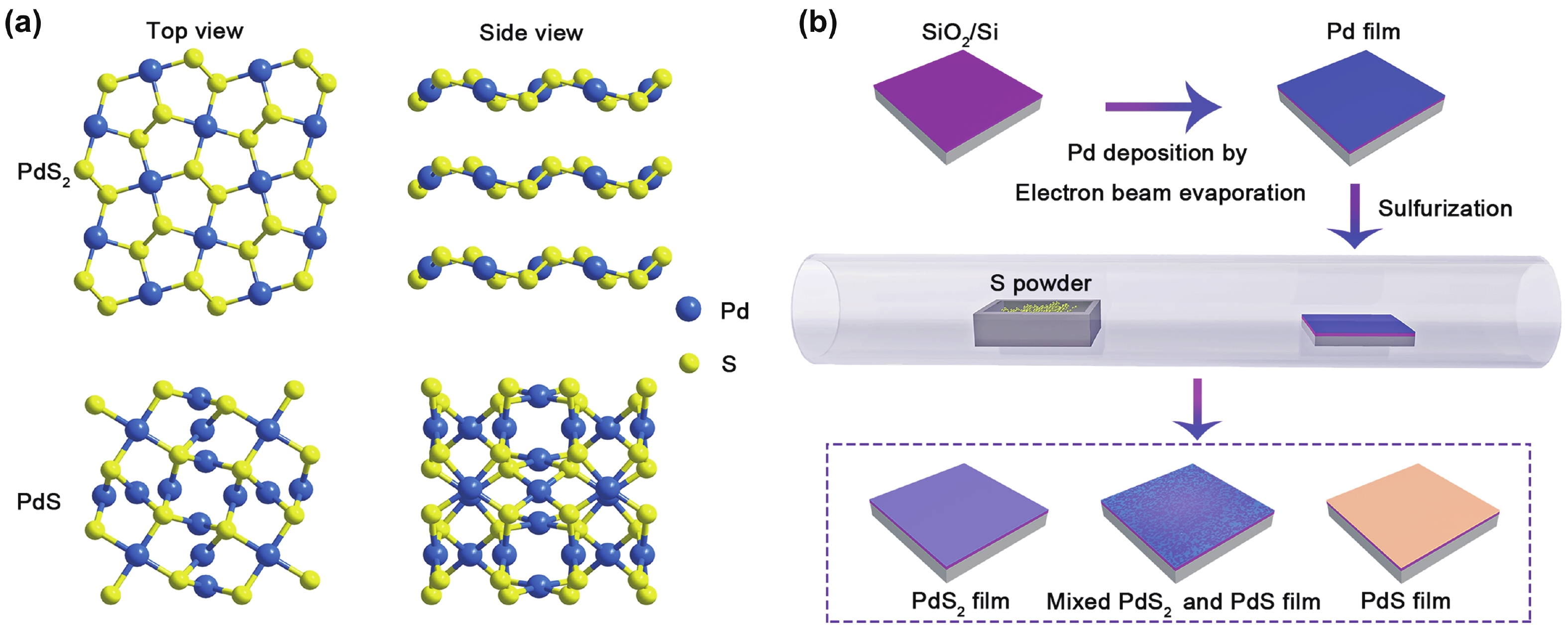
(Color online) (a) Side and top views of the schematic crystal structures for PdS2 and PdS. (b) Schematic for the synthesis of PdS and PdS2 NFs.
ARTICLES
Hui Gao1, §, Hongyi Zhou1, §, Yulong Hao2, §, Guoliang Zhou3, Huan Zhou1, Fenglin Gao1, Jinbiao Xiao1, Pinghua Tang1 and Guolin Hao1, 4,
Corresponding author: Guolin Hao, guolinhao@xtu.edu.cn
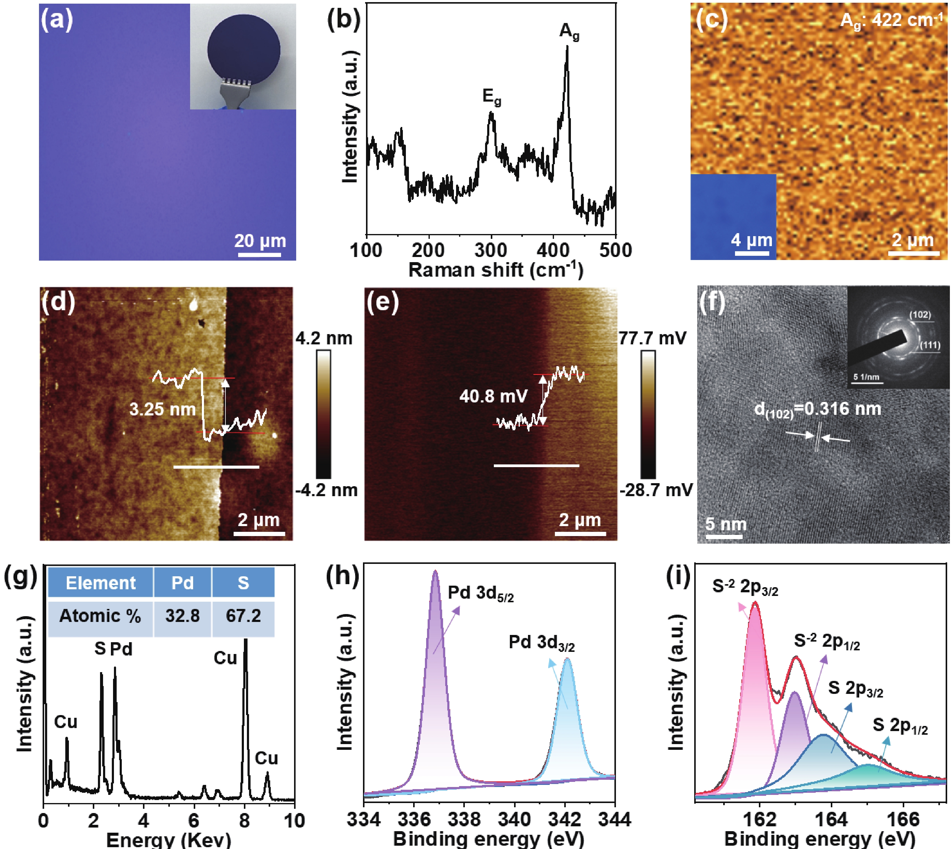
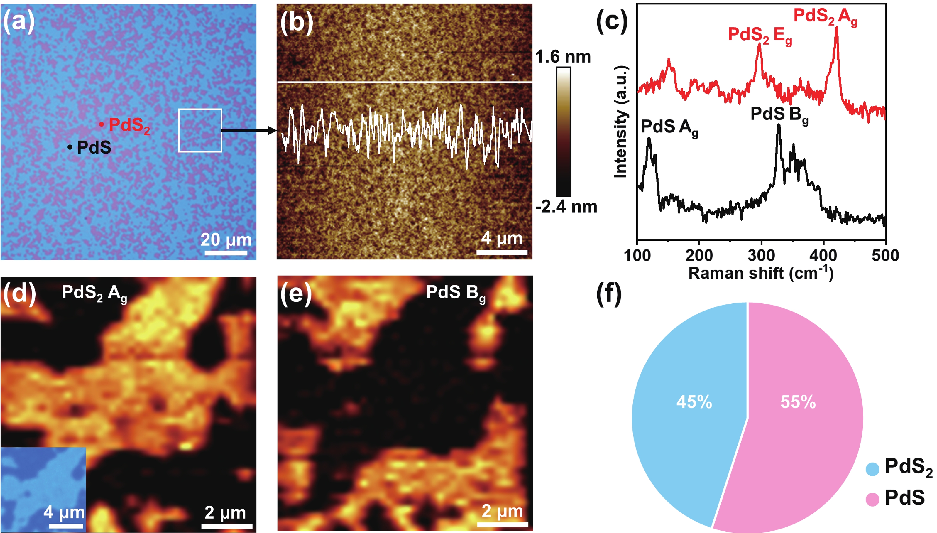
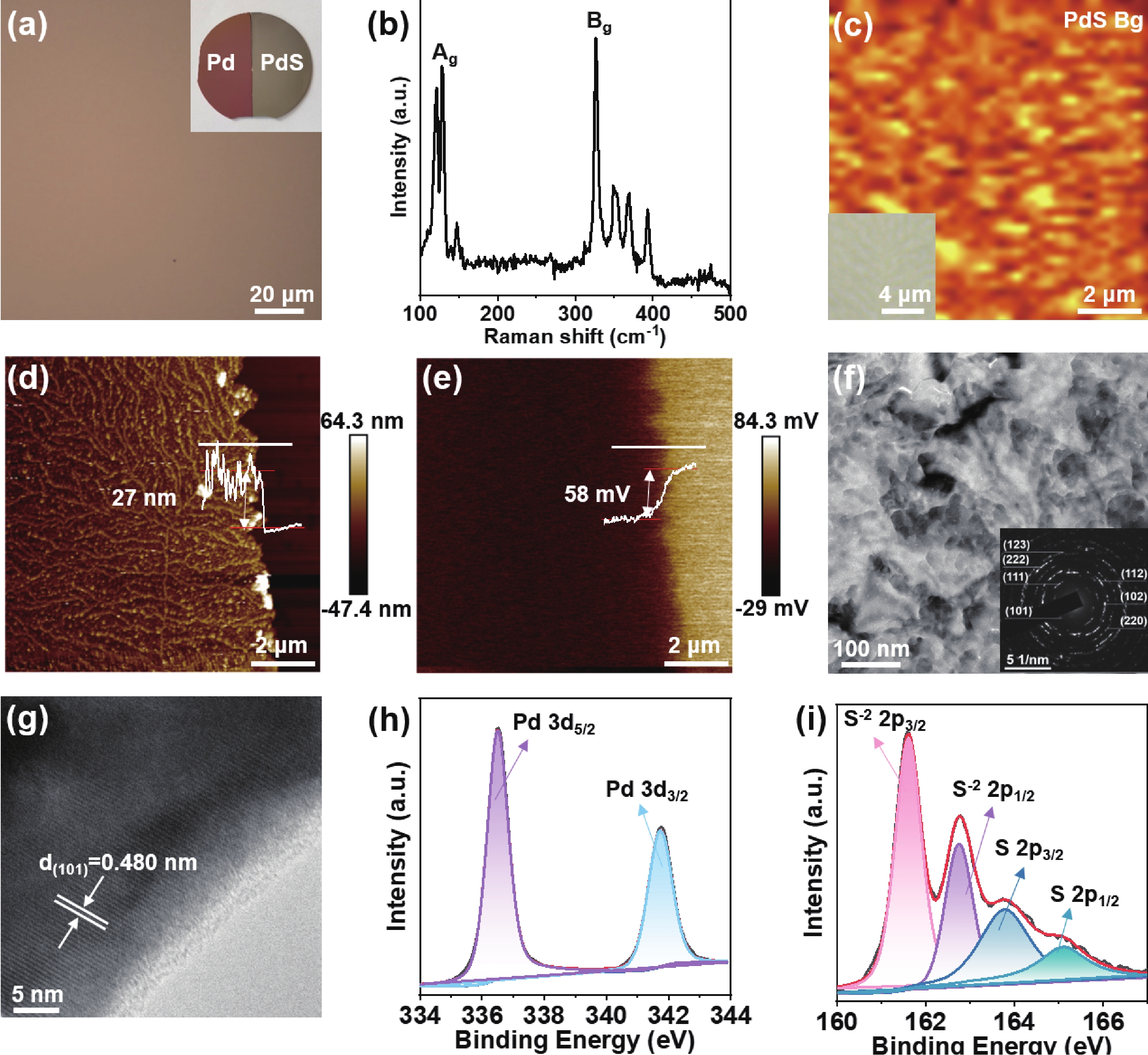
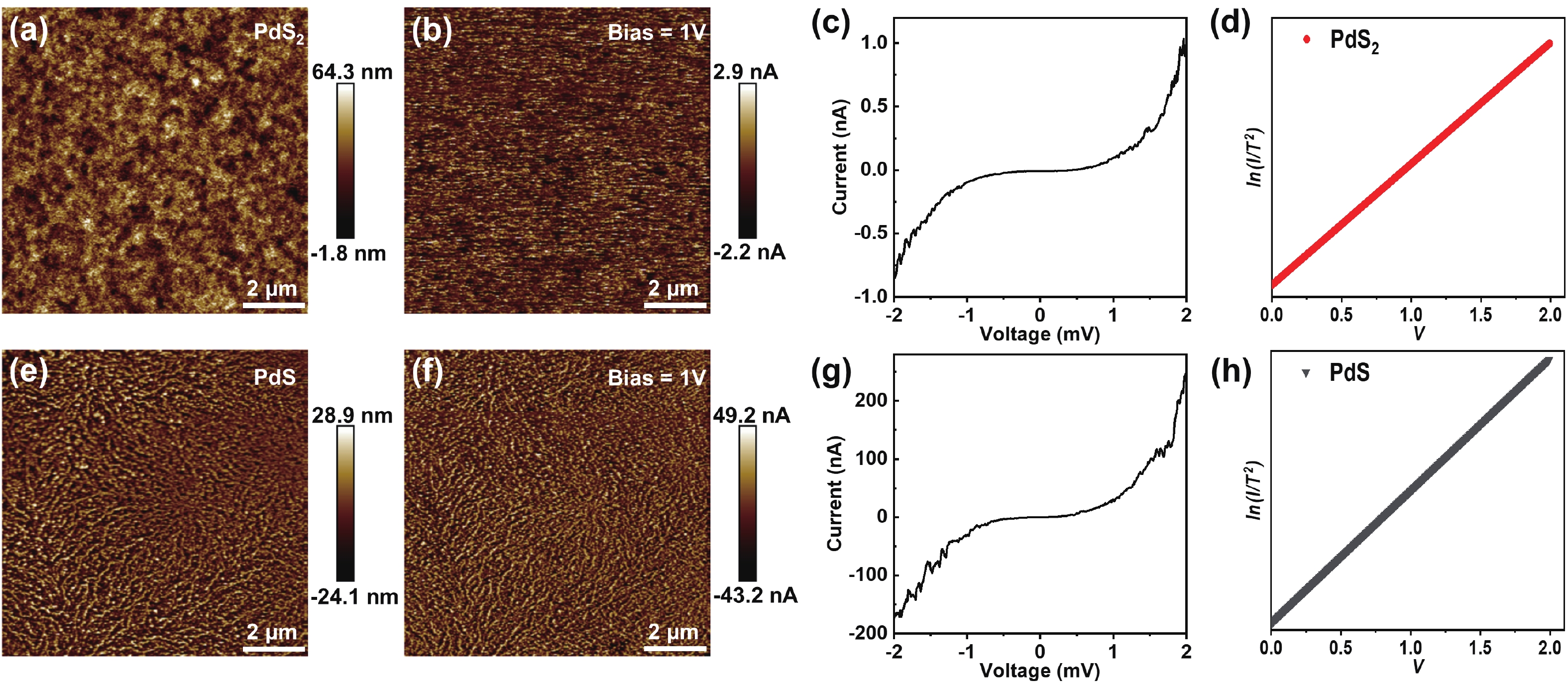
Abstract: Palladium (Pd)-based sulfides have triggered extensive interest due to their unique properties and potential applications in the fields of electronics and optoelectronics. However, the synthesis of large-scale uniform PdS and PdS2 nanofilms (NFs) remains an enormous challenge. In this work, 2-inch wafer-scale PdS and PdS2 NFs with excellent stability can be controllably prepared via chemical vapor deposition combined with electron beam evaporation technique. The thickness of the pre-deposited Pd film and the sulfurization temperature are critical for the precise synthesis of PdS and PdS2 NFs. A corresponding growth mechanism has been proposed based on our experimental results and Gibbs free energy calculations. The electrical transport properties of PdS and PdS2 NFs were explored by conductive atomic force microscopy. Our findings have achieved the controllable growth of PdS and PdS2 NFs, which may provide a pathway to facilitate PdS and PdS2 based applications for next-generation high performance optoelectronic devices.
Key words: PdS, PdS2, nanofilms, controllable growth, chemical vapor deposition, electron beam evaporation
| [1] |
Novoselov K S, Geim A K, Morozov S V, et al. Electric field effect in atomically thin carbon films. Science, 2004, 306, 666 doi: 10.1126/science.1102896
|
| [2] |
Wang Q H, Kalantar-Zadeh K, Kis A, et al. Electronics and optoelectronics of two-dimensional transition metal dichalcogenides. Nat Nanotechnol, 2012, 7, 699 doi: 10.1038/nnano.2012.193
|
| [3] |
Chen T, Hao G L, Wang G, et al. Controlled growth of atomically thin MoSe2 films and nanoribbons by chemical vapor deposition. 2D Mater, 2019, 6, 025002 doi: 10.1088/2053-1583/aaf9cc
|
| [4] |
Duan Z J, Chen T, Shi J W, et al. Space-confined and substrate-directed synthesis of transition-metal dichalcogenide nanostructures with tunable dimensionality. Sci Bull, 2020, 65, 1013 doi: 10.1016/j.scib.2020.03.002
|
| [5] |
Kempt R, Kuc A, Heine T. Two-dimensional noble-metal chalcogenides and phosphochalcogenides. Angew Chem Int Ed, 2020, 59, 9242 doi: 10.1002/anie.201914886
|
| [6] |
Miró P, Ghorbani-Asl M, Heine T. Two dimensional materials beyond MoS2: Noble-transition-metal dichalcogenides. Angew Chem Int Ed, 2014, 53, 3015 doi: 10.1002/anie.201309280
|
| [7] |
Wang Y, Li Y F, Chen Z F. Not your familiar two dimensional transition metal disulfide: Structural and electronic properties of the PdS2 monolayer. J Mater Chem C, 2015, 3, 9603 doi: 10.1039/C5TC01345C
|
| [8] |
Wang Y W, Zhou L, Zhong M Z, et al. Two-dimensional noble transition-metal dichalcogenides for nanophotonics and optoelectronics: Status and prospects. Nano Res, 2022, 15, 3675 doi: 10.1007/s12274-021-3979-6
|
| [9] |
Song S, Sim Y, Kim S Y, et al. Wafer-scale production of patterned transition metal ditelluride layers for two-dimensional metal–semiconductor contacts at the Schottky–Mott limit. Nat Electron, 2020, 3, 207 doi: 10.1038/s41928-020-0396-x
|
| [10] |
Cheng P K, Liu S X, Ahmed S, et al. Ultrafast Yb-doped fiber laser using few layers of PdS2 saturable absorber. Nanomaterials, 2020, 10, 2441 doi: 10.3390/nano10122441
|
| [11] |
Cheng P K, Tang C Y, Wang X Y, et al. Passively Q-switched and femtosecond mode-locked erbium-doped fiber laser based on a 2D palladium disulfide (PdS2) saturable absorber. Photon Res, 2020, 8, 511 doi: 10.1364/PRJ.380146
|
| [12] |
Ghorbani-Asl M, Kuc A, Miró P, et al. A single-material logical junction based on 2D crystal PdS2. Adv Mater, 2016, 28, 853 doi: 10.1002/adma.201504274
|
| [13] |
Zhang X D, Su G W, Lu J W, et al. Centimeter-scale few-layer PdS2: Fabrication and physical properties. ACS Appl Mater Interfaces, 2021, 13, 43063 doi: 10.1021/acsami.1c11824
|
| [14] |
He K, Xu W T, Tang J M, et al. Centimeter-scale PdS2 ultrathin films with high mobility and broadband photoresponse. Small, 2023, 19, 2206915 doi: 10.1002/smll.202206915
|
| [15] |
Lan Y S, Chen X R, Hu C E, et al. Penta-PdX2 (X = S, Se, Te) monolayers: Promising anisotropic thermoelectric materials. J Mater Chem A, 2019, 7, 11134 doi: 10.1039/C9TA02138H
|
| [16] |
Figueiredo R O, Seixas L. Hydrogen-evolution reaction in two-dimensional PdS2 by phase and defect engineering. Phys Rev Applied, 2022, 17, 034035 doi: 10.1103/PhysRevApplied.17.034035
|
| [17] |
Guha A K, Sharma R, Sahoo K R, et al. One-dimensional hollow structures of 2O-PdS2 decorated carbon for water electrolysis. ACS Appl Energy Mater, 2021, 4, 8715 doi: 10.1021/acsaem.1c01703
|
| [18] |
ElGhazali M A, Naumov P G, Mu Q, et al. Pressure-induced metallization, transition to the pyrite-type structure, and superconductivity in palladium disulfide PdS2. Phys Rev B, 2019, 100, 014507 doi: 10.1103/PhysRevB.100.014507
|
| [19] |
Zheng J Y, Miao T T, Xu R, et al. Chemical synthesis and integration of Highly conductive PdTe2 with low-dimensional semiconductors for p-type transistors with low contact barriers. Adv Mater, 2021, 33, 2101150 doi: 10.1002/adma.202101150
|
| [20] |
Wang Y H, Zhang Y H, Cheng Q L, et al. Large area uniform PtSx synthesis on sapphire substrate for performance improved photodetectors. Appl Mater Today, 2021, 25, 101176 doi: 10.1016/j.apmt.2021.101176
|
| [21] |
Zhang K N, Wang M, Zhou X, et al. Growth of large scale PtTe, PtTe2 and PtSe2 films on a wide range of substrates. Nano Res, 2021, 14, 1663 doi: 10.1007/s12274-020-2942-2
|
| [22] |
Ferrer I J, Díaz-Chao P, Pascual A, et al. An investigation on palladium sulphide (PdS) thin films as a photovoltaic material. Thin Solid Films, 2007, 515, 5783 doi: 10.1016/j.tsf.2006.12.079
|
| [23] |
Barawi M, Ferrer I J, Ares J R, et al. Hydrogen evolution using palladium sulfide (PdS) nanocorals as photoanodes in aqueous solution. ACS Appl Mater Interfaces, 2014, 6, 20544 doi: 10.1021/am5061504
|
| [24] |
Chen L C, Jiang B B, Yu H, et al. Thermoelectric properties of polycrystalline palladium sulfide. RSC Adv, 2018, 8, 13154 doi: 10.1039/C8RA01613E
|
| [25] |
Folmer J C W, Turner J A, Parkinson B A. Photoelectrochemical characterization of several semiconducting compounds of palladium with sulfur and/or phosphorus. J Solid State Chem, 1987, 68, 28 doi: 10.1016/0022-4596(87)90281-7
|
| [26] |
Sun G T, Mao S M, Ma D D, et al. One-step vulcanization of Cd(OH)Cl nanorods to synthesize CdS/ZnS/PdS nanotubes for highly efficient photocatalytic hydrogen evolution. J Mater Chem A, 2019, 7, 15278 doi: 10.1039/C9TA03862K
|
| [27] |
Li Y, Yu S, Xiang J L, et al. Revealing the importance of hole transfer: Boosting photocatalytic hydrogen evolution by delicate modulation of photogenerated holes. ACS Catal, 2023, 13, 8281 doi: 10.1021/acscatal.3c01210
|
| [28] |
Bhatt R, Bhattacharya S, Basu R, et al. Growth of Pd4S, PdS and PdS2 films by controlled sulfurization of sputtered Pd on native oxide of Si. Thin Solid Films, 2013, 539, 41 doi: 10.1016/j.tsf.2013.04.143
|
| [29] |
Zhao D H, Xie S, Wang Y, et al. Synthesis of large-scale few-layer PtS2 films by chemical vapor deposition. AIP Adv, 2019, 9, 025225 doi: 10.1063/1.5086447
|
| [30] |
Chen L C, Cao Z Y, Yu H, et al. Phonon anharmonicity in thermoelectric palladium sulfide by Raman spectroscopy. Appl Phys Lett, 2018, 113, 022105 doi: 10.1063/1.5041973
|
| [31] |
Chen L C, Peng Q, Yu H, et al. Lattice dynamics of thermoelectric palladium sulfide. J Alloys Compd, 2019, 798, 484 doi: 10.1016/j.jallcom.2019.05.280
|
| [32] |
Diaz-Chao P, Ferrer I J, Ares J R, et al. Cubic Pd16S7 as a precursor phase in the formation of tetragonal PdS by sulfuration of Pd thin films. J Phys Chem C, 2009, 113, 5329 doi: 10.1021/jp810631t
|
| [33] |
Li Y, Xu C Y, Zhen L. Surface potential and interlayer screening effects of few-layer MoS2 nanoflakes. Appl Phys Lett, 2013, 102, 143110 doi: 10.1063/1.4801844
|
| [34] |
Khan A R, Lu T, Ma W D, et al. Tunable optoelectronic properties of WS2 by local strain engineering and folding. Adv Electron Mater, 2020, 6, 1901381 doi: 10.1002/aelm.201901381
|
| [35] |
Ali S M, AlGarawi M S, Khan S U D, et al. Nanostructure, optical and electrical response of gamma ray radiated PdS/p-Si heterojunction. Mater Sci Semicond Process, 2021, 122, 105474 doi: 10.1016/j.mssp.2020.105474
|


Article views: 588 Times PDF downloads: 97 Times Cited by: 0 Times
Received: 11 June 2023 Revised: 12 July 2023 Online: Accepted Manuscript: 08 September 2023Uncorrected proof: 21 November 2023Published: 10 December 2023
| Citation: |
Hui Gao, Hongyi Zhou, Yulong Hao, Guoliang Zhou, Huan Zhou, Fenglin Gao, Jinbiao Xiao, Pinghua Tang, Guolin Hao. Controllable growth of wafer-scale PdS and PdS2 nanofilms via chemical vapor deposition combined with an electron beam evaporation technique[J]. Journal of Semiconductors, 2023, 44(12): 122001. doi: 10.1088/1674-4926/44/12/122001
H Gao, H Y Zhou, Y L Hao, G L Zhou, H Zhou, F L Gao, J B Xiao, P H Tang, G L Hao. Controllable growth of wafer-scale PdS and PdS2 nanofilms via chemical vapor deposition combined with an electron beam evaporation technique[J]. J. Semicond, 2023, 44(12): 122001. doi: 10.1088/1674-4926/44/12/122001
Export: BibTex EndNote

|
| [1] |
Novoselov K S, Geim A K, Morozov S V, et al. Electric field effect in atomically thin carbon films. Science, 2004, 306, 666 doi: 10.1126/science.1102896
|
| [2] |
Wang Q H, Kalantar-Zadeh K, Kis A, et al. Electronics and optoelectronics of two-dimensional transition metal dichalcogenides. Nat Nanotechnol, 2012, 7, 699 doi: 10.1038/nnano.2012.193
|
| [3] |
Chen T, Hao G L, Wang G, et al. Controlled growth of atomically thin MoSe2 films and nanoribbons by chemical vapor deposition. 2D Mater, 2019, 6, 025002 doi: 10.1088/2053-1583/aaf9cc
|
| [4] |
Duan Z J, Chen T, Shi J W, et al. Space-confined and substrate-directed synthesis of transition-metal dichalcogenide nanostructures with tunable dimensionality. Sci Bull, 2020, 65, 1013 doi: 10.1016/j.scib.2020.03.002
|
| [5] |
Kempt R, Kuc A, Heine T. Two-dimensional noble-metal chalcogenides and phosphochalcogenides. Angew Chem Int Ed, 2020, 59, 9242 doi: 10.1002/anie.201914886
|
| [6] |
Miró P, Ghorbani-Asl M, Heine T. Two dimensional materials beyond MoS2: Noble-transition-metal dichalcogenides. Angew Chem Int Ed, 2014, 53, 3015 doi: 10.1002/anie.201309280
|
| [7] |
Wang Y, Li Y F, Chen Z F. Not your familiar two dimensional transition metal disulfide: Structural and electronic properties of the PdS2 monolayer. J Mater Chem C, 2015, 3, 9603 doi: 10.1039/C5TC01345C
|
| [8] |
Wang Y W, Zhou L, Zhong M Z, et al. Two-dimensional noble transition-metal dichalcogenides for nanophotonics and optoelectronics: Status and prospects. Nano Res, 2022, 15, 3675 doi: 10.1007/s12274-021-3979-6
|
| [9] |
Song S, Sim Y, Kim S Y, et al. Wafer-scale production of patterned transition metal ditelluride layers for two-dimensional metal–semiconductor contacts at the Schottky–Mott limit. Nat Electron, 2020, 3, 207 doi: 10.1038/s41928-020-0396-x
|
| [10] |
Cheng P K, Liu S X, Ahmed S, et al. Ultrafast Yb-doped fiber laser using few layers of PdS2 saturable absorber. Nanomaterials, 2020, 10, 2441 doi: 10.3390/nano10122441
|
| [11] |
Cheng P K, Tang C Y, Wang X Y, et al. Passively Q-switched and femtosecond mode-locked erbium-doped fiber laser based on a 2D palladium disulfide (PdS2) saturable absorber. Photon Res, 2020, 8, 511 doi: 10.1364/PRJ.380146
|
| [12] |
Ghorbani-Asl M, Kuc A, Miró P, et al. A single-material logical junction based on 2D crystal PdS2. Adv Mater, 2016, 28, 853 doi: 10.1002/adma.201504274
|
| [13] |
Zhang X D, Su G W, Lu J W, et al. Centimeter-scale few-layer PdS2: Fabrication and physical properties. ACS Appl Mater Interfaces, 2021, 13, 43063 doi: 10.1021/acsami.1c11824
|
| [14] |
He K, Xu W T, Tang J M, et al. Centimeter-scale PdS2 ultrathin films with high mobility and broadband photoresponse. Small, 2023, 19, 2206915 doi: 10.1002/smll.202206915
|
| [15] |
Lan Y S, Chen X R, Hu C E, et al. Penta-PdX2 (X = S, Se, Te) monolayers: Promising anisotropic thermoelectric materials. J Mater Chem A, 2019, 7, 11134 doi: 10.1039/C9TA02138H
|
| [16] |
Figueiredo R O, Seixas L. Hydrogen-evolution reaction in two-dimensional PdS2 by phase and defect engineering. Phys Rev Applied, 2022, 17, 034035 doi: 10.1103/PhysRevApplied.17.034035
|
| [17] |
Guha A K, Sharma R, Sahoo K R, et al. One-dimensional hollow structures of 2O-PdS2 decorated carbon for water electrolysis. ACS Appl Energy Mater, 2021, 4, 8715 doi: 10.1021/acsaem.1c01703
|
| [18] |
ElGhazali M A, Naumov P G, Mu Q, et al. Pressure-induced metallization, transition to the pyrite-type structure, and superconductivity in palladium disulfide PdS2. Phys Rev B, 2019, 100, 014507 doi: 10.1103/PhysRevB.100.014507
|
| [19] |
Zheng J Y, Miao T T, Xu R, et al. Chemical synthesis and integration of Highly conductive PdTe2 with low-dimensional semiconductors for p-type transistors with low contact barriers. Adv Mater, 2021, 33, 2101150 doi: 10.1002/adma.202101150
|
| [20] |
Wang Y H, Zhang Y H, Cheng Q L, et al. Large area uniform PtSx synthesis on sapphire substrate for performance improved photodetectors. Appl Mater Today, 2021, 25, 101176 doi: 10.1016/j.apmt.2021.101176
|
| [21] |
Zhang K N, Wang M, Zhou X, et al. Growth of large scale PtTe, PtTe2 and PtSe2 films on a wide range of substrates. Nano Res, 2021, 14, 1663 doi: 10.1007/s12274-020-2942-2
|
| [22] |
Ferrer I J, Díaz-Chao P, Pascual A, et al. An investigation on palladium sulphide (PdS) thin films as a photovoltaic material. Thin Solid Films, 2007, 515, 5783 doi: 10.1016/j.tsf.2006.12.079
|
| [23] |
Barawi M, Ferrer I J, Ares J R, et al. Hydrogen evolution using palladium sulfide (PdS) nanocorals as photoanodes in aqueous solution. ACS Appl Mater Interfaces, 2014, 6, 20544 doi: 10.1021/am5061504
|
| [24] |
Chen L C, Jiang B B, Yu H, et al. Thermoelectric properties of polycrystalline palladium sulfide. RSC Adv, 2018, 8, 13154 doi: 10.1039/C8RA01613E
|
| [25] |
Folmer J C W, Turner J A, Parkinson B A. Photoelectrochemical characterization of several semiconducting compounds of palladium with sulfur and/or phosphorus. J Solid State Chem, 1987, 68, 28 doi: 10.1016/0022-4596(87)90281-7
|
| [26] |
Sun G T, Mao S M, Ma D D, et al. One-step vulcanization of Cd(OH)Cl nanorods to synthesize CdS/ZnS/PdS nanotubes for highly efficient photocatalytic hydrogen evolution. J Mater Chem A, 2019, 7, 15278 doi: 10.1039/C9TA03862K
|
| [27] |
Li Y, Yu S, Xiang J L, et al. Revealing the importance of hole transfer: Boosting photocatalytic hydrogen evolution by delicate modulation of photogenerated holes. ACS Catal, 2023, 13, 8281 doi: 10.1021/acscatal.3c01210
|
| [28] |
Bhatt R, Bhattacharya S, Basu R, et al. Growth of Pd4S, PdS and PdS2 films by controlled sulfurization of sputtered Pd on native oxide of Si. Thin Solid Films, 2013, 539, 41 doi: 10.1016/j.tsf.2013.04.143
|
| [29] |
Zhao D H, Xie S, Wang Y, et al. Synthesis of large-scale few-layer PtS2 films by chemical vapor deposition. AIP Adv, 2019, 9, 025225 doi: 10.1063/1.5086447
|
| [30] |
Chen L C, Cao Z Y, Yu H, et al. Phonon anharmonicity in thermoelectric palladium sulfide by Raman spectroscopy. Appl Phys Lett, 2018, 113, 022105 doi: 10.1063/1.5041973
|
| [31] |
Chen L C, Peng Q, Yu H, et al. Lattice dynamics of thermoelectric palladium sulfide. J Alloys Compd, 2019, 798, 484 doi: 10.1016/j.jallcom.2019.05.280
|
| [32] |
Diaz-Chao P, Ferrer I J, Ares J R, et al. Cubic Pd16S7 as a precursor phase in the formation of tetragonal PdS by sulfuration of Pd thin films. J Phys Chem C, 2009, 113, 5329 doi: 10.1021/jp810631t
|
| [33] |
Li Y, Xu C Y, Zhen L. Surface potential and interlayer screening effects of few-layer MoS2 nanoflakes. Appl Phys Lett, 2013, 102, 143110 doi: 10.1063/1.4801844
|
| [34] |
Khan A R, Lu T, Ma W D, et al. Tunable optoelectronic properties of WS2 by local strain engineering and folding. Adv Electron Mater, 2020, 6, 1901381 doi: 10.1002/aelm.201901381
|
| [35] |
Ali S M, AlGarawi M S, Khan S U D, et al. Nanostructure, optical and electrical response of gamma ray radiated PdS/p-Si heterojunction. Mater Sci Semicond Process, 2021, 122, 105474 doi: 10.1016/j.mssp.2020.105474
|
 23060015.pdf
|

|

 WeChat ID
Journal of Semiconductors © 2017 All Rights Reserved 京ICP备05085259号-2

 DownLoad:

