ARTICLES

Demonstration of a manufacturable SOT-MRAM multiplexer array towards industrial applications

Chuanpeng Jiang1, Jinhao Li1, Hongchao Zhang1, Shiyang Lu1, Pengbin Li1, Chao Wang1, Zhongkui Zhang1, Zhengyi Hou1, Xu Liu1, Jiagao Feng1, He Zhang1, Hui Jin1, Gefei Wang2, Hongxi Liu2, , Kaihua Cao2, , Zhaohao Wang1, and Weisheng Zhao1

+ Author Affiliations

 Corresponding author: Hongxi Liu, hongxi_liu@tmc-bj.cn; Kaihua Cao, kaihua_cao@tmc-bj.cn; Zhaohao Wang, zhaohao.wang@buaa.edu.cn

PDF

Turn off MathJax

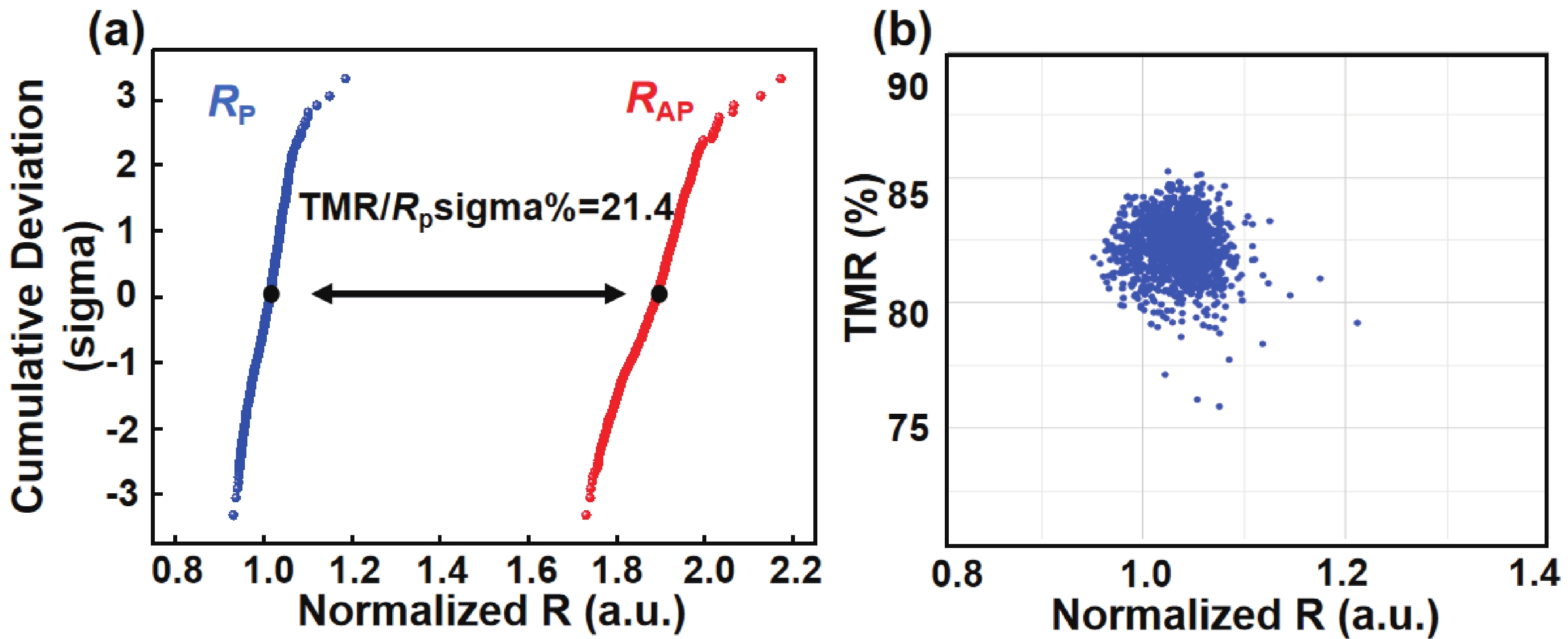
Abstract: We have successfully demonstrated a 1 Kb spin-orbit torque (SOT) magnetic random-access memory (MRAM) multiplexer (MUX) array with remarkable performance. The 1 Kb MUX array exhibits an in-die function yield of over 99.6%. Additionally, it provides a sufficient readout window, with a TMR/RP_sigma% value of 21.4. Moreover, the SOT magnetic tunnel junctions (MTJs) in the array show write error rates as low as 10−6 without any ballooning effects or back-hopping behaviors, ensuring the write stability and reliability. This array achieves write operations in 20 ns and 1.2 V for an industrial-level temperature range from −40 to 125 °C. Overall, the demonstrated array shows competitive specifications compared to the state-of-the-art works. Our work paves the way for the industrial-scale production of SOT-MRAM, moving this technology beyond R&D and towards widespread adoption.

Key words: spin-orbit torqueMRAMmultiplexer array200 mm-wafer platformstabilityreliability


[1]
Clarke P. TSMC embedded MRAM is key to Gyrfalcon AI chip. Technology News, 2018, [2018-9-22]. https://www.eenewseurope.com/
[2]
Choe J. TSMC 22ULL eMRAM Die removed from Ambiq Apollo-4, Another Disruptive Technology on Embedded Memory. TechInsights TechStream Blog_Emerging Memory, 2021 [2021-8-13]. https://www.techinsights.com/
[3]
Choe J. Recent technology insights on STT-MRAM: Structure, materials, and process integration. 2023 IEEE International Memory Workshop (IMW), Monterey, 2023, 1 doi: 10.1109/IMW56887.2023.10145822
[4]
Chiang H L, Wang J F, Chen T C, et al. Cold MRAM as a density booster for embedded NVM in advanced technology. 2021 Symposium on VLSI Technology, 2021, 1
[5]
Chen C H, Chang C Y, Weng C H, et al. Reliability and magnetic immunity of reflow-capable embedded STT-MRAM in 16nm FinFET CMOS process. 2021 Symposium on VLSI Technology, 2021, 1
[6]
Wang C Y, Shih M C, Weng C H, et al. Reliability demonstration of reflow qualified 22nm STT-MRAM for embedded memory applications. 2020 IEEE Symposium on VLSI Technology, 2020, 1 doi: 10.1109/VLSITechnology18217.2020.9265054
[7]
Lee K, Yamane K, Noh S, et al. 22-nm FD-SOI embedded MRAM with full solder reflow compatibility and enhanced magnetic immunity. 2018 IEEE Symposium on VLSI Technology, 2018, 183 doi: 10.1109/VLSIT.2018.8510655
[8]
Naik V B, Lee K, Yamane K, et al. Manufacturable 22nm FD-SOI embedded MRAM technology for industrial-grade MCU and IOT applications. 2019 IEEE International Electron Devices Meeting (IEDM), 2019, 2.3.1 doi: 10.1109/IEDM19573.2019.8993454
[9]
Naik V B, Yamane K, Kwon J, et al. STT-MRAM: A robust embedded non-volatile memory with superior reliability and immunity to external magnetic field and RF sources. Proceedings of 2021 IEEE Symposium on VLSI Technology, 2021, 1
[10]
Naik V B, Yamane K, Lee T Y, et al. JEDEC-qualified highly reliable 22nm FD-SOI embedded MRAM for low-power industrial-grade, and extended performance towards automotive-grade-1 applications. 2020 IEEE International Electron Devices Meeting (IEDM), 2021, 11.3.1 doi: 10.1109/IEDM13553.2020.9371935
[11]
Lee K, Bak J H, Kim Y J, et al. 1Gbit high density embedded STT-MRAM in 28nm FDSOI technology. 2019 IEEE International Electron Devices Meeting (IEDM), 2019, 2.2.1 doi: 10.1109/IEDM19573.2019.8993551
[12]
Lee K, Kim D S, Bak J H, et al. 28nm CIS-compatible embedded STT-MRAM for frame buffer memory. 2021 IEEE International Electron Devices Meeting (IEDM), 2021, 2.1.1 doi: 10.1109/IEDM19574.2021.9720537
[13]
Suh K, Lee J H, Shin H M, et al. 12.5 Mb/mm2 embedded MRAM for high density non-volatile RAM applications. 2021 Symposium on VLSI Technology, 2021, 1
[14]
Endoh T, Honjo H, Nishioka K, et al. Recent progresses in STT-MRAM and SOT-MRAM for next generation MRAM. 2020 IEEE Symposium on VLSI Technology, 2020, 1 doi: 10.1109/VLSITechnology18217.2020.9265042
[15]
Rao S, Kim W, van Beek S, et al. STT-MRAM array performance improvement through optimization of Ion beam etch and MTJ for last-level cache application. 2021 IEEE International Memory Workshop (IMW), 2021, 1 doi: 10.1109/IMW51353.2021.9439592
[16]
Wu H, Katragadda V, Evarts E, et al. First experimental demonstration of MRAM data scrubbing: 80 Mb MRAM with 40 nm junctions for last level cache applications. 2021 IEEE International Electron Devices Meeting (IEDM), 2021, 2.3.1 doi: 10.1109/IEDM19574.2021.9720539
[17]
Edelstein D, Rizzolo M, Sil D, et al. A 14 nm embedded STT-MRAM CMOS technology. 2020 IEEE International Electron Devices Meeting (IEDM), 2020, 11.5.1 doi: 10.1109/IEDM13553.2020.9371922
[18]
Worledge D C. Spin-transfer-torque MRAM: The next revolution in memory. 2022 IEEE International Memory Workshop (IMW), 2022, 1 doi: 10.1109/IMW52921.2022.9779288
[19]
Mihai Miron I, Gaudin G, Auffret S, et al. Current-driven spin torque induced by the Rashba effect in a ferromagnetic metal layer. Nat Mater, 2010, 9, 230 doi: 10.1038/nmat2613
[20]
Miron I M, Garello K, Gaudin G, et al. Perpendicular switching of a single ferromagnetic layer induced by in-plane current injection. Nature, 2011, 476, 189 doi: 10.1038/nature10309
[21]
Cubukcu M, Boulle O, Drouard M, et al. Spin-orbit torque magnetization switching of a three-terminal perpendicular magnetic tunnel junction. Appl Phys Lett, 2014, 104, 042406 doi: 10.1063/1.4863407
[22]
Liu L Q, Lee O J, Gudmundsen T J, et al. Current-induced switching of perpendicularly magnetized magnetic layers using spin torque from the spin Hall effect. Phys Rev Lett, 2012, 109, 096602 doi: 10.1103/PhysRevLett.109.096602
[23]
Liu L Q, Pai C F, Li Y, et al. Spin-torque switching with the giant spin Hall effect of tantalum. Science, 2012, 336, 555 doi: 10.1126/science.1218197
[24]
Pai C F, Liu L Q, Li Y, et al. Spin transfer torque devices utilizing the giant spin Hall effect of tungsten. Appl Phys Lett, 2012, 101, 122404 doi: 10.1063/1.4753947
[25]
Shao Q M, Li P, Liu L Q, et al. Roadmap of spin–orbit torques. IEEE Trans Magn, 2021, 57, 1 doi: 10.1109/TMAG.2021.3078583
[26]
Guo Z X, Yin J L, Bai Y, et al. Spintronics for energy- efficient computing: An overview and outlook. Proc IEEE, 2021, 109, 1398 doi: 10.1109/JPROC.2021.3084997
[27]
Van Beek S, Cai K M, Fan K Q, et al. MTJ degradation in multi-pillar SOT-MRAM with selective writing. 2023 IEEE International Reliability Physics Symposium (IRPS), 2023, 1 doi: MTJdegradationinmulti-pil-larSOT-MRAMwithselectivewriting
[28]
Xu X Y, Zhang H C, Jiang C P, et al. Full reliability characterization of three-terminal SOT-MTJ devices and corresponding arrays. 2023 IEEE International Reliability Physics Symposium (IRPS), 2023, 1 doi: 10.1109/IRPS48203.2023.10117643
[29]
Sverdlov V, Makarov A, Selberherr S. Two-pulse sub-ns switching scheme for advanced spin-orbit torque MRAM. Solid State Electron, 2019, 155, 49 doi: 10.1016/j.sse.2019.03.010
[30]
Lee K S, Lee S W, Min B C, et al. Threshold current for switching of a perpendicular magnetic layer induced by spin Hall effect. Appl Phys Lett, 2013, 102, 112410 doi: 10.1063/1.4798288
[31]
Liu H, Bedau D, Sun J Z, et al. Dynamics of spin torque switching in all-perpendicular spin valve nanopillars. J Magn Magn Mater, 2014, 358, 233 doi: 10.1016/j.jmmm.2014.01.061
[32]
Wang M X, Cai W L, Zhu D Q, et al. Field-free switching of a perpendicular magnetic tunnel junction through the interplay of spin-orbit and spin-transfer torques. Nat Electron, 2018, 1, 582 doi: 10.1038/s41928-018-0160-7
[33]
Garello K, Yasin F, Couet S, et al. SOT-MRAM 300MM integration for low power and ultrafast embedded memories. 2018 IEEE Symposium on VLSI Circuits, 2018, 81 doi: 10.1109/VLSIC.2018.8502269
[34]
Garello K, Yasin F, Hody H, et al. Manufacturable 300mm platform solution for field-free switching SOT-MRAM. 2019 Symposium on VLSI Circuits, 2019, T194 doi: 10.23919/VLSIC.2019.8778100
[35]
Honjo H, Nguyen T V A, Watanabe T, et al. First demonstration of field-free SOT-MRAM with 0.35 ns write speed and 70 thermal stability under 400°C thermal tolerance by canted SOT structure and its advanced patterning/SOT channel technology. 2019 IEEE International Electron Devices Meeting (IEDM), 2020, 28.5.1 doi: 10.1109/IEDM19573.2019.8993443
[36]
Wu Y C, Kim W, Garello K, et al. Deterministic and field-free voltage-controlled MRAM for high performance and low power applications. 2020 IEEE Symposium on VLSI Technology, 2020, 1 doi: 10.1109/VLSITechnology18217.2020.9265057
[37]
Natsui M, Tamakoshi A, Honjo H, et al. Dual-port SOT-MRAM achieving 90-MHz read and 60-MHz write operations under field-assistance-free condition. IEEE J Solid-State Circuits, 2021, 56, 1116 doi: 10.1109/JSSC.2020.3039800
[38]
Chen G L, Wang I J, Yeh P S, et al. An 8kb spin-orbit-torque magnetic random-access memory. 2021 International Symposium on VLSI Technology, Systems and Applications (VLSI-TSA), 2021, 1 doi: 10.1109/VLSI-TSA51926.2021.9440096
[39]
Song M Y, Lee C M, Yang S Y, et al. High speed (1ns) and low voltage (1.5V) demonstration of 8Kb SOT-MRAM array. 2022 IEEE Symposium on VLSI Technology and Circuits (VLSI Technology and Circuits), 2022, 377 doi: 10.1109/VLSITechnologyandCir46769.2022.9830149
[40]
Couet S, Rao S, Van Beek S, et al. BEOL compatible high retention perpendicular SOT-MRAM device for SRAM replacement and machine learning. 2021 Symposium on VLSI Technology, 2021, 1
[41]
Zhu D Q, Guo Z X, Du A, et al. First demonstration of three terminal MRAM devices with immunity to magnetic fields and 10 ns field free switching by electrical manipulation of exchange bias. 2021 IEEE International Electron Devices Meeting (IEDM), 2022, 17.5.1 doi: 10.1109/IEDM19574.2021.9720599
[42]
Cai K, Talmelli G, Fan K, et al. First demonstration of field-free perpendicular SOT-MRAM for ultrafast and high-density embedded memories. 2022 International Electron Devices Meeting (IEDM), 2023, 36.2.1 doi: 10.1109/IEDM45625.2022.10019360
[43]
Rahaman S Z, Chang Y J, Hsin Y C, et al. Development of highly manufacturable, reliable, and energy-efficient spin-orbit torque magnetic random access memory (SOT-MRAM). 2022 International Symposium on VLSI Technology, Systems and Applications (VLSI-TSA), 2022, 1 doi: 10.1109/VLSI-TSA54299.2022.9771005
[44]
Krizakova V, Perumkunnil M, Couet S, et al. Spin-orbit torque switching of magnetic tunnel junctions for memory applications. J Magn Magn Mater, 2022, 562, 169692 doi: 10.1016/j.jmmm.2022.169692
[45]
Lin S J, Huang Y L, Song M, et al. Challenges toward low-power SOT-MRAM. 2021 IEEE International Reliability Physics Symposium (IRPS), 2021, 1 doi: 10.1109/IRPS46558.2021.9405127
[46]
Zhang H C, Ma X Y, Jiang C P, et al. Integration of high-performance spin-orbit torque MRAM devices by 200-mm-wafer manufacturing platform. J Semicond, 2022, 43, 102501 doi: 10.1088/1674-4926/43/10/102501
[47]
Park J H, Lee J, Jeong J, et al. A novel integration of STT-MRAM for on-chip hybrid memory by utilizing non-volatility modulation. 2019 IEEE International Electron Devices Meeting (IEDM), 2020, 2.5.1 doi: 10.1109/IEDM19573.2019.8993614
[48]
Fukami S, Anekawa T, Zhang C, et al. A spin-orbit torque switching scheme with collinear magnetic easy axis and current configuration. Nat Nanotechnol, 2016, 11, 621 doi: 10.1038/nnano.2016.29
[49]
Lee K, Chao R, Yamane K, et al. 22-nm FD-SOI embedded MRAM technology for low-power automotive-grade-l MCU applications. 2018 IEEE International Electron Devices Meeting (IEDM), 2019, 27.1.1 doi: 10.1109/IEDM.2018.8614566
[50]
Min T, Chen Q, Beach R, et al. A study of write margin of spin torque transfer magnetic random access memory technology. IEEE Trans Magn, 2010, 46, 2322 doi: 10.1109/TMAG.2010.2043069
[51]
Kim W, Couet S, Swerts J, et al. Experimental observation of back-hopping with reference layer flipping by high-voltage pulse in perpendicular magnetic tunnel junctions. IEEE Trans Magn, 2016, 52, 1 doi: 10.1109/TMAG.2016.2536158
[52]
Tan J, Lim J H, Sikder B, et al. Impact of voltage polarity on time-dependent dielectric breakdown of 1-nm MgO-based STT-MRAM with self-heating correction. IEEE Trans Electron Devices, 2022, 70, 76 doi: 10.1109/TED.2022.3220485
[53]
Zhao W S, Chappert C, Javerliac V, et al. High speed, high stability and low power sensing amplifier for MTJ/CMOS hybrid logic circuits. IEEE Trans Magn, 2009, 45, 3784 doi: 10.1109/TMAG.2009.2024325
[54]
Song Y J, Lee J H, Shin H C, et al. Highly functional and reliable 8Mb STT-MRAM embedded in 28nm logic. 2016 IEEE International Electron Devices Meeting (IEDM), 2017, 27.2.1 doi: 10.1109/IEDM.2016.7838491
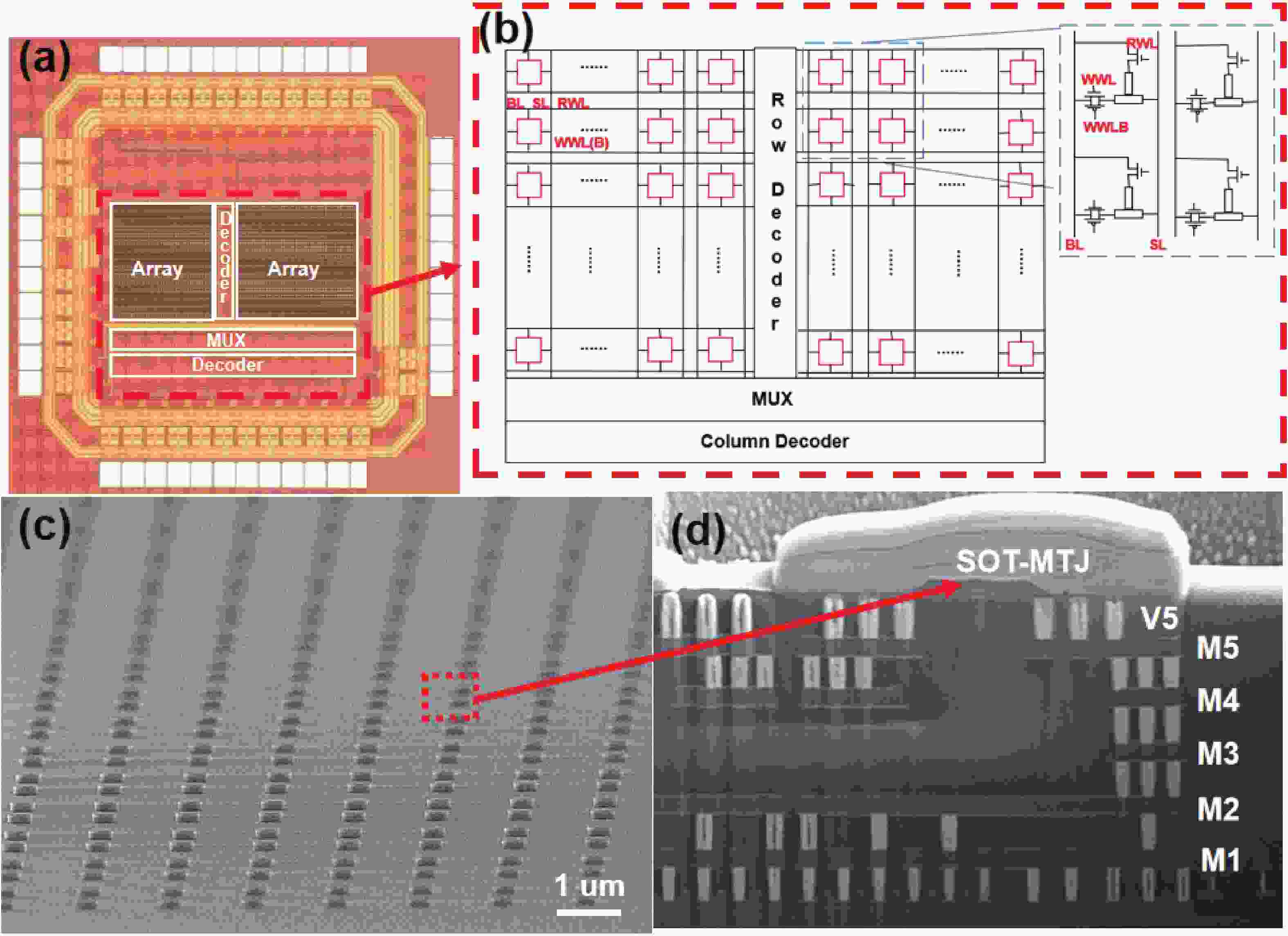
Fig. 1.  (Color online) (a) A top view of 1 Kb SOT MRAM MUX array observed by an optical microscope. The size of the MUX array is about 1 × 1 mm2. (b) The 1 Kb SOT-MRAM MUX array includes a row address decoder, a column address decoder, SOT arrays, and a MUX circuit. (c) A zoom-in SEM image of the MUX array after the MTJ etch process. Each pillar in the SEM image represents an elliptical shape MTJ with CD of 300, 1050 nm for short axis a and long axis b, respectively. (d) The cross-section TEM of a selected MTJ in the array from the fully processed wafer in conjunction with CMOS using common 0.18 μm CMOS process technology node. The SOT-MTJ is integrated between the “Metal 5” and the passivation layer.

Fig. 2.  (Color online) (a) The quantile plot of the RP and RAP distributions of the 1 Kb SOT-MRAM MUX array. The RP and RAP were measured after the SOT-MTJs were set to either the P or AP states under appropriate write bias voltages. The RP and RAP were normalized to the average value of the RP in the 1 Kb MUX array. The arrows indicate the separation gap between the RP and RAP statistically. (b) The correlation between the TMR and the RP. Each dot in the figure indicates one SOT-MTJ. The resistance in horizontal axis of (b) is normalized by the average value of the RP.

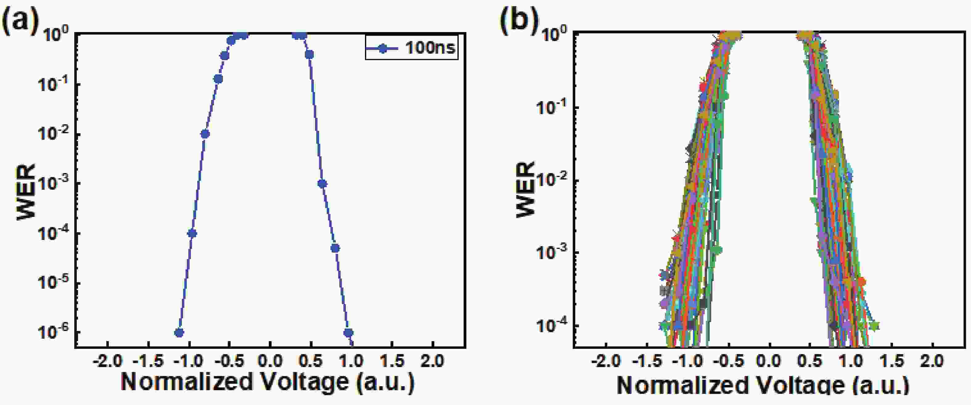
Fig. 3.  (Color online) (a) Typical WER curves down to 10−6 level measured under 100 ns write pulse widths; (b) WER curves down to 10−4 level were collected from over 70 SOT-MTJs under 100 ns write pulse widths. The positive and negative bias voltages in (a) and (b) correspond to the write AP and P directions respectively. Each point in (a) and (b) represents the write failure rate for devices tested over 1 million cycles under each constant bias voltage.

Fig. 4.  (Color online) The temperature dependence of (a) the TMR ratios and (b) switching critical switching densities. (c) The CDF plot of the critical current densities from the data in (b). Blue, red and green box plots/dots represent the values at –40, 25, and 125 °C, respectively. The current densities in (b) and (c) are normalized to the median value of 19 MA/cm2 at 25 °C.

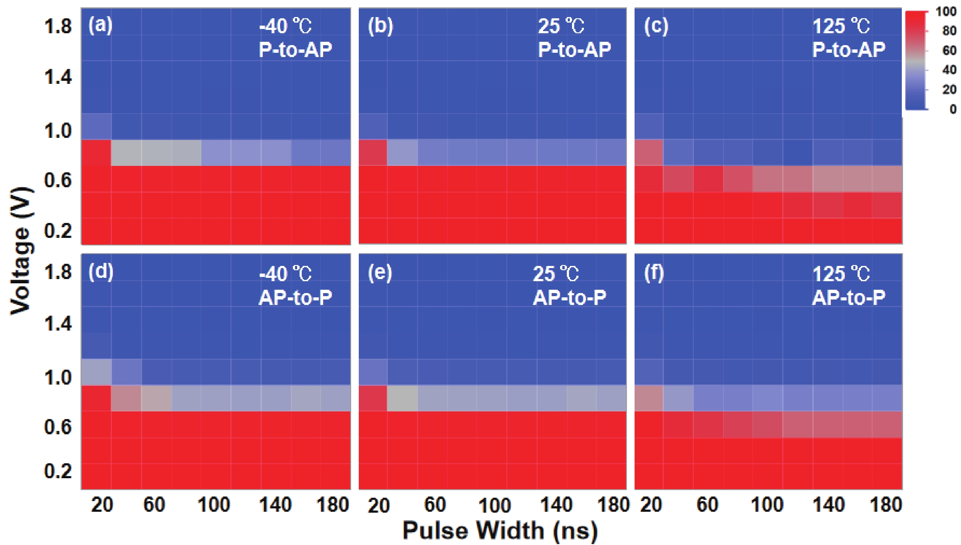
Fig. 5.  (Color online) Write shmoo plots of the 1 Kb MUX array at different temperatures from −40, 25, and 125 °C, respectively. (a)−(c) are for the P-to-AP direction, and (d)−(f) are for the AP-to-P direction. The shmoo plots show the write failure rates of 1 Kb in the MUX array at each write speed (x-axis) and each write bias voltage (y-axis). The pulse widths vary from 20 to 200 ns and the bias voltages range from 0.2 to 1.8 V, respectively. The write failure rates are presented in color gradient with the scale bar shown on the right: red represents 100% fail and blue represents zero fail.

Table 1.   Performance comparison of SOT-MRAM.

Items This work Ref. [34] Ref. [35] Ref. [38] Ref. [39] Ref. [40] Ref. [41] Ref. [42]
SOT channel
Device type
β-W
IMA
W
PMA
β-W
IMA
W
IMA
W
IMA
Pt
PMA
Pt
IMA
β-W
PMA
MTJ CD (nm) 300 × 1050 60 88 × 315 240 × 840 75 × 230 50 700 60
TMR (%) >80 110 167 85 140 90/125 101 105
WER <10−6 10−5 N/A N/A 10−4 N/A N/A N/A
Jc (MA/cm2) 28 @20 ns 126 @1 ns 23.6 @0.35 ns 81 61 @1 ns 110 @1 ns 170 @10 ns 57 @1 ns
Function yield 99.6% N/A N/A N/A 98% N/A N/A N/A
DownLoad: CSV
[1]
Clarke P. TSMC embedded MRAM is key to Gyrfalcon AI chip. Technology News, 2018, [2018-9-22]. https://www.eenewseurope.com/
[2]
Choe J. TSMC 22ULL eMRAM Die removed from Ambiq Apollo-4, Another Disruptive Technology on Embedded Memory. TechInsights TechStream Blog_Emerging Memory, 2021 [2021-8-13]. https://www.techinsights.com/
[3]
Choe J. Recent technology insights on STT-MRAM: Structure, materials, and process integration. 2023 IEEE International Memory Workshop (IMW), Monterey, 2023, 1 doi: 10.1109/IMW56887.2023.10145822
[4]
Chiang H L, Wang J F, Chen T C, et al. Cold MRAM as a density booster for embedded NVM in advanced technology. 2021 Symposium on VLSI Technology, 2021, 1
[5]
Chen C H, Chang C Y, Weng C H, et al. Reliability and magnetic immunity of reflow-capable embedded STT-MRAM in 16nm FinFET CMOS process. 2021 Symposium on VLSI Technology, 2021, 1
[6]
Wang C Y, Shih M C, Weng C H, et al. Reliability demonstration of reflow qualified 22nm STT-MRAM for embedded memory applications. 2020 IEEE Symposium on VLSI Technology, 2020, 1 doi: 10.1109/VLSITechnology18217.2020.9265054
[7]
Lee K, Yamane K, Noh S, et al. 22-nm FD-SOI embedded MRAM with full solder reflow compatibility and enhanced magnetic immunity. 2018 IEEE Symposium on VLSI Technology, 2018, 183 doi: 10.1109/VLSIT.2018.8510655
[8]
Naik V B, Lee K, Yamane K, et al. Manufacturable 22nm FD-SOI embedded MRAM technology for industrial-grade MCU and IOT applications. 2019 IEEE International Electron Devices Meeting (IEDM), 2019, 2.3.1 doi: 10.1109/IEDM19573.2019.8993454
[9]
Naik V B, Yamane K, Kwon J, et al. STT-MRAM: A robust embedded non-volatile memory with superior reliability and immunity to external magnetic field and RF sources. Proceedings of 2021 IEEE Symposium on VLSI Technology, 2021, 1
[10]
Naik V B, Yamane K, Lee T Y, et al. JEDEC-qualified highly reliable 22nm FD-SOI embedded MRAM for low-power industrial-grade, and extended performance towards automotive-grade-1 applications. 2020 IEEE International Electron Devices Meeting (IEDM), 2021, 11.3.1 doi: 10.1109/IEDM13553.2020.9371935
[11]
Lee K, Bak J H, Kim Y J, et al. 1Gbit high density embedded STT-MRAM in 28nm FDSOI technology. 2019 IEEE International Electron Devices Meeting (IEDM), 2019, 2.2.1 doi: 10.1109/IEDM19573.2019.8993551
[12]
Lee K, Kim D S, Bak J H, et al. 28nm CIS-compatible embedded STT-MRAM for frame buffer memory. 2021 IEEE International Electron Devices Meeting (IEDM), 2021, 2.1.1 doi: 10.1109/IEDM19574.2021.9720537
[13]
Suh K, Lee J H, Shin H M, et al. 12.5 Mb/mm2 embedded MRAM for high density non-volatile RAM applications. 2021 Symposium on VLSI Technology, 2021, 1
[14]
Endoh T, Honjo H, Nishioka K, et al. Recent progresses in STT-MRAM and SOT-MRAM for next generation MRAM. 2020 IEEE Symposium on VLSI Technology, 2020, 1 doi: 10.1109/VLSITechnology18217.2020.9265042
[15]
Rao S, Kim W, van Beek S, et al. STT-MRAM array performance improvement through optimization of Ion beam etch and MTJ for last-level cache application. 2021 IEEE International Memory Workshop (IMW), 2021, 1 doi: 10.1109/IMW51353.2021.9439592
[16]
Wu H, Katragadda V, Evarts E, et al. First experimental demonstration of MRAM data scrubbing: 80 Mb MRAM with 40 nm junctions for last level cache applications. 2021 IEEE International Electron Devices Meeting (IEDM), 2021, 2.3.1 doi: 10.1109/IEDM19574.2021.9720539
[17]
Edelstein D, Rizzolo M, Sil D, et al. A 14 nm embedded STT-MRAM CMOS technology. 2020 IEEE International Electron Devices Meeting (IEDM), 2020, 11.5.1 doi: 10.1109/IEDM13553.2020.9371922
[18]
Worledge D C. Spin-transfer-torque MRAM: The next revolution in memory. 2022 IEEE International Memory Workshop (IMW), 2022, 1 doi: 10.1109/IMW52921.2022.9779288
[19]
Mihai Miron I, Gaudin G, Auffret S, et al. Current-driven spin torque induced by the Rashba effect in a ferromagnetic metal layer. Nat Mater, 2010, 9, 230 doi: 10.1038/nmat2613
[20]
Miron I M, Garello K, Gaudin G, et al. Perpendicular switching of a single ferromagnetic layer induced by in-plane current injection. Nature, 2011, 476, 189 doi: 10.1038/nature10309
[21]
Cubukcu M, Boulle O, Drouard M, et al. Spin-orbit torque magnetization switching of a three-terminal perpendicular magnetic tunnel junction. Appl Phys Lett, 2014, 104, 042406 doi: 10.1063/1.4863407
[22]
Liu L Q, Lee O J, Gudmundsen T J, et al. Current-induced switching of perpendicularly magnetized magnetic layers using spin torque from the spin Hall effect. Phys Rev Lett, 2012, 109, 096602 doi: 10.1103/PhysRevLett.109.096602
[23]
Liu L Q, Pai C F, Li Y, et al. Spin-torque switching with the giant spin Hall effect of tantalum. Science, 2012, 336, 555 doi: 10.1126/science.1218197
[24]
Pai C F, Liu L Q, Li Y, et al. Spin transfer torque devices utilizing the giant spin Hall effect of tungsten. Appl Phys Lett, 2012, 101, 122404 doi: 10.1063/1.4753947
[25]
Shao Q M, Li P, Liu L Q, et al. Roadmap of spin–orbit torques. IEEE Trans Magn, 2021, 57, 1 doi: 10.1109/TMAG.2021.3078583
[26]
Guo Z X, Yin J L, Bai Y, et al. Spintronics for energy- efficient computing: An overview and outlook. Proc IEEE, 2021, 109, 1398 doi: 10.1109/JPROC.2021.3084997
[27]
Van Beek S, Cai K M, Fan K Q, et al. MTJ degradation in multi-pillar SOT-MRAM with selective writing. 2023 IEEE International Reliability Physics Symposium (IRPS), 2023, 1 doi: MTJdegradationinmulti-pil-larSOT-MRAMwithselectivewriting
[28]
Xu X Y, Zhang H C, Jiang C P, et al. Full reliability characterization of three-terminal SOT-MTJ devices and corresponding arrays. 2023 IEEE International Reliability Physics Symposium (IRPS), 2023, 1 doi: 10.1109/IRPS48203.2023.10117643
[29]
Sverdlov V, Makarov A, Selberherr S. Two-pulse sub-ns switching scheme for advanced spin-orbit torque MRAM. Solid State Electron, 2019, 155, 49 doi: 10.1016/j.sse.2019.03.010
[30]
Lee K S, Lee S W, Min B C, et al. Threshold current for switching of a perpendicular magnetic layer induced by spin Hall effect. Appl Phys Lett, 2013, 102, 112410 doi: 10.1063/1.4798288
[31]
Liu H, Bedau D, Sun J Z, et al. Dynamics of spin torque switching in all-perpendicular spin valve nanopillars. J Magn Magn Mater, 2014, 358, 233 doi: 10.1016/j.jmmm.2014.01.061
[32]
Wang M X, Cai W L, Zhu D Q, et al. Field-free switching of a perpendicular magnetic tunnel junction through the interplay of spin-orbit and spin-transfer torques. Nat Electron, 2018, 1, 582 doi: 10.1038/s41928-018-0160-7
[33]
Garello K, Yasin F, Couet S, et al. SOT-MRAM 300MM integration for low power and ultrafast embedded memories. 2018 IEEE Symposium on VLSI Circuits, 2018, 81 doi: 10.1109/VLSIC.2018.8502269
[34]
Garello K, Yasin F, Hody H, et al. Manufacturable 300mm platform solution for field-free switching SOT-MRAM. 2019 Symposium on VLSI Circuits, 2019, T194 doi: 10.23919/VLSIC.2019.8778100
[35]
Honjo H, Nguyen T V A, Watanabe T, et al. First demonstration of field-free SOT-MRAM with 0.35 ns write speed and 70 thermal stability under 400°C thermal tolerance by canted SOT structure and its advanced patterning/SOT channel technology. 2019 IEEE International Electron Devices Meeting (IEDM), 2020, 28.5.1 doi: 10.1109/IEDM19573.2019.8993443
[36]
Wu Y C, Kim W, Garello K, et al. Deterministic and field-free voltage-controlled MRAM for high performance and low power applications. 2020 IEEE Symposium on VLSI Technology, 2020, 1 doi: 10.1109/VLSITechnology18217.2020.9265057
[37]
Natsui M, Tamakoshi A, Honjo H, et al. Dual-port SOT-MRAM achieving 90-MHz read and 60-MHz write operations under field-assistance-free condition. IEEE J Solid-State Circuits, 2021, 56, 1116 doi: 10.1109/JSSC.2020.3039800
[38]
Chen G L, Wang I J, Yeh P S, et al. An 8kb spin-orbit-torque magnetic random-access memory. 2021 International Symposium on VLSI Technology, Systems and Applications (VLSI-TSA), 2021, 1 doi: 10.1109/VLSI-TSA51926.2021.9440096
[39]
Song M Y, Lee C M, Yang S Y, et al. High speed (1ns) and low voltage (1.5V) demonstration of 8Kb SOT-MRAM array. 2022 IEEE Symposium on VLSI Technology and Circuits (VLSI Technology and Circuits), 2022, 377 doi: 10.1109/VLSITechnologyandCir46769.2022.9830149
[40]
Couet S, Rao S, Van Beek S, et al. BEOL compatible high retention perpendicular SOT-MRAM device for SRAM replacement and machine learning. 2021 Symposium on VLSI Technology, 2021, 1
[41]
Zhu D Q, Guo Z X, Du A, et al. First demonstration of three terminal MRAM devices with immunity to magnetic fields and 10 ns field free switching by electrical manipulation of exchange bias. 2021 IEEE International Electron Devices Meeting (IEDM), 2022, 17.5.1 doi: 10.1109/IEDM19574.2021.9720599
[42]
Cai K, Talmelli G, Fan K, et al. First demonstration of field-free perpendicular SOT-MRAM for ultrafast and high-density embedded memories. 2022 International Electron Devices Meeting (IEDM), 2023, 36.2.1 doi: 10.1109/IEDM45625.2022.10019360
[43]
Rahaman S Z, Chang Y J, Hsin Y C, et al. Development of highly manufacturable, reliable, and energy-efficient spin-orbit torque magnetic random access memory (SOT-MRAM). 2022 International Symposium on VLSI Technology, Systems and Applications (VLSI-TSA), 2022, 1 doi: 10.1109/VLSI-TSA54299.2022.9771005
[44]
Krizakova V, Perumkunnil M, Couet S, et al. Spin-orbit torque switching of magnetic tunnel junctions for memory applications. J Magn Magn Mater, 2022, 562, 169692 doi: 10.1016/j.jmmm.2022.169692
[45]
Lin S J, Huang Y L, Song M, et al. Challenges toward low-power SOT-MRAM. 2021 IEEE International Reliability Physics Symposium (IRPS), 2021, 1 doi: 10.1109/IRPS46558.2021.9405127
[46]
Zhang H C, Ma X Y, Jiang C P, et al. Integration of high-performance spin-orbit torque MRAM devices by 200-mm-wafer manufacturing platform. J Semicond, 2022, 43, 102501 doi: 10.1088/1674-4926/43/10/102501
[47]
Park J H, Lee J, Jeong J, et al. A novel integration of STT-MRAM for on-chip hybrid memory by utilizing non-volatility modulation. 2019 IEEE International Electron Devices Meeting (IEDM), 2020, 2.5.1 doi: 10.1109/IEDM19573.2019.8993614
[48]
Fukami S, Anekawa T, Zhang C, et al. A spin-orbit torque switching scheme with collinear magnetic easy axis and current configuration. Nat Nanotechnol, 2016, 11, 621 doi: 10.1038/nnano.2016.29
[49]
Lee K, Chao R, Yamane K, et al. 22-nm FD-SOI embedded MRAM technology for low-power automotive-grade-l MCU applications. 2018 IEEE International Electron Devices Meeting (IEDM), 2019, 27.1.1 doi: 10.1109/IEDM.2018.8614566
[50]
Min T, Chen Q, Beach R, et al. A study of write margin of spin torque transfer magnetic random access memory technology. IEEE Trans Magn, 2010, 46, 2322 doi: 10.1109/TMAG.2010.2043069
[51]
Kim W, Couet S, Swerts J, et al. Experimental observation of back-hopping with reference layer flipping by high-voltage pulse in perpendicular magnetic tunnel junctions. IEEE Trans Magn, 2016, 52, 1 doi: 10.1109/TMAG.2016.2536158
[52]
Tan J, Lim J H, Sikder B, et al. Impact of voltage polarity on time-dependent dielectric breakdown of 1-nm MgO-based STT-MRAM with self-heating correction. IEEE Trans Electron Devices, 2022, 70, 76 doi: 10.1109/TED.2022.3220485
[53]
Zhao W S, Chappert C, Javerliac V, et al. High speed, high stability and low power sensing amplifier for MTJ/CMOS hybrid logic circuits. IEEE Trans Magn, 2009, 45, 3784 doi: 10.1109/TMAG.2009.2024325
[54]
Song Y J, Lee J H, Shin H C, et al. Highly functional and reliable 8Mb STT-MRAM embedded in 28nm logic. 2016 IEEE International Electron Devices Meeting (IEDM), 2017, 27.2.1 doi: 10.1109/IEDM.2016.7838491
  • Search

    Advanced Search >>

    GET CITATION

    shu

    Export: BibTex EndNote

    Article Metrics

    Article views: 918 Times PDF downloads: 178 Times Cited by: 0 Times

    History

    Received: 07 September 2023 Revised: 21 September 2023 Online: Accepted Manuscript: 31 October 2023Corrected proof: 02 November 2023Uncorrected proof: 03 November 2023Published: 10 December 2023

    Catalog

      Email This Article

      User name:
      Email:*请输入正确邮箱
      Code:*验证码错误
      Chuanpeng Jiang, Jinhao Li, Hongchao Zhang, Shiyang Lu, Pengbin Li, Chao Wang, Zhongkui Zhang, Zhengyi Hou, Xu Liu, Jiagao Feng, He Zhang, Hui Jin, Gefei Wang, Hongxi Liu, Kaihua Cao, Zhaohao Wang, Weisheng Zhao. Demonstration of a manufacturable SOT-MRAM multiplexer array towards industrial applications[J]. Journal of Semiconductors, 2023, 44(12): 122501. doi: 10.1088/1674-4926/44/12/122501 C P Jiang, J H Li, H C Zhang, S Y Lu, P B Li, C Wang, Z K Zhang, Z Y Hou, X Liu, J G Feng, H Zhang, H Jin, G F Wang, H X Liu, K H Cao, Z H Wang, W S Zhao. Demonstration of a manufacturable SOT-MRAM multiplexer array towards industrial applications[J]. J. Semicond, 2023, 44(12): 122501. doi: 10.1088/1674-4926/44/12/122501Export: BibTex EndNote
      Citation:
      Chuanpeng Jiang, Jinhao Li, Hongchao Zhang, Shiyang Lu, Pengbin Li, Chao Wang, Zhongkui Zhang, Zhengyi Hou, Xu Liu, Jiagao Feng, He Zhang, Hui Jin, Gefei Wang, Hongxi Liu, Kaihua Cao, Zhaohao Wang, Weisheng Zhao. Demonstration of a manufacturable SOT-MRAM multiplexer array towards industrial applications[J]. Journal of Semiconductors, 2023, 44(12): 122501. doi: 10.1088/1674-4926/44/12/122501

      C P Jiang, J H Li, H C Zhang, S Y Lu, P B Li, C Wang, Z K Zhang, Z Y Hou, X Liu, J G Feng, H Zhang, H Jin, G F Wang, H X Liu, K H Cao, Z H Wang, W S Zhao. Demonstration of a manufacturable SOT-MRAM multiplexer array towards industrial applications[J]. J. Semicond, 2023, 44(12): 122501. doi: 10.1088/1674-4926/44/12/122501
      Export: BibTex EndNote

      Demonstration of a manufacturable SOT-MRAM multiplexer array towards industrial applications

      doi: 10.1088/1674-4926/44/12/122501
      More Information
      • Author Bio:

        Chuanpeng Jiang Chuanpeng Jiang (M’97) received the B.S. degree in college of electronics and information from Qingdao University, Shandong, China, in 2020. He is currently working toward a Ph.D. degree in integrated circuit science and engineering at Beihang University, Beijing, China. His current research interests include fabrication processes for magnetic tunnel junctions and characterization of SOT-MRAM device properties

        Hongxi Liu Hongxi Liu received the Ph.D. degree in Electronics for Informatics from Hokkaido University, Japan, in 2012. He has worked in academia and industry for over 10 years, mainly focusing on the research and development of MRAM technology. He is currently in charge of the activities of SOT MRAM R&D in Truth Memory tech. Corporation, Beijing, China

        Kaihua Cao Zhaohao Wang (M’87) received the B.S. degree in microelectronics from Tianjin University, China, in 2009, the M.S. degree in microelectronics from Beihang University, China, in 2012, and the Ph.D. degree in physics from University Paris-Saclay, France, in 2015. He is currently an associate professor at School of Integrated Circuit Science and Engineering, Beihang University, China. His current research interests include the modeling of non-volatile nano-devices and the design of emerging non-volatile memories and logic circuits

      • Corresponding author: hongxi_liu@tmc-bj.cnkaihua_cao@tmc-bj.cnzhaohao.wang@buaa.edu.cn
      • Received Date: 2023-09-07
      • Revised Date: 2023-09-21
      • Available Online: 2023-10-31

      Catalog

        /

        DownLoad:  Full-Size Img  PowerPoint
        Return
        Return