| [1] |
Lopez-Sanchez O, Lembke D, Kayci M, et al. Ultrasensitive photodetectors based on monolayer MoS 2. Nat Nanotechnol, 2013, 8, 497 doi: 10.1038/nnano.2013.100 |
| [2] |
Zhang W J, Huang J K, Chen C H, et al. High-gain phototransistors based on a CVD MoS 2 monolayer. Adv Mater, 2013, 25, 3456 doi: 10.1002/adma.201301244 |
| [3] |
Chang Y H, Zhang W J, Zhu Y H, et al. Monolayer MoSe 2 grown by chemical vapor deposition for fast photodetection. ACS Nano, 2014, 8, 8582 doi: 10.1021/nn503287m |
| [4] |
Anichini C, Czepa W, Pakulski D, et al. Chemical sensing with 2D materials. Chem Soc Rev, 2018, 47, 4860 doi: 10.1039/C8CS00417J |
| [5] |
Xu S P, Fu H X, Tian Y, et al. Exploiting two-dimensional Bi 2O 2Se for trace oxygen detection. Angew Chem Int Ed, 2020, 59, 17938 doi: 10.1002/anie.202006745 |
| [6] |
Shehzad K, Shi T J, Qadir A, et al. Environmental sensing: Designing an efficient multimode environmental sensor based on graphene-silicon heterojunction. Adv Mater Technol, 2017, 2, 1600262 doi: 10.1002/admt.201600262 |
| [7] |
Li J F, Liang Z Z, Wang Y F, et al. Enhanced efficiency of polymer solar cells through synergistic optimization of mobility and tuning donor alloys by adding high-mobility conjugated polymers. J Mater Chem C, 2018, 6, 11015 doi: 10.1039/C8TC03612H |
| [8] |
Vu Q A, Kim H, Nguyen V L, et al. Memristors: A high-on/off-ratio floating-gate memristor array on a flexible substrate via CVD-grown large-area 2D layer stacking. Adv Mater, 2017, 29, 1703363 doi: 10.1002/adma.201703363 |
| [9] |
Novoselov K S, Geim A K, Morozov S V, et al. Electric field effect in atomically thin carbon films. Science, 2004, 306, 666 doi: 10.1126/science.1102896 |
| [10] |
Brown A, Rundqvist S. Refinement of the crystal structure of black phosphorus. Acta Cryst, 1965, 19, 684 doi: 10.1107/S0365110X65004140 |
| [11] |
Wu J X, Yuan H T, Meng M M, et al. High electron mobility and quantum oscillations in non-encapsulated ultrathin semiconducting Bi 2O 2Se. Nat Nanotechnol, 2017, 12, 530 doi: 10.1038/nnano.2017.43 |
| [12] |
Zhao Y T, Wang H Y, Huang H, et al. Back cover: Surface coordination of black phosphorus for robust air and water stability (Angew. Chem. Int. Ed. 16/2016). Angew Chem Int Ed, 2016, 55, 5097 doi: 10.1002/anie.201602471 |
| [13] |
Mak K F, Lee C, Hone J, et al. Atomically thin MoS 2: A new direct-gap semiconductor. Phys Rev Lett, 2010, 105, 136805 doi: 10.1103/PhysRevLett.105.136805 |
| [14] |
Li L K, Yu Y J, Ye G J, et al. Black phosphorus field-effect transistors. Nat Nanotechnol, 2014, 9, 372 doi: 10.1038/nnano.2014.35 |
| [15] |
Radisavljevic B, Radenovic A, Brivio J, et al. Single-layer MoS 2 transistors. Nat Nanotechnol, 2011, 6, 147 doi: 10.1038/nnano.2010.279 |
| [16] |
Wei Q, Li R, Lin C, et al. Quasi-two-dimensional se-terminated bismuth oxychalcogenide (Bi 2O 2Se). ACS Nano, 2019, 13, 13439 doi: 10.1021/acsnano.9b07000 |
| [17] |
|
| [18] |
Zhang C, Wu J, Sun Y, et al. High-mobility flexible oxyselenide thin-film transistors prepared by a solution-assisted method. J Am Chem Soc, 2020, 142, 2726 doi: 10.1021/jacs.9b11668 |
| [19] |
Tan C, Tang M, Wu J, et al. Wafer-Scale growth of single-crystal 2D semiconductor on perovskite oxides for high-performance transistors. Nano Lett, 2019, 19, 2148 doi: 10.1021/acs.nanolett.9b00381 |
| [20] |
Khan U, Luo Y, Tang L, et al. Controlled vapor–solid deposition of millimeter-size single crystal 2D Bi 2O 2Se for high-performance phototransistors. Adv Funct Mater, 2019, 29, 1807979 doi: 10.1002/adfm.201807979 |
| [21] |
Chen G, Wu J, Wang B, et al. High-performance self-powered photodetector based on Bi 2O 2Se nanosheets. Appl Phys A, 2020, 126, 579 doi: 10.1007/s00339-020-03759-0 |
| [22] |
Xu R, Wang S, Li Y, et al. Layered semiconductor Bi 2O 2Se for broadband pulse generation in the near-infrared. IEEE Photonics Technol Lett, 2019, 31, 1056 doi: 10.1109/LPT.2019.2917472 |
| [23] |
Xie H H, Liu M Q, You B H, et al. Photothermal therapy: Biodegradable Bi 2O 2Se quantum dots for photoacoustic imaging-guided cancer photothermal therapy. Small, 2020, 16, 2070013 doi: 10.1002/smll.202070013 |
| [24] |
Yang C, Chen T, Verma D, et al. Bidirectional all-optical synapses based on a 2D Bi 2O 2Se/graphene hybrid structure for multifunctional optoelectronics. Adv Funct Mater, 2020, 30, 2001598 doi: 10.1002/adfm.202001598 |
| [25] |
Zhang Z Y, Li T R, Wu Y J, et al. Truly concomitant and independently expressed short-and long-term plasticity in a Bi 2O 2Se-based three-terminal memristor. Adv Mater, 2019, 31, 1805769 doi: 10.1002/adma.201805769 |
| [26] |
Allen M J, Tung V C, Kaner R B. Honeycomb carbon: A review of graphene. Chem Rev, 2010, 110, 132 doi: 10.1021/cr900070d |
| [27] |
Huang X, Zeng Z Y, Zhang H. Metal dichalcogenide nanosheets: Preparation, properties and applications. Chem Soc Rev, 2013, 42, 1934 doi: 10.1039/c2cs35387c |
| [28] |
Nicolosi V, Chhowalla M, Kanatzidis M G, et al. Liquid exfoliation of layered materials. Science, 2013, 340, 1226419 doi: 10.1126/science.1226419 |
| [29] |
Huang Y, Pan Y H, Yang R, et al. Universal mechanical exfoliation of large-area 2D crystals. Nat Commun, 2020, 11, 2453 doi: 10.1038/s41467-020-16266-w |
| [30] |
Fu Q, Dai J Q, Huang X Y, et al. One-step exfoliation method for plasmonic activation of large-area 2D crystals. Adv Sci, 2022, 2204247
|
| [31] |
Wu J X, Tan C W, Tan Z J, et al. Controlled synthesis of high-mobility atomically thin bismuth oxyselenide crystals. Nano Lett, 2017, 17, 3021 doi: 10.1021/acs.nanolett.7b00335 |
| [32] |
Wu J X, Qiu C G, Fu H X, et al. Low residual carrier concentration and high mobility in 2D semiconducting Bi 2O 2Se. Nano Lett, 2019, 19, 197 doi: 10.1021/acs.nanolett.8b03696 |
| [33] |
Tong T, Chen Y F, Qin S C, et al. Sensitive and ultrabroadband phototransistor based on two-dimensional Bi 2O 2Se nanosheets. Adv Funct Mater, 2019, 29, 1905806 doi: 10.1002/adfm.201905806 |
| [34] |
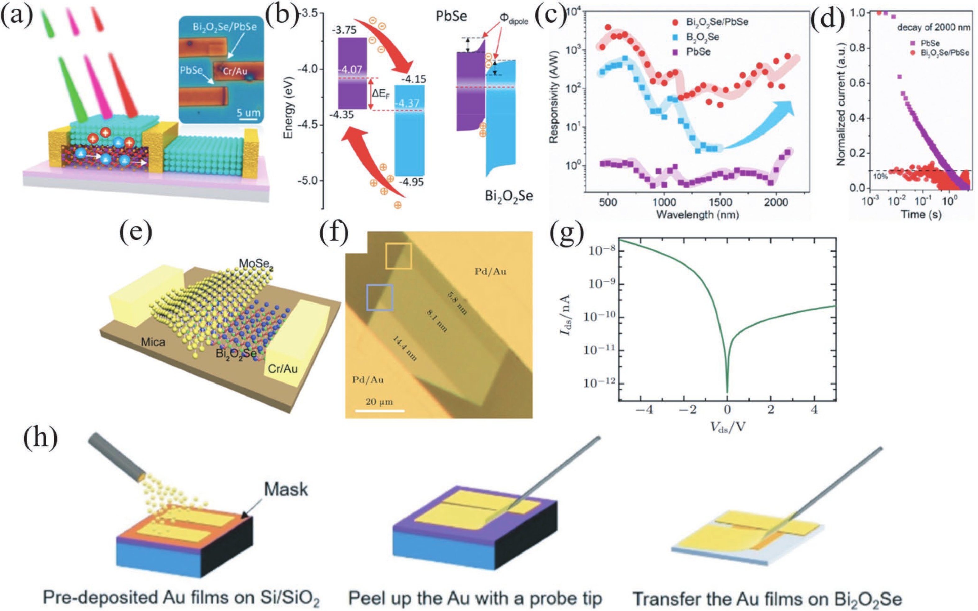
Fu Q D, Zhu C, Zhao X X, et al. Ultrasensitive 2D Bi 2O 2Se phototransistors on silicon substrates. Adv Mater, 2019, 31, 1804945 doi: 10.1002/adma.201804945 |
| [35] |
Khan U, Tang L, Ding B F, et al. Nanoribbons: Catalyst-free growth of atomically thin Bi 2O 2Se nanoribbons for high-performance electronics and optoelectronics. Adv Funct Mater, 2021, 31, 2170230 doi: 10.1002/adfm.202170230 |
| [36] |
Avishan N, Hussain N, Nosheen F. Large-scale graphene production and transfer for industrial applications. MaterInnov, 2022, 2, 15
|
| [37] |
Chen C, Wang M X, Wu J X, et al. Electronic structures and unusually robust bandgap in an ultrahigh-mobility layered oxide semiconductor, Bi 2O 2Se. Sci Adv, 2018, 4, eaat8355 doi: 10.1126/sciadv.aat8355 |
| [38] |
Zeng T, You Y C, Wang X F, et al. Chemical vapor deposition and device application of two-dimensional molybdenum disulfide-based atomic crystals. Prog Chem, 2016, 28, 459 doi: 10.7536/PC151026 |
| [39] |
Yu J X, Li J, Zhang W F, et al. Synthesis of high quality two-dimensional materials via chemical vapor deposition. Chem Sci, 2015, 6, 6705 doi: 10.1039/C5SC01941A |
| [40] |
Yin J B, Tan Z J, Hong H, et al. Ultrafast and highly sensitive infrared photodetectors based on two-dimensional oxyselenide crystals. Nat Commun, 2018, 9, 3311 doi: 10.1038/s41467-018-05874-2 |
| [41] |
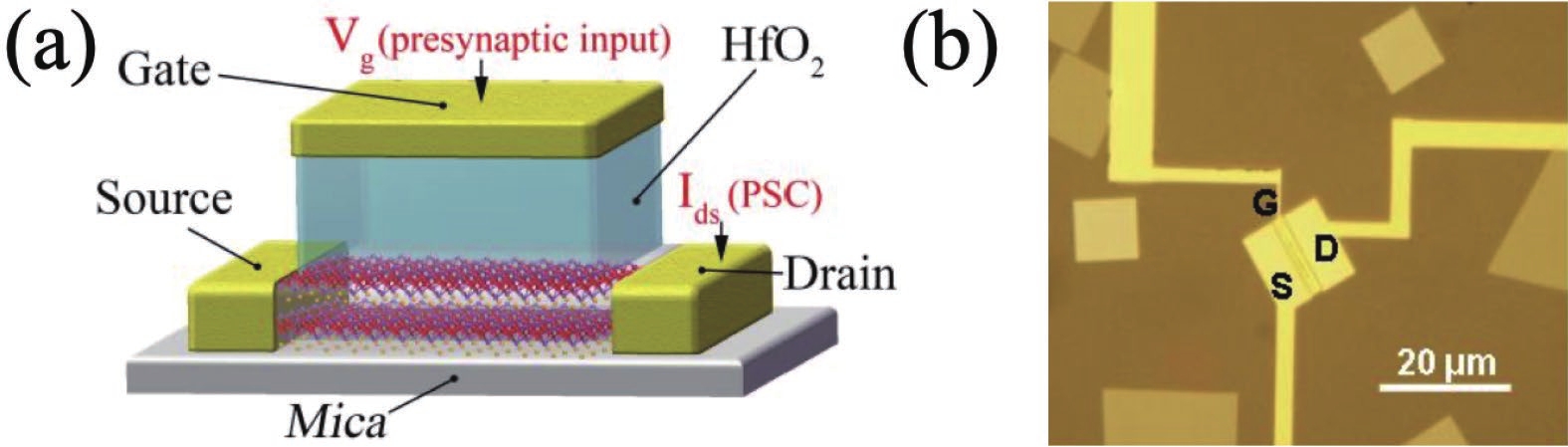
Li J, Wang Z X, Wen Y, et al. High-performance near-infrared photodetector based on ultrathin Bi 2O 2Se nanosheets. Adv Funct Mater, 2018, 28, 1706437 doi: 10.1002/adfm.201706437 |
| [42] |
Fu H X, Wu J X, Peng H L, et al. Self-modulation doping effect in the high-mobility layered semiconductor Bi 2O 2Se. Phys Rev B, 2018, 97, 241203 doi: 10.1103/PhysRevB.97.241203 |
| [43] |
Wu Z, Liu G L, Wang Y X, et al. Seed-induced vertical growth of 2D Bi 2O 2Se nanoplates by chemical vapor transport. Adv Funct Mater, 2019, 29, 1906639 doi: 10.1002/adfm.201906639 |
| [44] |
Chen W J, Khan U, Feng S M, et al. High-fidelity transfer of 2D Bi 2O 2Se and its mechanical properties. Adv Funct Mater, 2020, 30, 2004960 doi: 10.1002/adfm.202004960 |
| [45] |
Zhang X, Liu Y F, Zhang G H, et al. Thermal decomposition of bismuth oxysulfide from photoelectric Bi 2O 2S to superconducting Bi 4O 4S 3. ACS Appl Mater Interfaces, 2015, 7, 4442 doi: 10.1021/am5092159 |
| [46] |
Tian X L, Luo H Y, Wei R F, et al. Pulsed lasers: An ultrabroadband mid-infrared pulsed optical switch employing solution-processed bismuth oxyselenide. Adv Mater, 2018, 30, 1870233 doi: 10.1002/adma.201870233 |
| [47] |
Yang X, Zhang Q, Song Y C, et al. High mobility two-dimensional bismuth oxyselenide single crystals with large grain size grown by reverse-flow chemical vapor deposition. ACS Appl Mater Interfaces, 2021, 13, 49153 doi: 10.1021/acsami.1c13491 |
| [48] |
Li M Q, Dang l L Y, Wang G G, et al. Bismuth oxychalcogenide nanosheet: Facile synthesis, characterization, and photodetector application. Adv Mater Technol, 2020, 5, 2000180 doi: 10.1002/admt.202000180 |
| [49] |
Dang L Y, Liu M Q, Wang G G, et al. Organic ion template-guided solution growth of ultrathin bismuth oxyselenide with tunable electronic properties for optoelectronic applications. Adv Funct Mater, 2022, 32, 2201020 doi: 10.1002/adfm.202201020 |
| [50] |
Tong T, Zhang M H, Chen Y Q, et al. Ultrahigh Hall mobility and suppressed backward scattering in layered semiconductor Bi 2O 2Se. Appl Phys Lett, 2018, 113, 072106 doi: 10.1063/1.5042727 |
| [51] |
Williams M L. CRC handbook of chemistry and physics. 76th ed. Occup Environ Med, 1996, 53, 504 doi: 10.1136/oem.53.7.504 |
| [52] |
Horák J, Stary Z, Lošťák P, et al. Anti-site defects in n-Bi 2Se 3 crystals. J Phys Chem Solids, 1990, 51, 1353 doi: 10.1016/0022-3697(90)90017-A |
| [53] |
Pereira A L J, Santamaría-Pérez D, Vilaplana R, et al. Experimental and theoretical study of SbPO 4 under compression. Inorg Chem, 2020, 59, 287 doi: 10.1021/acs.inorgchem.9b02268 |
| [54] |
Pan X, Chen H X, Lu L, et al. Incorporating guanidinium as perovskitizer-cation of two-dimensional metal halide for crystal-array photodetectors. Chem Asian J, 2021, 16, 1925 doi: 10.1002/asia.202100425 |
| [55] |
Cheng T, Tan C W, Zhang S Q, et al. Raman spectra and strain effects in bismuth oxychalcogenides. J Phys Chem C, 2018, 122, 19970 doi: 10.1021/acs.jpcc.8b05475 |
| [56] |
Liu S Y, Tan C W, He D W, et al. Optical properties and photocarrier dynamics of Bi 2O 2Se monolayer and nanoplates. Adv Optical Mater, 2020, 8, 1901567 doi: 10.1002/adom.201901567 |
| [57] |
Zhang Y, Gao Q, Han X Y, et al. Mechanical flexibility and strain engineered-band structures of monolayer Bi 2O 2Se. Phys E, 2020, 116, 113728 doi: 10.1016/j.physe.2019.113728 |
| [58] |
Guo D L, Hu C G, Xi Y, et al. Strain effects to optimize thermoelectric properties of doped Bi 2O 2Se via tran-blaha modified becke-Johnson density functional theory. J Phys Chem C, 2013, 117, 21597 doi: 10.1021/jp4080465 |
| [59] |
|
| [60] |
Yu J B, Sun Q. Bi 2O 2Se nanosheet: An excellent high-temperature n-type thermoelectric material. Appl Phys Lett, 2018, 112, 053901 doi: 10.1063/1.5017217 |
| [61] |
Zhao L D, Lo S H, Zhang Y S, et al. Ultralow thermal conductivity and high thermoelectric figure of merit in SnSe crystals. Nature, 2014, 508, 373 doi: 10.1038/nature13184 |
| [62] |
Yang F, Wang R D, Zhao W W, et al. Thermal transport and energy dissipation in two-dimensional Bi 2O 2Se. Appl Phys Lett, 2019, 115, 193103 doi: 10.1063/1.5123682 |
| [63] |
Yang H, Tan C W, Deng C Y, et al. Bolometric effect in Bi 2O 2Se photodetectors. Small, 2019, 15, e1904482 doi: 10.1002/smll.201904482 |
| [64] |
Konstantatos G, Badioli M, Gaudreau L, et al. Hybrid graphene–quantum dot phototransistors with ultrahigh gain. Nat Nanotechnol, 2012, 7, 363 doi: 10.1038/nnano.2012.60 |
| [65] |
Liu W, Lv J H, Peng L, et al. Graphene charge-injection photodetectors. Nat Electron, 2022, 5, 281 doi: 10.1038/s41928-022-00755-5 |
| [66] |
Wang L, Meric I, Huang P Y, et al. One-dimensional electrical contact to a two-dimensional material. Science, 2013, 342, 614 doi: 10.1126/science.1244358 |
| [67] |
Wu J, Liu Y, Tan Z, et al. Chemical patterning of high-mobility semiconducting 2D Bi 2O 2Se crystals for integrated optoelectronic devices. Adv Mater, 2017, 29, 1704060 doi: 10.1002/adma.201704060 |
| [68] |
Luo P, Zhuge F W, Wang F K, et al. PbSe quantum dots sensitized high-mobility Bi 2O 2Se nanosheets for high-performance and broadband photodetection beyond 2 μm. ACS Nano, 2019, 13, 9028 doi: 10.1021/acsnano.9b03124 |
| [69] |
Yang H, Chen W, Zheng X M, et al. Near-infrared photoelectric properties of multilayer Bi 2O 2Se nanofilms. Nanoscale Res Lett, 2019, 14, 371 doi: 10.1186/s11671-019-3179-4 |
| [70] |
Yang T, Li X, Wang L M, et al. Broadband photodetection of 2D Bi 2O 2Se-MoSe 2 heterostructure. J Mater Sci, 2019, 54, 14742 doi: 10.1007/s10853-019-03963-1 |
| [71] |
Hong C Y, Huang G F, Yao W W, et al. Thickness-modulated in-plane Bi 2O 2Se homojunctions for ultrafast high-performance photodetectors. Chin Phys B, 2019, 28, 367 doi: 10.1088/1674-1056/ab4e87 |
| [72] |
Liu X L, Li R P, Hong C Y, et al. Highly efficient broadband photodetectors based on lithography-free Au/Bi 2O 2Se/Au heterostructures. Nanoscale, 2019, 11, 20707 doi: 10.1039/C9NR06723J |
| [73] |
Li J, Wang Z X, Chu J W, et al. Oriented layered Bi 2O 2Se nanowire arrays for ultrasensitive photodetectors. Appl Phys Lett, 2019, 114, 151104 doi: 10.1063/1.5094192 |
| [74] |
Li D Y, Han X, Xu G Y, et al. Bi 2O 2Se photoconductive detector with low power consumption and high sensitivity. Acta Phys Sin Chin Ed, 2020, 69, 248502 doi: 10.7498/aps.69.20201044 |
| [75] |
Han W, Li C, Yang S J, et al. Atomically thin oxyhalide solar-blind photodetectors. Small, 2020, 16, e2000228 doi: 10.1002/smll.202000228 |
| [76] |
Long M S, Shen Z, Wang R J, et al. Ultrasensitive solar-blind ultraviolet photodetector based on FePSe 3/MoS 2 heterostructure response to 10.6 µm. Adv Funct Mater, 2022, 32, 2204230 doi: 10.1002/adfm.202204230 |
| [77] |
Han X, Xing J, Xu H, et al. Remarkable improved photoelectric performance of SnS 2 field-effect transistor with Au plasmonic nanostructures. Nanotechnology, 2020, 31, 215201 doi: 10.1088/1361-6528/ab72bf |
| [78] |
Xu Y, Ali A, Shehzad K, et al. Photodetectors: Solvent-based soft-patterning of graphene lateral heterostructures for broadband high-speed metal-semiconductor-metal photodetectors. Adv Mater Technol, 2017, 2, 1600241 doi: 10.1002/admt.201600241 |
| [79] |
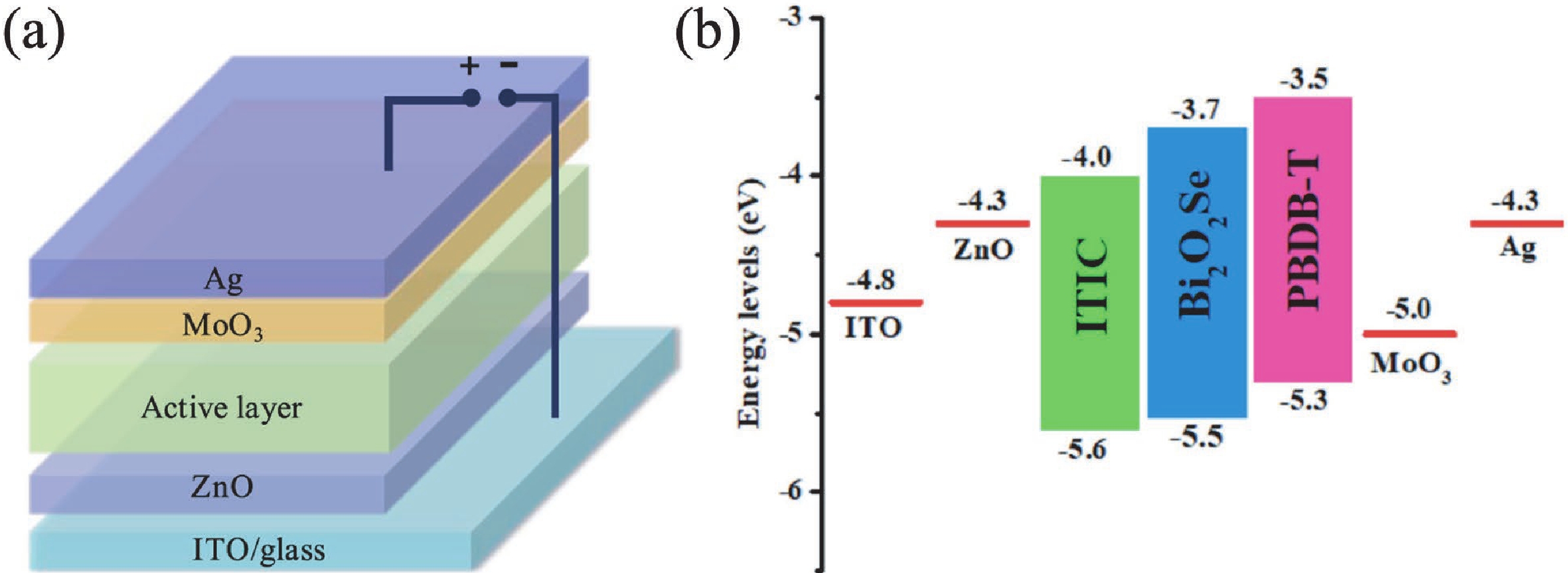
Huang C W, Yu H. 2D Bi 2O 2Se with high mobility for high performance polymer solar cells. ACS Appl Mater Interfaces, 2020, 12, 19643 doi: 10.1021/acsami.0c01364 |
| [80] |
Ding G L, Yang B D, Chen R S, et al. Reconfigurable 2D WSe 2-based memtransistor for mimicking homosynaptic and heterosynaptic plasticity. Small, 2021, 17, 2170213 doi: 10.1002/smll.202170213 |
| [81] |
Du J Y, Ge C, Riahi H, et al. Dual-gated MoS 2 transistors for synaptic and programmable logic functions. Adv Electron Mater, 2020, 6, 1901408 doi: 10.1002/aelm.201901408 |
| [82] |
Yang Q Y, Luo Z D, Zhang D W, et al. Controlled optoelectronic response in van der Waals heterostructures for In-sensor computing. Adv Funct Mater, 2022, 32(45), 202207290 doi: 10.1002/adfm.202207290 |
| [83] |
Yan J M, Ying J S, Yan M Y, et al. Optoelectronic coincidence detection with two-dimensional Bi 2O 2Se ferroelectric field-effect transistors. Adv Funct Mater, 2021, 31, 2103982 doi: 10.1002/adfm.202103982 |
| [84] |
Wang F K, Yang S J, Wu J, et al. Emerging two-dimensional bismuth oxychalcogenides for electronics and optoelectronics. InfoMat, 2021, 3, 1251 doi: 10.1002/inf2.12215 |
| [85] |
Li Z W, Li J S. Bi 2O 2Se for broadband terahertz wave switching. Appl Opt, 2020, 59, 11076 doi: 10.1364/AO.412728 |
| [86] |
Meng X D, Liu Z Q, Cao Y, et al. Cancer therapy: Fabricating aptamer-conjugated PEGylated-MoS 2/Cu 1.8S theranostic nanoplatform for multiplexed imaging diagnosis and chemo-photothermal therapy of cancer. Adv Funct Mater, 2017, 27, 1605592 doi: 10.1002/adfm.201605592 |
| [87] |
Chen Z, Zhao P F, Luo Z Y, et al. Cancer cell membrane-biomimetic nanoparticles for homologous-targeting dual-modal imaging and photothermal therapy. ACS Nano, 2016, 10, 10049 doi: 10.1021/acsnano.6b04695 |
| [88] |
Li B, Yuan F K, He G J, et al. Ultrasmall CuCo 2S 4 nanocrystals: All-in-one theragnosis nanoplatform with magnetic resonance/near-infrared imaging for efficiently photothermal therapy of tumors. Adv Funct Mater, 2017, 27, 1606218 doi: 10.1002/adfm.201606218 |
| [89] |
Wu M H, Zeng X C. Bismuth oxychalcogenides: A new class of ferroelectric/ferroelastic materials with ultra high mobility. Nano Lett, 2017, 17, 6309 doi: 10.1021/acs.nanolett.7b03020 |
| [90] |
Zhu Z Y, Yao X P, Zhao S, et al. Giant modulation of the electron mobility in semiconductor Bi 2O 2Se via incipient ferroelectric phase transition. J Am Chem Soc, 2022, 144, 4541 doi: 10.1021/jacs.1c12681 |


 DownLoad: