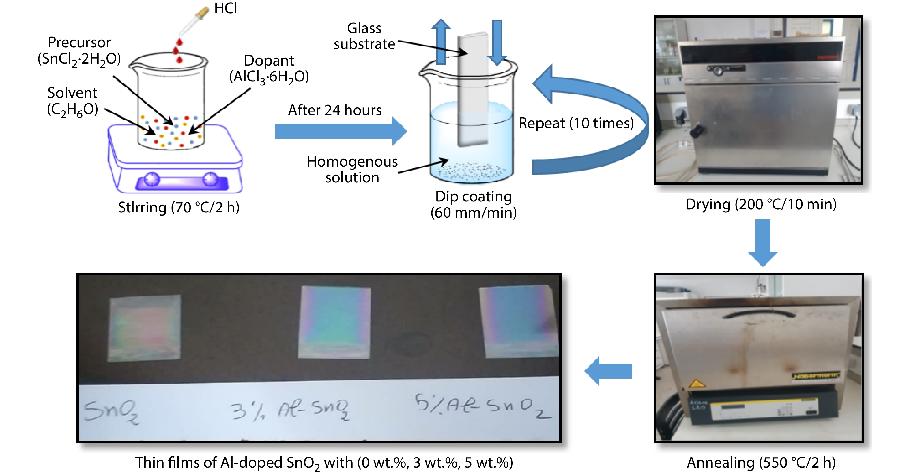
Fig. 1.
(Color online) The schematic drawing of pure and Al-doped SnO2 thin films produced with a sol-gel dip coating method.
ARTICLES
Kaour Selma1, 2, Benkara Salima3, 4, , Bouabida Seddik3, Rechem Djamil1, 3 and Hadjeris Lazhar1, 2
Corresponding author: Benkara Salima, sali_benkara@yahoo.fr
Abstract: Transparent conducting aluminum doped tin oxide thin films were prepared by sol-gel dip coating method with different Al concentrations and characterized by X-ray diffraction (XRD), atomic force microscopy (AFM), UV–Vis spectrophotometry and photoconductivity study. The variation observed in the properties of the measured films agrees with a difference in the film's thickness, which decreases when Al concentration augments. X-ray diffraction analysis reveals that all films are polycrystalline with tetragonal structure, (110) plane being the strongest diffraction peak. The crystallite size calculated by the Debye Scherrer’s formula decreases from 11.92 to 8.54 nm when Al concentration increases from 0 to 5 wt.%. AFM images showed grains uniformly distributed in the deposited films. An average transmittance greater than 80% was measured for the films and an energy gap value of about 3.9 eV was deduced from the optical analysis. Finally, the photosensitivity properties like current–voltage characteristics, ION/IOFF ratio, growth and decay time are studied and reported. Also, we have calculated the trap depth energy using the decay portion of the rise and decay curve photocurrent.
Key words: tin oxide, thin films, sol-gel, UV photodetector, photoconductivity, trap depth
| [1] |
Al-Zuhairi O, Shuhaimi A, Nayan N, et al. Non-polar gallium nitride for photodetection applications: A systematic review. Coatings, 2022, 12, 275 doi: 10.3390/coatings12020275
|
| [2] |
İlhan M, Koc M M, Coskun B, et al. Structural and optoelectronic characterization of Cu2CoSnS4 quaternary functional photodetectors. Optik, 2020, 212, 164724 doi: 10.1016/j.ijleo.2020.164724
|
| [3] |
Mishra S K, Bayan S, Shankar R, et al. Efficient UV photosensitive and photoluminescence properties of sol-gel derived Sn doped ZnO nanostructures. Sens Actuat A, 2014, 211, 8 doi: 10.1016/j.sna.2014.02.020
|
| [4] |
Liu H Y, Lin W X, Sun W Q, et al. A study of ultrasonic spray pyrolysis deposited rutile-TiO2-based metal-semiconductor-metal ultraviolet photodetector. Mater Sci Semicond Process, 2017, 57, 90 doi: 10.1016/j.mssp.2016.10.005
|
| [5] |
Khayatian A, Kashi M A, Azimrad R, et al. Effect of annealing process in tuning of defects in ZnO nanorods and their application in UV photodetectors. Optik, 2016, 127, 4675 doi: 10.1016/j.ijleo.2016.01.177
|
| [6] |
Oshima T, Okuno T, Fujita S. UV-B sensor based on a SnO2 thin film. Jpn J Appl Phys, 2009, 48, 120207 doi: 10.1143/JJAP.48.120207
|
| [7] |
Leem J W, Yu J S. Physical properties of electrically conductive Sb-doped SnO2 transparent electrodes by thermal annealing dependent structural changes for photovoltaic applications. Mater Sci Eng B, 2011, 176, 1207 doi: 10.1016/j.mseb.2011.06.015
|
| [8] |
Song P, Wang Q, Yang Z X. Preparation, characterization and acetone sensing properties of Ce-doped SnO2 hollow spheres. Sens Actuat B, 2012, 173, 839 doi: 10.1016/j.snb.2012.07.115
|
| [9] |
Khan A F, Mehmood M, Aslam M, et al. Characteristics of electron beam evaporated nanocrystalline SnO2 thin films annealed in air. Appl Surf Sci, 2010, 256, 2252 doi: 10.1016/j.apsusc.2009.10.047
|
| [10] |
Kumari N, Ghosh A, Tewari S, et al. Synthesis, structural and optical properties of Al doped SnO2 nanoparticles. Indian J Phys, 2014, 88, 65 doi: 10.1007/s12648-013-0387-0
|
| [11] |
Sivasankar Reddy A, Figueiredo N M, Cavaleiro A. Nanocrystalline Au:Ag:SnO2 films prepared by pulsed magnetron sputtering. J Phys Chem Solids, 2013, 74, 825 doi: 10.1016/j.jpcs.2013.01.023
|
| [12] |
Dien E, Laurent J M, Smith A, et al. Comparison of optical and electrical characteristics of SnO2-based thin films deposited by pyrosol from different tin precursors. J Eur Ceram Soc, 1999, 19, 787 doi: 10.1016/S0955-2219(98)00313-6
|
| [13] |
Tran Q P, Fang J S, Chin T S. Optical properties and boron doping-induced conduction-type change in SnO2 thin films. J Electron Mater, 2016, 45, 349 doi: 10.1007/s11664-015-4081-1
|
| [14] |
Bonu V, Das A, Amirthapandian S, et al. Photoluminescence of oxygen vacancies and hydroxyl group surface functionalized SnO2 nanoparticles. Phys Chem Chem Phys, 2015, 17, 9794 doi: 10.1039/C5CP00060B
|
| [15] |
Moazzami K, Murphy T E, Phillips J D, et al. Sub-bandgap photoconductivity in ZnO epilayers and extraction of trap density spectra. Semicond Sci Technol, 2006, 21, 717 doi: 10.1088/0268-1242/21/6/001
|
| [16] |
Brinzari V. Mechanism of band gap persistent photoconductivity (PPC) in SnO2 nanoscrystalline films: Nature of local states, simulation of PPC and comparison with experiment. Appl Surf Sci, 2017, 411, 437 doi: 10.1016/j.apsusc.2017.03.209
|
| [17] |
Mishra S K, Srivastava S, Srivastava R K, et al. Photoluminescence and ultraviolet photoresponse in ZnO nanophorsphors prepared by thermal decomposition of zinc acetate. Adv Mater Lett, 2011, 2, 298 doi: 10.5185/amlett.indias.210
|
| [18] |
Mishra S K, Srivastava R K, Prakash S G, et al. Photoluminescence and photoconductive characteristics of hydrothermally synthesized ZnO nanoparticles. Opto-Electron Rev, 2010, 18, 467 doi: 10.2478/s11772-010-0037-4
|
| [19] |
Ku C J, Reyes P, Duan Z Q, et al. Mg xZn1− xO thin-film transistor-based UV photodetectorwith enhanced photoresponse. J Electron Mater, 2015, 44, 3471 doi: 10.1007/s11664-015-3697-5
|
| [20] |
Huang S Y, Matsubara K, Cheng J, et al. Highly enhanced ultraviolet photosensitivity and recovery speed in electrospun Ni-doped SnO2 nanobelts. Appl Phys Lett, 2013, 103, 141108 doi: 10.1063/1.4824026
|
| [21] |
Kumar M, Bhatt V, Abhyankar A C, et al. Modulation of structural properties of Sn doped ZnO for UV photoconductors. Sens Actuat A, 2018, 270, 118 doi: 10.1016/j.sna.2017.12.045
|
| [22] |
Akin N, Baskose U C, Kinaci B, et al. AZO thin film-based UV sensors: Effects of RF power on the films. Appl Phys A, 2015, 119, 965 doi: 10.1007/s00339-015-9051-1
|
| [23] |
Singh S. Simulation, fabrication, and characterization of Al-doped ZnO-based ultraviolet photodetectors. J Electron Mater, 2016, 45, 535 doi: 10.1007/s11664-015-4144-3
|
| [24] |
Mahroug A, Boudjadar S, Hamritet S, al. Structural, optical and photocurrent properties of undoped and Al-doped ZnO thin films deposited by sol-gel spin coating technique. Mater Lett, 2014, 134, 248 doi: 10.1016/j.matlet.2014.07.099
|
| [25] |
Inamdar S I, Ganbavle V V, Rajpure K Y. ZnO based visible-blind UV photodetector by spray pyrolysis. Superlattices Microstruct, 2014, 76, 253 doi: 10.1016/j.spmi.2014.09.041
|
| [26] |
Shaikh S K, Inamdar S I, Ganbavle V V, et al. Chemical bath deposited ZnO thin film based UV photoconductive detector. J Alloys Compd, 2016, 664, 242 doi: 10.1016/j.jallcom.2015.12.226
|
| [27] |
Gurakar S, Serin T, Serin N. Electrical and microstructural properties of (Cu, Al, In)-doped SnO2 films deposited by spray pyrolysis. Adv Mater Lett, 2014, 5, 309 doi: 10.5185/amlett.2014.amwc.1016
|
| [28] |
Lekshmy S S, Daniel G P, Joy K. Microstructure and physical properties of sol gel derived SnO2: Sb thin films for optoelectronic applications. Appl Surf Sci, 2013, 274, 95 doi: 10.1016/j.apsusc.2013.02.109
|
| [29] |
Djamil R, Aicha K, Souifi A, et al. Effect of annealing time on the performance of tin oxide thin films ultraviolet photodetectors. Thin Solid Films, 2017, 623, 1 doi: 10.1016/j.tsf.2016.12.035
|
| [30] |
Bhorde A, Waykar R, Nair S, et al. Room temperature synthesis of transparent and conducting indium tin oxide films with high mobility and figure of merit by RF-magnetron sputtering. J Electron Mater, 2019, 48, 7192 doi: 10.1007/s11664-019-07533-8
|
| [31] |
He L N, Cao Q, Feng X J, et al. Structural, optical and electrical properties of epitaxial rutile SnO2 films grown on MgF2 (110) substrates by MOCVD. Ceram Int, 2018, 44, 869 doi: 10.1016/j.ceramint.2017.10.013
|
| [32] |
Abdelkrim A, Rahmane S, Ouahab Abdelouahab O, et al. Effect of solution concentration on the structural, optical and electrical properties of SnO2 thin films prepared by spray pyrolysis. Optik, 2016, 127, 2653 doi: 10.1016/j.ijleo.2015.11.232
|
| [33] |
Al-Jawad S M H. Influence of multilayer deposition on characteristics of nanocrystalline SnO2 thin films produce by Sol-gel technique for gas sensor application. Optik, 2017, 146, 17 doi: 10.1016/j.ijleo.2017.08.053
|
| [34] |
Ammar A H, Abo-Ghazala M S, Farag A A M, et al. Effect of gas type, pressure and temperature on the electrical characteristics of Al-doped SnO2 thin films deposited by RGTO method for gas sensor application. Vacuum, 2013, 94, 30 doi: 10.1016/j.vacuum.2013.01.013
|
| [35] |
Chen H, Liu D T, Wang Y F, et al. Enhanced performance of planar perovskite solar cells using low-temperature solution-processed Al-doped SnO2 as electron transport layers. Nanoscale Res Lett, 2017, 12, 238 doi: 10.1186/s11671-017-1992-1
|
| [36] |
Bouznit Y, Henni A. Characterization of Sb doped SnO2 films prepared by spray technique and their application to photocurrent generation. Mater Chem Phys, 2019, 233, 242 doi: 10.1016/j.matchemphys.2019.05.072
|
| [37] |
Zhelev V, Petkov P, P. Shindov P, et al As-doped SnO2 thin films for use as large area position sensitive photodetector. Thin Solid Films, 2018, 653, 19 doi: 10.1016/j.tsf.2018.03.009
|
| [38] |
Aldemir D A, Benhaliliba M, Benouis C E, et al. Photodiode based on Al-doped SnO2: Fabrication, current-voltage and capacitance-conductance-voltage measurements. Optik, 2020, 222, 165487 doi: 10.1016/j.ijleo.2020.165487
|
| [39] |
Marimuthu G, Saravanakumar K, Jeyadheepan K, et al. Influence of twin boundaries on the photocurrent decay of nanobranch and dense-forest structured SnO2 UV photodetectors. Superlattices Microstruct, 2019, 128, 181 doi: 10.1016/j.spmi.2019.01.032
|
| [40] |
Wu J J, Huang Q W, Zeng D W, et al. Al-doping induced formation of oxygen-vacancy for enhancing gas-sensing properties of SnO2 NTs by electrospinning. Sens Actuat B, 2014, 198, 62 doi: 10.1016/j.snb.2014.03.012
|
| [41] |
Ahmed S F, Ghosh P K, Khan S, et al. Low-macroscopic field emission from nanocrystalline Al doped SnO2 thin films synthesized by Sol-gel technique. Appl Phys A, 2007, 86, 139 doi: 10.1007/s00339-006-3734-6
|
| [42] |
Rahal A, Benhaoua A, Bouzidi C, et al. Effect of antimony doping on the structural, optical and electrical properties of SnO2 thin films prepared by spray ultrasonic. Superlattices Microstruct, 2014, 76, 105 doi: 10.1016/j.spmi.2014.09.024
|
| [43] |
Sinha S K, Ray S K, Manna I. Effect of Al doping on structural, optical and electrical properties of SnO2 thin films synthesized by pulsed laser deposition. Philos Mag, 2014, 94, 3507 doi: 10.1080/14786435.2014.962641
|
| [44] |
Soumya S S, Vinodkumar R, Unnikrishnan N V. Conductivity type inversion and optical properties of aluminium doped SnO2 thin films prepared by sol-gel spin coating technique. J Sol-Gel Sci Technol, 2021, 99, 636 doi: 10.1007/s10971-021-05599-7
|
| [45] |
Sujatha K, Seethalakshmi T, Sudha A P, et al. Photocatalytic activity of pure, Zn doped and surfactants assisted Zn doped SnO2 nanoparticles for degradation of cationic dye. Nano Struct Nano Objects, 2019, 18, 100305 doi: 10.1016/j.nanoso.2019.100305
|
| [46] |
El Sayed A M, Taha S, Shaban M, et al. Tuning the structural, electrical and optical properties of tin oxide thin films via cobalt doping and annealing. Superlattices Microstruct, 2016, 95, 1 doi: 10.1016/j.spmi.2016.04.017
|
| [47] |
Sivakumar P, Akkera H S, Reddy T R K, et al. Effect of Ti doping on structural, optical and electrical properties of SnO2 transparent conducting thin films deposited by sol-gel spin coating. Opt Mater, 2021, 113, 110845 doi: 10.1016/j.optmat.2021.110845
|
| [48] |
Lin Z D, Li N, Chen Z, et al. The effect of Ni doping concentration on the gas sensing properties of Ni doped SnO2. Sens Actuat B, 2017, 239, 501 doi: 10.1016/j.snb.2016.08.053
|
| [49] |
Korotkov R Y, Ricou P, Farran A J E. Preferred orientations in polycrystalline SnO2 films grown by atmospheric pressure chemical vapor deposition. Thin Solid Films, 2006, 502, 79 doi: 10.1016/j.tsf.2005.07.248
|
| [50] |
Kim C Y, Riu D H. Texture control of fluorine-doped tin oxide thin film. Thin Solid Films, 2011, 519, 3081 doi: 10.1016/j.tsf.2010.12.096
|
| [51] |
Wang J T, Shi X L, Zhong X H, et al. Morphology control of fluorine-doped tin oxide thin films for enhanced light trapping. Sol Energy Mater Sol Cells, 2015, 132, 578 doi: 10.1016/j.solmat.2014.09.043
|
| [52] |
Teldja B, Noureddine B, Azzeddine B, et al. Effect of indium doping on the UV photoluminescence emission, structural, electrical and optical properties of spin-coating deposited SnO2 thin films. Optik, 2020, 209, 164586 doi: 10.1016/j.ijleo.2020.164586
|
| [53] |
Reddy N N K, Akkera H S, Sekhar M C, et al. Zr-doped SnO2 thin films synthesized by spray pyrolysis technique for barrier layers in solar cells. Appl Phys A, 2017, 123, 761 doi: 10.1007/s00339-017-1391-6
|
| [54] |
Yang Y Z, Zhou W, Liang Y H, et al. Tuning band gap and ferromagnetism in epitaxial Al-doped SnO2 films by defect engineering. J Cryst Growth, 2015, 430, 75 doi: 10.1016/j.jcrysgro.2015.08.021
|
| [55] |
Baig F, Ashraf M W, Asif A, et al. A comparative analysis for effects of solvents on optical properties of Mg doped ZnO thin films for optoelectronic applications. Optik, 2020, 208, 164534 doi: 10.1016/j.ijleo.2020.164534
|
| [56] |
Bagheri-Mohagheghi M M, Shokooh-Saremi M. The influence of Al doping on the electrical, optical and structural properties of SnO2 transparent conducting films deposited by the spray pyrolysis technique. J Phys D, 2004, 37, 1248 doi: 10.1088/0022-3727/37/8/014
|
| [57] |
Benouis C E, Benhaliliba M, Z. Mouffak Z, et al The low resistive and transparent Al-doped SnO2 films: P-type conductivity, nanostructures and photoluminescence. J Alloys Compd, 2014, 603, 213 doi: 10.1016/j.jallcom.2014.03.046
|
| [58] |
Smith R W, Rose A. Space-charge-limited Currents in single crystals of cadmium sulfide. Phys Rev, 1955, 97, 1531 doi: 10.1103/PhysRev.97.1531
|
| [59] |
Mishra S K, Srivastava R K, Prakash S G. ZnO nanoparticles: Structural, optical and photoconductivity characteristics. J Alloys Compd, 2012, 539, 1 doi: 10.1016/j.jallcom.2012.06.024
|
| [60] |
Shankar R, Srivastava R K. Photoconductivity and luminescence properties of gadolinium doped zinc oxide. Proc Natl Acad Sci, India, Sect A Phys Sci, 2018, 88, 137 doi: 10.1007/s40010-016-0328-3
|
| [61] |
Farooqi M M H, Srivastava R K. Effect of annealing temperature on structural, photoluminescence and photoconductivity properties of ZnO thin film deposited on glass substrate by sol-gel spin coating method. Proc Natl Acad Sci India Sect A Phys Sci, 2020, 90, 845 doi: 10.1007/s40010-019-00648-x
|
| [62] |
Agrahari V, Mathpal M C, Kumar M, et al. Investigations of optoelectronic properties in DMS SnO2 nanoparticles. J Alloys Compd, 2015, 622, 48 doi: 10.1016/j.jallcom.2014.10.009
|
| [63] |
Kim D, Leem J Y. Morphology changes of In-doped ZnO nanosheets via ZnCl2 and InCl3 vapor formation during thermal dissipation annealing process and improved UV photoresponse properties. J Alloys Compd, 2021, 877, 160241 doi: 10.1016/j.jallcom.2021.160241
|
| [64] |
Kim J M, Lim S J, Nam T, et al. The effects of ultraviolet exposure on the device characteristics of atomic layer deposited-ZnO:N thin film transistors. J Electrochem Soc, 2011, 158, J150 doi: 10.1149/1.3560191
|
| [65] |
Yang T T, Sun B, Ni L, et al. The mechanism of photocurrent enhancement of ZnO ultraviolet photodetector by reduced graphene oxide. Curr Appl Phys, 2018, 18, 859 doi: 10.1016/j.cap.2018.04.010
|
| [66] |
Zhou W Q, Yao G Y, Chen L J, et al. Pretreatment hematocrit is negatively associated with response to neoadjuvant chemotherapy in breast cancer. Biomark Med, 2017, 11, 713 doi: 10.2217/bmm-2017-0054
|
| [67] |
Gröttrup J, Postica V, Smazna D, et al. UV detection properties of hybrid ZnO tetrapod 3-D networks. Vacuum, 2017, 146, 492 doi: 10.1016/j.vacuum.2017.03.017
|
| [68] |
Kumar N, Srivastava A. Green photoluminescence and photoconductivity from screen-printed Mg doped ZnO films. J Alloys Compd, 2018, 735, 312 doi: 10.1016/j.jallcom.2017.11.024
|
| [69] |
Ghosh T, Basak D. Highly enhanced ultraviolet photoresponse property in Cu-doped and Cu-Li co-doped ZnO films. J Phys D, 2009, 42, 145304 doi: 10.1088/0022-3727/42/14/145304
|
| [70] |
Rose A. Space-charge-limited Currents in solids. Phys Rev, 1955, 97, 1538 doi: 10.1103/PhysRev.97.1538
|
| [71] |
Randall J T, Wilkins M H F. Phosphorescence and electron traps - I. The study of trap distributions. Proc R Soc Lond A, 1945, 184, 365 doi: 10.1098/rspa.1945.0024
|
| [72] |
Gupta A, Verma N K, Bhatti H S. Fast photoluminescence decay processes of doped ZnO phosphors. Appl Phys B, 2007, 87, 311 doi: 10.1007/s00340-007-2582-1
|
| [73] |
Agrahari V, Tripathi A K, Mathpal M C, et al. Effect of Mn doping on structural, optical and magnetic properties of SnO2 nanoparticles. J Mater Sci: Mater Electron, 2015, 26, 9571 doi: 10.1007/s10854-015-3620-0
|
| [74] |
Kong J T, Zheng W, Liu Y S, et al. Persistent luminescence from Eu3+ in SnO2 nanoparticles. Nanoscale, 2015, 7, 11048 doi: 10.1039/C5NR01961C
|
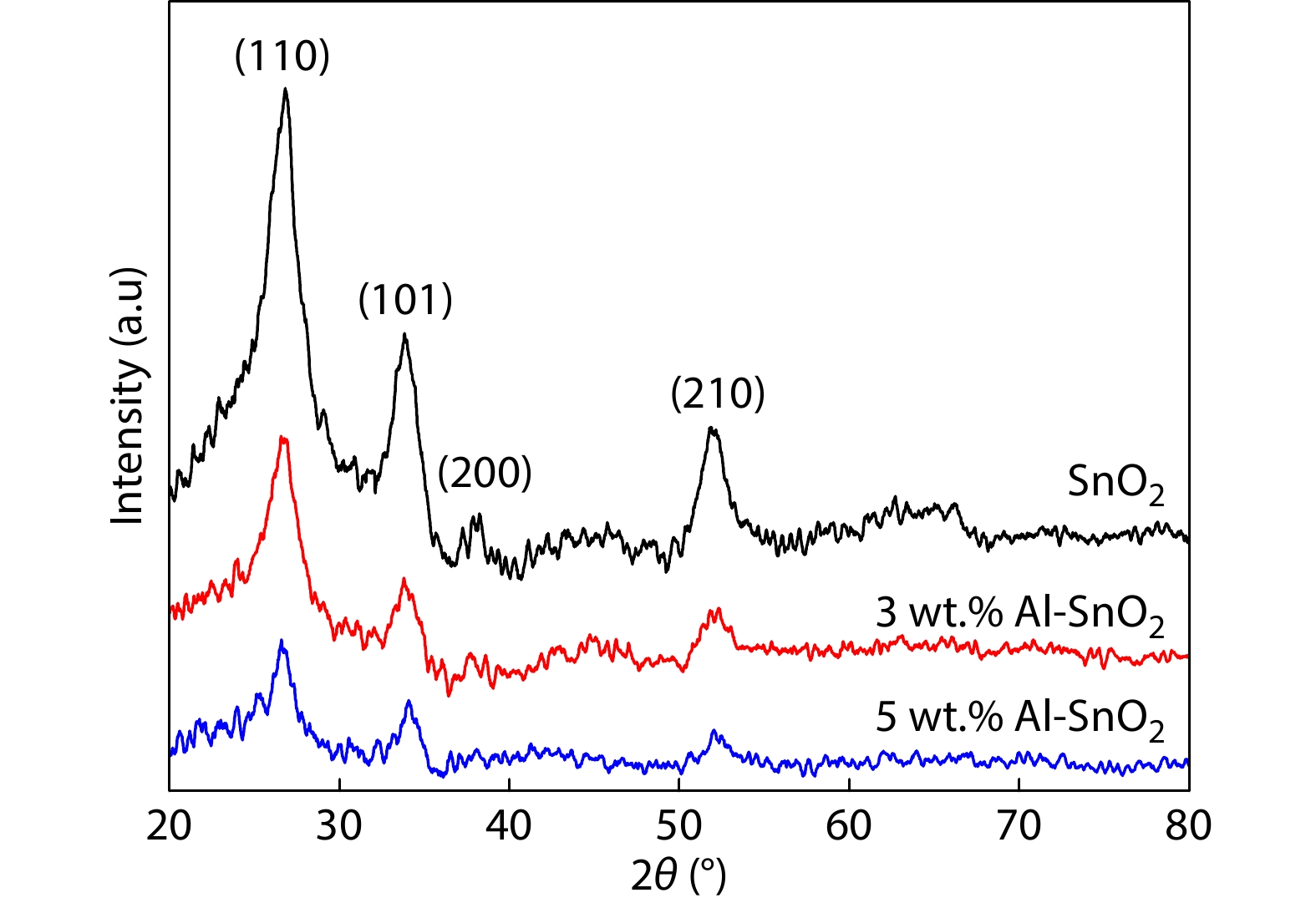
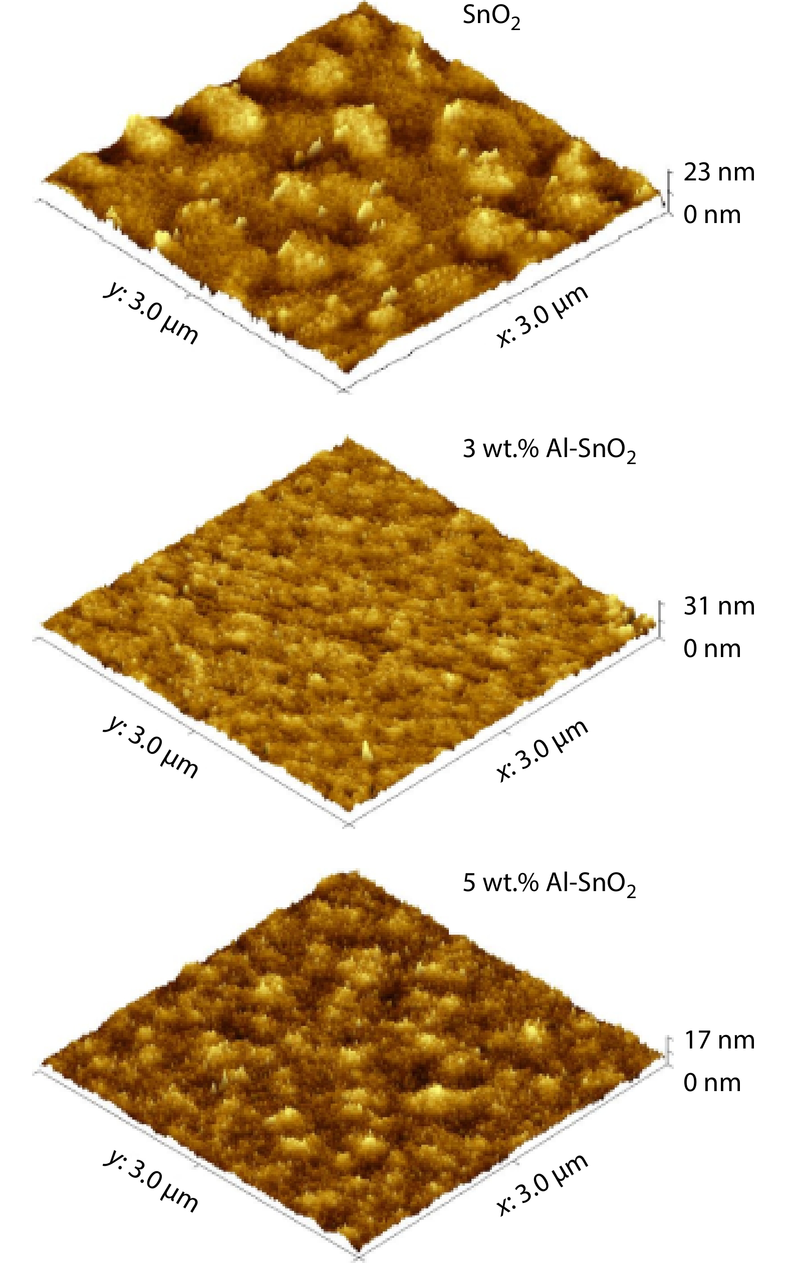
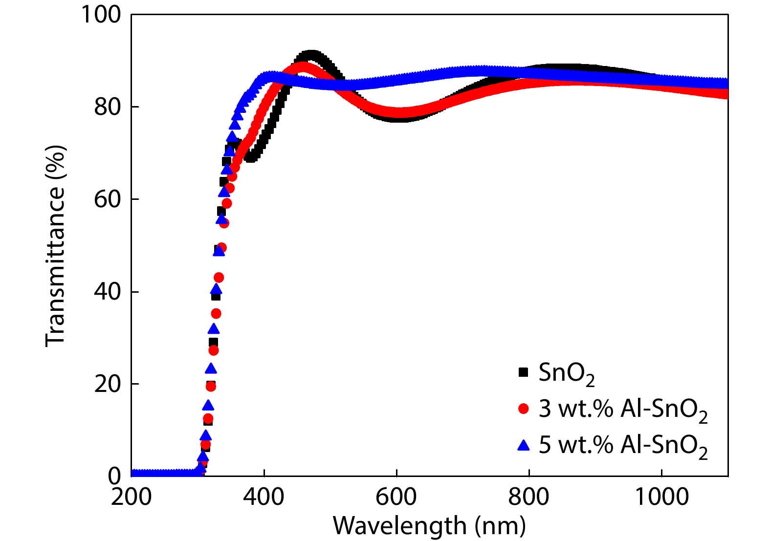
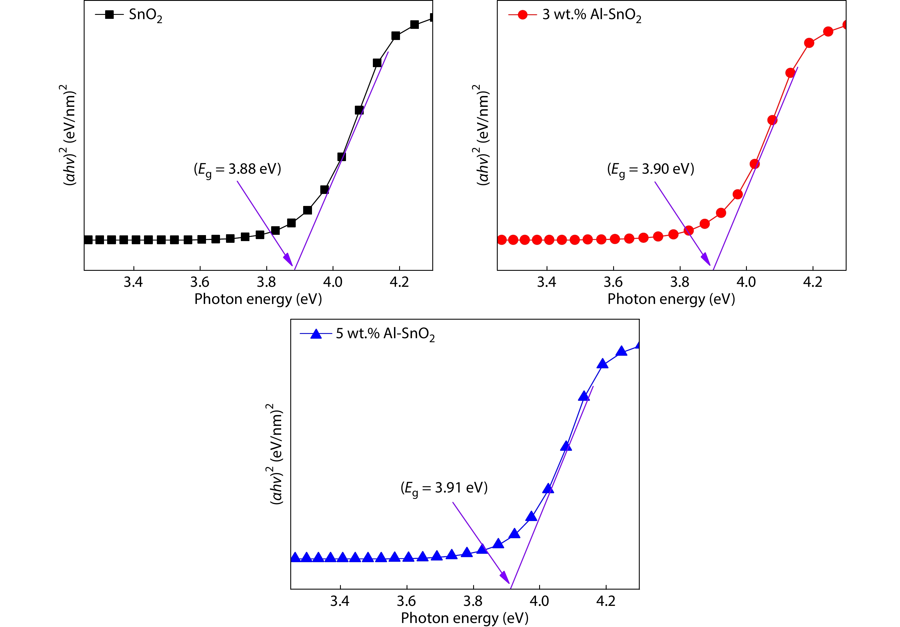
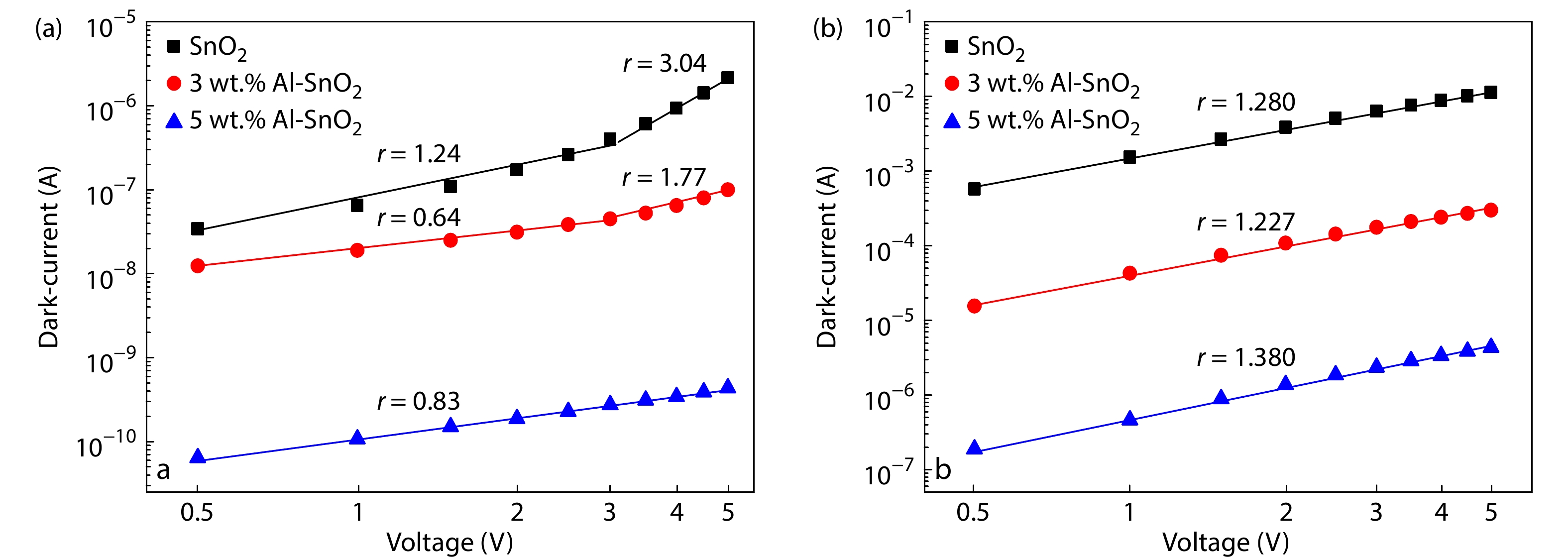

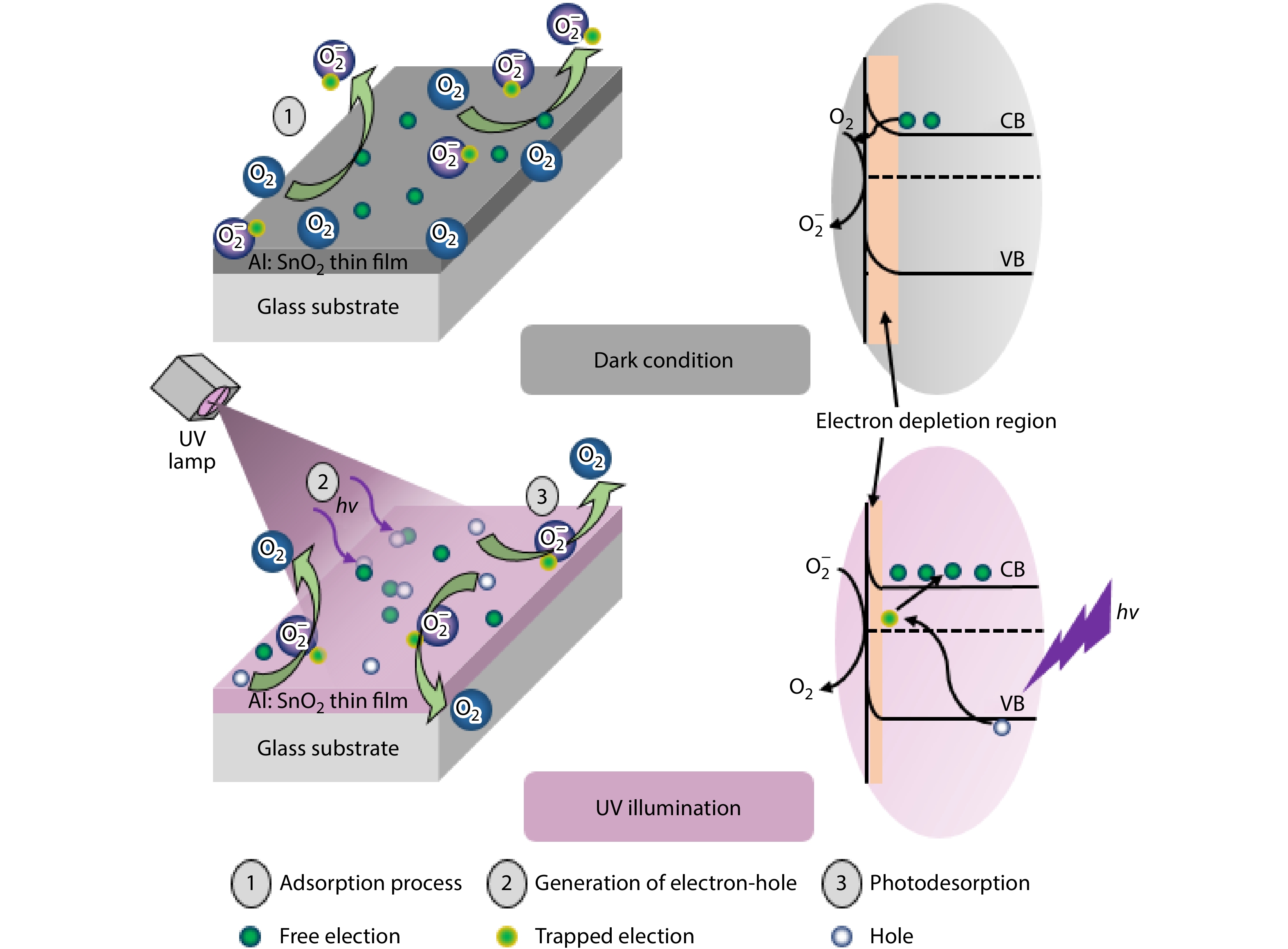
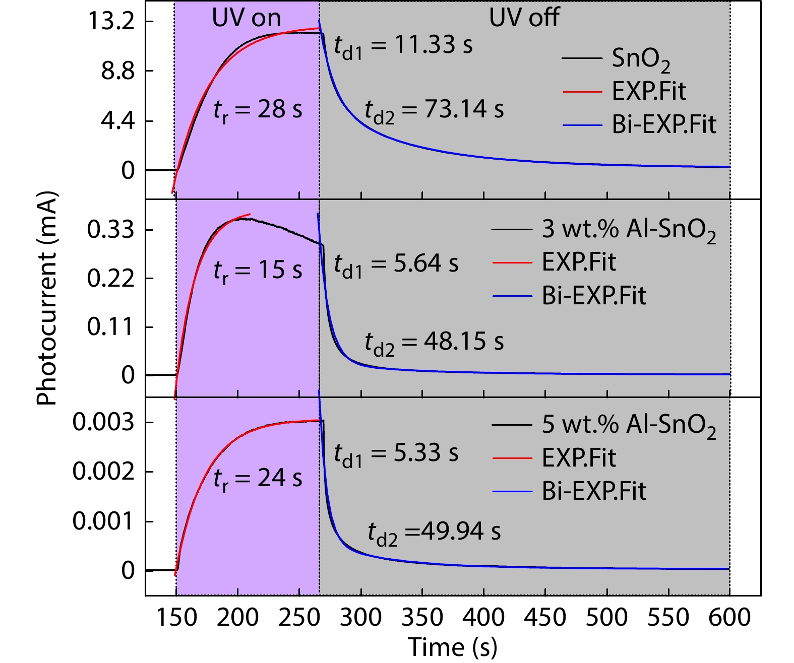
Table 1. XRD parameters, crystallite size, strain and RMS of undoped and Al-doped SnO2 thin films.
| Sample | 2θ (°) | Β (°) | D (nm) | Strain (10−3) | $a$ = b (Å) | c (Å) | RMS (nm) | Ra (nm) | Da (nm) |
| SnO2 | 26.79 | 0.71 | 11.92 | 3.27 | 4.700 | 3.203 | 5.06 | 4.25 | 73.0 |
| 3 wt.% Al-SnO2 | 26.56 | 0.74 | 11.40 | 3.42 | 4.742 | 3.195 | 2.32 | 1.76 | 45.5 |
| 5 wt.% Al-SnO2 | 26.58 | 0.99 | 08.54 | 4.60 | 4.738 | 3.161 | 2.01 | 1.67 | 29.3 |
 DownLoad: CSV
Table 2. The values of Texture Coefficient of undopedand Al-doped SnO2 thin films.
| Sample | Tc(hkl) of SnO2 thin films | |||
| (110) | (101) | (200) | (210) | |
| SnO2 | 1.22 | 1.17 | 0.78 | 0.83 |
| 3 wt.% Al-SnO2 | 1.41 | 0.94 | 0.86 | 0.77 |
| 5 wt.% Al-SnO2 | 1.33 | 1.12 | 0.62 | 0.91 |
DownLoad: CSV
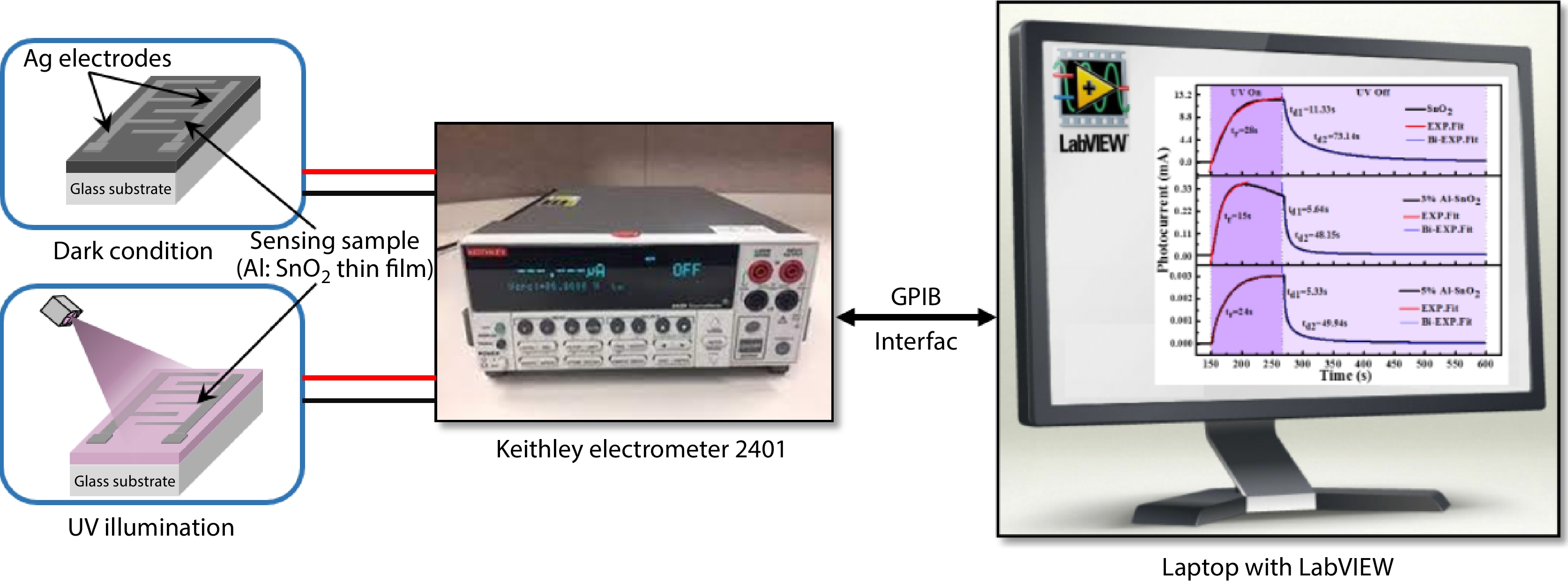
Table 3. The values of photocurrent, dark current, ION/IOFF ratio, rise time constant (tr), decay time constants (td1, td2) and defect levels energy (trap depth (E1, E2)) for undoped and Al-doped SnO2 thin films.
| Sample | ION (A) | IOFF (A) | ION/IOFF | tr (s) | td1 (s) | td2 (s) | E1 (eV) | E2 (eV) | Ref. |
| SnO2 | 1.22 × 10⁻² | 7.75 × 10⁻⁵ | 217.85 | 28 | 11.33 | 73.14 | 0.598 | 0.64 | This work |
| 3 wt.% Al-SnO2 | 3.56 × 10⁻⁴ | 1.30 × 10⁻⁶ | 273.84 | 15 | 5.64 | 48.15 | 0.580 | 0.63 | This work |
| 5 wt.% Al-SnO2 | 3.03 × 10⁻⁶ | 1.95 × 10⁻⁸ | 155.38 | 24 | 5.33 | 49.94 | 0.579 | 0.63 | This work |
| Mg-ZnO films | – | – | 8.49 | 196 | 14.3 | 112.1 | 0.640 | 0.70 | [68] |
| Cu/LiZnO | 9.6 × 10⁻¹¹ | 1.20 × 10⁻⁷ | 1250 | 769 | 35 | 222 | – | – | [69] |
| SnO2 films | 3.2×10⁻¹¹ | 1.43 × 10⁻⁹ | 44 | 250 | 506 | – | – | – | [39] |
DownLoad: CSV
| [1] |
Al-Zuhairi O, Shuhaimi A, Nayan N, et al. Non-polar gallium nitride for photodetection applications: A systematic review. Coatings, 2022, 12, 275 doi: 10.3390/coatings12020275
|
| [2] |
İlhan M, Koc M M, Coskun B, et al. Structural and optoelectronic characterization of Cu2CoSnS4 quaternary functional photodetectors. Optik, 2020, 212, 164724 doi: 10.1016/j.ijleo.2020.164724
|
| [3] |
Mishra S K, Bayan S, Shankar R, et al. Efficient UV photosensitive and photoluminescence properties of sol-gel derived Sn doped ZnO nanostructures. Sens Actuat A, 2014, 211, 8 doi: 10.1016/j.sna.2014.02.020
|
| [4] |
Liu H Y, Lin W X, Sun W Q, et al. A study of ultrasonic spray pyrolysis deposited rutile-TiO2-based metal-semiconductor-metal ultraviolet photodetector. Mater Sci Semicond Process, 2017, 57, 90 doi: 10.1016/j.mssp.2016.10.005
|
| [5] |
Khayatian A, Kashi M A, Azimrad R, et al. Effect of annealing process in tuning of defects in ZnO nanorods and their application in UV photodetectors. Optik, 2016, 127, 4675 doi: 10.1016/j.ijleo.2016.01.177
|
| [6] |
Oshima T, Okuno T, Fujita S. UV-B sensor based on a SnO2 thin film. Jpn J Appl Phys, 2009, 48, 120207 doi: 10.1143/JJAP.48.120207
|
| [7] |
Leem J W, Yu J S. Physical properties of electrically conductive Sb-doped SnO2 transparent electrodes by thermal annealing dependent structural changes for photovoltaic applications. Mater Sci Eng B, 2011, 176, 1207 doi: 10.1016/j.mseb.2011.06.015
|
| [8] |
Song P, Wang Q, Yang Z X. Preparation, characterization and acetone sensing properties of Ce-doped SnO2 hollow spheres. Sens Actuat B, 2012, 173, 839 doi: 10.1016/j.snb.2012.07.115
|
| [9] |
Khan A F, Mehmood M, Aslam M, et al. Characteristics of electron beam evaporated nanocrystalline SnO2 thin films annealed in air. Appl Surf Sci, 2010, 256, 2252 doi: 10.1016/j.apsusc.2009.10.047
|
| [10] |
Kumari N, Ghosh A, Tewari S, et al. Synthesis, structural and optical properties of Al doped SnO2 nanoparticles. Indian J Phys, 2014, 88, 65 doi: 10.1007/s12648-013-0387-0
|
| [11] |
Sivasankar Reddy A, Figueiredo N M, Cavaleiro A. Nanocrystalline Au:Ag:SnO2 films prepared by pulsed magnetron sputtering. J Phys Chem Solids, 2013, 74, 825 doi: 10.1016/j.jpcs.2013.01.023
|
| [12] |
Dien E, Laurent J M, Smith A, et al. Comparison of optical and electrical characteristics of SnO2-based thin films deposited by pyrosol from different tin precursors. J Eur Ceram Soc, 1999, 19, 787 doi: 10.1016/S0955-2219(98)00313-6
|
| [13] |
Tran Q P, Fang J S, Chin T S. Optical properties and boron doping-induced conduction-type change in SnO2 thin films. J Electron Mater, 2016, 45, 349 doi: 10.1007/s11664-015-4081-1
|
| [14] |
Bonu V, Das A, Amirthapandian S, et al. Photoluminescence of oxygen vacancies and hydroxyl group surface functionalized SnO2 nanoparticles. Phys Chem Chem Phys, 2015, 17, 9794 doi: 10.1039/C5CP00060B
|
| [15] |
Moazzami K, Murphy T E, Phillips J D, et al. Sub-bandgap photoconductivity in ZnO epilayers and extraction of trap density spectra. Semicond Sci Technol, 2006, 21, 717 doi: 10.1088/0268-1242/21/6/001
|
| [16] |
Brinzari V. Mechanism of band gap persistent photoconductivity (PPC) in SnO2 nanoscrystalline films: Nature of local states, simulation of PPC and comparison with experiment. Appl Surf Sci, 2017, 411, 437 doi: 10.1016/j.apsusc.2017.03.209
|
| [17] |
Mishra S K, Srivastava S, Srivastava R K, et al. Photoluminescence and ultraviolet photoresponse in ZnO nanophorsphors prepared by thermal decomposition of zinc acetate. Adv Mater Lett, 2011, 2, 298 doi: 10.5185/amlett.indias.210
|
| [18] |
Mishra S K, Srivastava R K, Prakash S G, et al. Photoluminescence and photoconductive characteristics of hydrothermally synthesized ZnO nanoparticles. Opto-Electron Rev, 2010, 18, 467 doi: 10.2478/s11772-010-0037-4
|
| [19] |
Ku C J, Reyes P, Duan Z Q, et al. Mg xZn1− xO thin-film transistor-based UV photodetectorwith enhanced photoresponse. J Electron Mater, 2015, 44, 3471 doi: 10.1007/s11664-015-3697-5
|
| [20] |
Huang S Y, Matsubara K, Cheng J, et al. Highly enhanced ultraviolet photosensitivity and recovery speed in electrospun Ni-doped SnO2 nanobelts. Appl Phys Lett, 2013, 103, 141108 doi: 10.1063/1.4824026
|
| [21] |
Kumar M, Bhatt V, Abhyankar A C, et al. Modulation of structural properties of Sn doped ZnO for UV photoconductors. Sens Actuat A, 2018, 270, 118 doi: 10.1016/j.sna.2017.12.045
|
| [22] |
Akin N, Baskose U C, Kinaci B, et al. AZO thin film-based UV sensors: Effects of RF power on the films. Appl Phys A, 2015, 119, 965 doi: 10.1007/s00339-015-9051-1
|
| [23] |
Singh S. Simulation, fabrication, and characterization of Al-doped ZnO-based ultraviolet photodetectors. J Electron Mater, 2016, 45, 535 doi: 10.1007/s11664-015-4144-3
|
| [24] |
Mahroug A, Boudjadar S, Hamritet S, al. Structural, optical and photocurrent properties of undoped and Al-doped ZnO thin films deposited by sol-gel spin coating technique. Mater Lett, 2014, 134, 248 doi: 10.1016/j.matlet.2014.07.099
|
| [25] |
Inamdar S I, Ganbavle V V, Rajpure K Y. ZnO based visible-blind UV photodetector by spray pyrolysis. Superlattices Microstruct, 2014, 76, 253 doi: 10.1016/j.spmi.2014.09.041
|
| [26] |
Shaikh S K, Inamdar S I, Ganbavle V V, et al. Chemical bath deposited ZnO thin film based UV photoconductive detector. J Alloys Compd, 2016, 664, 242 doi: 10.1016/j.jallcom.2015.12.226
|
| [27] |
Gurakar S, Serin T, Serin N. Electrical and microstructural properties of (Cu, Al, In)-doped SnO2 films deposited by spray pyrolysis. Adv Mater Lett, 2014, 5, 309 doi: 10.5185/amlett.2014.amwc.1016
|
| [28] |
Lekshmy S S, Daniel G P, Joy K. Microstructure and physical properties of sol gel derived SnO2: Sb thin films for optoelectronic applications. Appl Surf Sci, 2013, 274, 95 doi: 10.1016/j.apsusc.2013.02.109
|
| [29] |
Djamil R, Aicha K, Souifi A, et al. Effect of annealing time on the performance of tin oxide thin films ultraviolet photodetectors. Thin Solid Films, 2017, 623, 1 doi: 10.1016/j.tsf.2016.12.035
|
| [30] |
Bhorde A, Waykar R, Nair S, et al. Room temperature synthesis of transparent and conducting indium tin oxide films with high mobility and figure of merit by RF-magnetron sputtering. J Electron Mater, 2019, 48, 7192 doi: 10.1007/s11664-019-07533-8
|
| [31] |
He L N, Cao Q, Feng X J, et al. Structural, optical and electrical properties of epitaxial rutile SnO2 films grown on MgF2 (110) substrates by MOCVD. Ceram Int, 2018, 44, 869 doi: 10.1016/j.ceramint.2017.10.013
|
| [32] |
Abdelkrim A, Rahmane S, Ouahab Abdelouahab O, et al. Effect of solution concentration on the structural, optical and electrical properties of SnO2 thin films prepared by spray pyrolysis. Optik, 2016, 127, 2653 doi: 10.1016/j.ijleo.2015.11.232
|
| [33] |
Al-Jawad S M H. Influence of multilayer deposition on characteristics of nanocrystalline SnO2 thin films produce by Sol-gel technique for gas sensor application. Optik, 2017, 146, 17 doi: 10.1016/j.ijleo.2017.08.053
|
| [34] |
Ammar A H, Abo-Ghazala M S, Farag A A M, et al. Effect of gas type, pressure and temperature on the electrical characteristics of Al-doped SnO2 thin films deposited by RGTO method for gas sensor application. Vacuum, 2013, 94, 30 doi: 10.1016/j.vacuum.2013.01.013
|
| [35] |
Chen H, Liu D T, Wang Y F, et al. Enhanced performance of planar perovskite solar cells using low-temperature solution-processed Al-doped SnO2 as electron transport layers. Nanoscale Res Lett, 2017, 12, 238 doi: 10.1186/s11671-017-1992-1
|
| [36] |
Bouznit Y, Henni A. Characterization of Sb doped SnO2 films prepared by spray technique and their application to photocurrent generation. Mater Chem Phys, 2019, 233, 242 doi: 10.1016/j.matchemphys.2019.05.072
|
| [37] |
Zhelev V, Petkov P, P. Shindov P, et al As-doped SnO2 thin films for use as large area position sensitive photodetector. Thin Solid Films, 2018, 653, 19 doi: 10.1016/j.tsf.2018.03.009
|
| [38] |
Aldemir D A, Benhaliliba M, Benouis C E, et al. Photodiode based on Al-doped SnO2: Fabrication, current-voltage and capacitance-conductance-voltage measurements. Optik, 2020, 222, 165487 doi: 10.1016/j.ijleo.2020.165487
|
| [39] |
Marimuthu G, Saravanakumar K, Jeyadheepan K, et al. Influence of twin boundaries on the photocurrent decay of nanobranch and dense-forest structured SnO2 UV photodetectors. Superlattices Microstruct, 2019, 128, 181 doi: 10.1016/j.spmi.2019.01.032
|
| [40] |
Wu J J, Huang Q W, Zeng D W, et al. Al-doping induced formation of oxygen-vacancy for enhancing gas-sensing properties of SnO2 NTs by electrospinning. Sens Actuat B, 2014, 198, 62 doi: 10.1016/j.snb.2014.03.012
|
| [41] |
Ahmed S F, Ghosh P K, Khan S, et al. Low-macroscopic field emission from nanocrystalline Al doped SnO2 thin films synthesized by Sol-gel technique. Appl Phys A, 2007, 86, 139 doi: 10.1007/s00339-006-3734-6
|
| [42] |
Rahal A, Benhaoua A, Bouzidi C, et al. Effect of antimony doping on the structural, optical and electrical properties of SnO2 thin films prepared by spray ultrasonic. Superlattices Microstruct, 2014, 76, 105 doi: 10.1016/j.spmi.2014.09.024
|
| [43] |
Sinha S K, Ray S K, Manna I. Effect of Al doping on structural, optical and electrical properties of SnO2 thin films synthesized by pulsed laser deposition. Philos Mag, 2014, 94, 3507 doi: 10.1080/14786435.2014.962641
|
| [44] |
Soumya S S, Vinodkumar R, Unnikrishnan N V. Conductivity type inversion and optical properties of aluminium doped SnO2 thin films prepared by sol-gel spin coating technique. J Sol-Gel Sci Technol, 2021, 99, 636 doi: 10.1007/s10971-021-05599-7
|
| [45] |
Sujatha K, Seethalakshmi T, Sudha A P, et al. Photocatalytic activity of pure, Zn doped and surfactants assisted Zn doped SnO2 nanoparticles for degradation of cationic dye. Nano Struct Nano Objects, 2019, 18, 100305 doi: 10.1016/j.nanoso.2019.100305
|
| [46] |
El Sayed A M, Taha S, Shaban M, et al. Tuning the structural, electrical and optical properties of tin oxide thin films via cobalt doping and annealing. Superlattices Microstruct, 2016, 95, 1 doi: 10.1016/j.spmi.2016.04.017
|
| [47] |
Sivakumar P, Akkera H S, Reddy T R K, et al. Effect of Ti doping on structural, optical and electrical properties of SnO2 transparent conducting thin films deposited by sol-gel spin coating. Opt Mater, 2021, 113, 110845 doi: 10.1016/j.optmat.2021.110845
|
| [48] |
Lin Z D, Li N, Chen Z, et al. The effect of Ni doping concentration on the gas sensing properties of Ni doped SnO2. Sens Actuat B, 2017, 239, 501 doi: 10.1016/j.snb.2016.08.053
|
| [49] |
Korotkov R Y, Ricou P, Farran A J E. Preferred orientations in polycrystalline SnO2 films grown by atmospheric pressure chemical vapor deposition. Thin Solid Films, 2006, 502, 79 doi: 10.1016/j.tsf.2005.07.248
|
| [50] |
Kim C Y, Riu D H. Texture control of fluorine-doped tin oxide thin film. Thin Solid Films, 2011, 519, 3081 doi: 10.1016/j.tsf.2010.12.096
|
| [51] |
Wang J T, Shi X L, Zhong X H, et al. Morphology control of fluorine-doped tin oxide thin films for enhanced light trapping. Sol Energy Mater Sol Cells, 2015, 132, 578 doi: 10.1016/j.solmat.2014.09.043
|
| [52] |
Teldja B, Noureddine B, Azzeddine B, et al. Effect of indium doping on the UV photoluminescence emission, structural, electrical and optical properties of spin-coating deposited SnO2 thin films. Optik, 2020, 209, 164586 doi: 10.1016/j.ijleo.2020.164586
|
| [53] |
Reddy N N K, Akkera H S, Sekhar M C, et al. Zr-doped SnO2 thin films synthesized by spray pyrolysis technique for barrier layers in solar cells. Appl Phys A, 2017, 123, 761 doi: 10.1007/s00339-017-1391-6
|
| [54] |
Yang Y Z, Zhou W, Liang Y H, et al. Tuning band gap and ferromagnetism in epitaxial Al-doped SnO2 films by defect engineering. J Cryst Growth, 2015, 430, 75 doi: 10.1016/j.jcrysgro.2015.08.021
|
| [55] |
Baig F, Ashraf M W, Asif A, et al. A comparative analysis for effects of solvents on optical properties of Mg doped ZnO thin films for optoelectronic applications. Optik, 2020, 208, 164534 doi: 10.1016/j.ijleo.2020.164534
|
| [56] |
Bagheri-Mohagheghi M M, Shokooh-Saremi M. The influence of Al doping on the electrical, optical and structural properties of SnO2 transparent conducting films deposited by the spray pyrolysis technique. J Phys D, 2004, 37, 1248 doi: 10.1088/0022-3727/37/8/014
|
| [57] |
Benouis C E, Benhaliliba M, Z. Mouffak Z, et al The low resistive and transparent Al-doped SnO2 films: P-type conductivity, nanostructures and photoluminescence. J Alloys Compd, 2014, 603, 213 doi: 10.1016/j.jallcom.2014.03.046
|
| [58] |
Smith R W, Rose A. Space-charge-limited Currents in single crystals of cadmium sulfide. Phys Rev, 1955, 97, 1531 doi: 10.1103/PhysRev.97.1531
|
| [59] |
Mishra S K, Srivastava R K, Prakash S G. ZnO nanoparticles: Structural, optical and photoconductivity characteristics. J Alloys Compd, 2012, 539, 1 doi: 10.1016/j.jallcom.2012.06.024
|
| [60] |
Shankar R, Srivastava R K. Photoconductivity and luminescence properties of gadolinium doped zinc oxide. Proc Natl Acad Sci, India, Sect A Phys Sci, 2018, 88, 137 doi: 10.1007/s40010-016-0328-3
|
| [61] |
Farooqi M M H, Srivastava R K. Effect of annealing temperature on structural, photoluminescence and photoconductivity properties of ZnO thin film deposited on glass substrate by sol-gel spin coating method. Proc Natl Acad Sci India Sect A Phys Sci, 2020, 90, 845 doi: 10.1007/s40010-019-00648-x
|
| [62] |
Agrahari V, Mathpal M C, Kumar M, et al. Investigations of optoelectronic properties in DMS SnO2 nanoparticles. J Alloys Compd, 2015, 622, 48 doi: 10.1016/j.jallcom.2014.10.009
|
| [63] |
Kim D, Leem J Y. Morphology changes of In-doped ZnO nanosheets via ZnCl2 and InCl3 vapor formation during thermal dissipation annealing process and improved UV photoresponse properties. J Alloys Compd, 2021, 877, 160241 doi: 10.1016/j.jallcom.2021.160241
|
| [64] |
Kim J M, Lim S J, Nam T, et al. The effects of ultraviolet exposure on the device characteristics of atomic layer deposited-ZnO:N thin film transistors. J Electrochem Soc, 2011, 158, J150 doi: 10.1149/1.3560191
|
| [65] |
Yang T T, Sun B, Ni L, et al. The mechanism of photocurrent enhancement of ZnO ultraviolet photodetector by reduced graphene oxide. Curr Appl Phys, 2018, 18, 859 doi: 10.1016/j.cap.2018.04.010
|
| [66] |
Zhou W Q, Yao G Y, Chen L J, et al. Pretreatment hematocrit is negatively associated with response to neoadjuvant chemotherapy in breast cancer. Biomark Med, 2017, 11, 713 doi: 10.2217/bmm-2017-0054
|
| [67] |
Gröttrup J, Postica V, Smazna D, et al. UV detection properties of hybrid ZnO tetrapod 3-D networks. Vacuum, 2017, 146, 492 doi: 10.1016/j.vacuum.2017.03.017
|
| [68] |
Kumar N, Srivastava A. Green photoluminescence and photoconductivity from screen-printed Mg doped ZnO films. J Alloys Compd, 2018, 735, 312 doi: 10.1016/j.jallcom.2017.11.024
|
| [69] |
Ghosh T, Basak D. Highly enhanced ultraviolet photoresponse property in Cu-doped and Cu-Li co-doped ZnO films. J Phys D, 2009, 42, 145304 doi: 10.1088/0022-3727/42/14/145304
|
| [70] |
Rose A. Space-charge-limited Currents in solids. Phys Rev, 1955, 97, 1538 doi: 10.1103/PhysRev.97.1538
|
| [71] |
Randall J T, Wilkins M H F. Phosphorescence and electron traps - I. The study of trap distributions. Proc R Soc Lond A, 1945, 184, 365 doi: 10.1098/rspa.1945.0024
|
| [72] |
Gupta A, Verma N K, Bhatti H S. Fast photoluminescence decay processes of doped ZnO phosphors. Appl Phys B, 2007, 87, 311 doi: 10.1007/s00340-007-2582-1
|
| [73] |
Agrahari V, Tripathi A K, Mathpal M C, et al. Effect of Mn doping on structural, optical and magnetic properties of SnO2 nanoparticles. J Mater Sci: Mater Electron, 2015, 26, 9571 doi: 10.1007/s10854-015-3620-0
|
| [74] |
Kong J T, Zheng W, Liu Y S, et al. Persistent luminescence from Eu3+ in SnO2 nanoparticles. Nanoscale, 2015, 7, 11048 doi: 10.1039/C5NR01961C
|


Article views: 1254 Times PDF downloads: 173 Times Cited by: 0 Times
Received: 10 September 2022 Revised: 05 November 2022 Online: Uncorrected proof: 03 January 2023Accepted Manuscript: 03 January 2023Published: 10 March 2023
| Citation: |
Kaour Selma, Benkara Salima, Bouabida Seddik, Rechem Djamil, Hadjeris Lazhar. Investigation of UV photosensor properties of Al-doped SnO2 thin films deposited by sol-gel dip-coating method[J]. Journal of Semiconductors, 2023, 44(3): 032801. doi: 10.1088/1674-4926/44/3/032801
K Selma, B Salima, B Seddik, R Djamil, H Lazhar. Investigation of UV photosensor properties of Al-doped SnO2 thin films deposited by sol-gel dip-coating method[J]. J. Semicond, 2023, 44(3): 032801. doi: 10.1088/1674-4926/44/3/032801
Export: BibTex EndNote

|
| [1] |
Al-Zuhairi O, Shuhaimi A, Nayan N, et al. Non-polar gallium nitride for photodetection applications: A systematic review. Coatings, 2022, 12, 275 doi: 10.3390/coatings12020275
|
| [2] |
İlhan M, Koc M M, Coskun B, et al. Structural and optoelectronic characterization of Cu2CoSnS4 quaternary functional photodetectors. Optik, 2020, 212, 164724 doi: 10.1016/j.ijleo.2020.164724
|
| [3] |
Mishra S K, Bayan S, Shankar R, et al. Efficient UV photosensitive and photoluminescence properties of sol-gel derived Sn doped ZnO nanostructures. Sens Actuat A, 2014, 211, 8 doi: 10.1016/j.sna.2014.02.020
|
| [4] |
Liu H Y, Lin W X, Sun W Q, et al. A study of ultrasonic spray pyrolysis deposited rutile-TiO2-based metal-semiconductor-metal ultraviolet photodetector. Mater Sci Semicond Process, 2017, 57, 90 doi: 10.1016/j.mssp.2016.10.005
|
| [5] |
Khayatian A, Kashi M A, Azimrad R, et al. Effect of annealing process in tuning of defects in ZnO nanorods and their application in UV photodetectors. Optik, 2016, 127, 4675 doi: 10.1016/j.ijleo.2016.01.177
|
| [6] |
Oshima T, Okuno T, Fujita S. UV-B sensor based on a SnO2 thin film. Jpn J Appl Phys, 2009, 48, 120207 doi: 10.1143/JJAP.48.120207
|
| [7] |
Leem J W, Yu J S. Physical properties of electrically conductive Sb-doped SnO2 transparent electrodes by thermal annealing dependent structural changes for photovoltaic applications. Mater Sci Eng B, 2011, 176, 1207 doi: 10.1016/j.mseb.2011.06.015
|
| [8] |
Song P, Wang Q, Yang Z X. Preparation, characterization and acetone sensing properties of Ce-doped SnO2 hollow spheres. Sens Actuat B, 2012, 173, 839 doi: 10.1016/j.snb.2012.07.115
|
| [9] |
Khan A F, Mehmood M, Aslam M, et al. Characteristics of electron beam evaporated nanocrystalline SnO2 thin films annealed in air. Appl Surf Sci, 2010, 256, 2252 doi: 10.1016/j.apsusc.2009.10.047
|
| [10] |
Kumari N, Ghosh A, Tewari S, et al. Synthesis, structural and optical properties of Al doped SnO2 nanoparticles. Indian J Phys, 2014, 88, 65 doi: 10.1007/s12648-013-0387-0
|
| [11] |
Sivasankar Reddy A, Figueiredo N M, Cavaleiro A. Nanocrystalline Au:Ag:SnO2 films prepared by pulsed magnetron sputtering. J Phys Chem Solids, 2013, 74, 825 doi: 10.1016/j.jpcs.2013.01.023
|
| [12] |
Dien E, Laurent J M, Smith A, et al. Comparison of optical and electrical characteristics of SnO2-based thin films deposited by pyrosol from different tin precursors. J Eur Ceram Soc, 1999, 19, 787 doi: 10.1016/S0955-2219(98)00313-6
|
| [13] |
Tran Q P, Fang J S, Chin T S. Optical properties and boron doping-induced conduction-type change in SnO2 thin films. J Electron Mater, 2016, 45, 349 doi: 10.1007/s11664-015-4081-1
|
| [14] |
Bonu V, Das A, Amirthapandian S, et al. Photoluminescence of oxygen vacancies and hydroxyl group surface functionalized SnO2 nanoparticles. Phys Chem Chem Phys, 2015, 17, 9794 doi: 10.1039/C5CP00060B
|
| [15] |
Moazzami K, Murphy T E, Phillips J D, et al. Sub-bandgap photoconductivity in ZnO epilayers and extraction of trap density spectra. Semicond Sci Technol, 2006, 21, 717 doi: 10.1088/0268-1242/21/6/001
|
| [16] |
Brinzari V. Mechanism of band gap persistent photoconductivity (PPC) in SnO2 nanoscrystalline films: Nature of local states, simulation of PPC and comparison with experiment. Appl Surf Sci, 2017, 411, 437 doi: 10.1016/j.apsusc.2017.03.209
|
| [17] |
Mishra S K, Srivastava S, Srivastava R K, et al. Photoluminescence and ultraviolet photoresponse in ZnO nanophorsphors prepared by thermal decomposition of zinc acetate. Adv Mater Lett, 2011, 2, 298 doi: 10.5185/amlett.indias.210
|
| [18] |
Mishra S K, Srivastava R K, Prakash S G, et al. Photoluminescence and photoconductive characteristics of hydrothermally synthesized ZnO nanoparticles. Opto-Electron Rev, 2010, 18, 467 doi: 10.2478/s11772-010-0037-4
|
| [19] |
Ku C J, Reyes P, Duan Z Q, et al. Mg xZn1− xO thin-film transistor-based UV photodetectorwith enhanced photoresponse. J Electron Mater, 2015, 44, 3471 doi: 10.1007/s11664-015-3697-5
|
| [20] |
Huang S Y, Matsubara K, Cheng J, et al. Highly enhanced ultraviolet photosensitivity and recovery speed in electrospun Ni-doped SnO2 nanobelts. Appl Phys Lett, 2013, 103, 141108 doi: 10.1063/1.4824026
|
| [21] |
Kumar M, Bhatt V, Abhyankar A C, et al. Modulation of structural properties of Sn doped ZnO for UV photoconductors. Sens Actuat A, 2018, 270, 118 doi: 10.1016/j.sna.2017.12.045
|
| [22] |
Akin N, Baskose U C, Kinaci B, et al. AZO thin film-based UV sensors: Effects of RF power on the films. Appl Phys A, 2015, 119, 965 doi: 10.1007/s00339-015-9051-1
|
| [23] |
Singh S. Simulation, fabrication, and characterization of Al-doped ZnO-based ultraviolet photodetectors. J Electron Mater, 2016, 45, 535 doi: 10.1007/s11664-015-4144-3
|
| [24] |
Mahroug A, Boudjadar S, Hamritet S, al. Structural, optical and photocurrent properties of undoped and Al-doped ZnO thin films deposited by sol-gel spin coating technique. Mater Lett, 2014, 134, 248 doi: 10.1016/j.matlet.2014.07.099
|
| [25] |
Inamdar S I, Ganbavle V V, Rajpure K Y. ZnO based visible-blind UV photodetector by spray pyrolysis. Superlattices Microstruct, 2014, 76, 253 doi: 10.1016/j.spmi.2014.09.041
|
| [26] |
Shaikh S K, Inamdar S I, Ganbavle V V, et al. Chemical bath deposited ZnO thin film based UV photoconductive detector. J Alloys Compd, 2016, 664, 242 doi: 10.1016/j.jallcom.2015.12.226
|
| [27] |
Gurakar S, Serin T, Serin N. Electrical and microstructural properties of (Cu, Al, In)-doped SnO2 films deposited by spray pyrolysis. Adv Mater Lett, 2014, 5, 309 doi: 10.5185/amlett.2014.amwc.1016
|
| [28] |
Lekshmy S S, Daniel G P, Joy K. Microstructure and physical properties of sol gel derived SnO2: Sb thin films for optoelectronic applications. Appl Surf Sci, 2013, 274, 95 doi: 10.1016/j.apsusc.2013.02.109
|
| [29] |
Djamil R, Aicha K, Souifi A, et al. Effect of annealing time on the performance of tin oxide thin films ultraviolet photodetectors. Thin Solid Films, 2017, 623, 1 doi: 10.1016/j.tsf.2016.12.035
|
| [30] |
Bhorde A, Waykar R, Nair S, et al. Room temperature synthesis of transparent and conducting indium tin oxide films with high mobility and figure of merit by RF-magnetron sputtering. J Electron Mater, 2019, 48, 7192 doi: 10.1007/s11664-019-07533-8
|
| [31] |
He L N, Cao Q, Feng X J, et al. Structural, optical and electrical properties of epitaxial rutile SnO2 films grown on MgF2 (110) substrates by MOCVD. Ceram Int, 2018, 44, 869 doi: 10.1016/j.ceramint.2017.10.013
|
| [32] |
Abdelkrim A, Rahmane S, Ouahab Abdelouahab O, et al. Effect of solution concentration on the structural, optical and electrical properties of SnO2 thin films prepared by spray pyrolysis. Optik, 2016, 127, 2653 doi: 10.1016/j.ijleo.2015.11.232
|
| [33] |
Al-Jawad S M H. Influence of multilayer deposition on characteristics of nanocrystalline SnO2 thin films produce by Sol-gel technique for gas sensor application. Optik, 2017, 146, 17 doi: 10.1016/j.ijleo.2017.08.053
|
| [34] |
Ammar A H, Abo-Ghazala M S, Farag A A M, et al. Effect of gas type, pressure and temperature on the electrical characteristics of Al-doped SnO2 thin films deposited by RGTO method for gas sensor application. Vacuum, 2013, 94, 30 doi: 10.1016/j.vacuum.2013.01.013
|
| [35] |
Chen H, Liu D T, Wang Y F, et al. Enhanced performance of planar perovskite solar cells using low-temperature solution-processed Al-doped SnO2 as electron transport layers. Nanoscale Res Lett, 2017, 12, 238 doi: 10.1186/s11671-017-1992-1
|
| [36] |
Bouznit Y, Henni A. Characterization of Sb doped SnO2 films prepared by spray technique and their application to photocurrent generation. Mater Chem Phys, 2019, 233, 242 doi: 10.1016/j.matchemphys.2019.05.072
|
| [37] |
Zhelev V, Petkov P, P. Shindov P, et al As-doped SnO2 thin films for use as large area position sensitive photodetector. Thin Solid Films, 2018, 653, 19 doi: 10.1016/j.tsf.2018.03.009
|
| [38] |
Aldemir D A, Benhaliliba M, Benouis C E, et al. Photodiode based on Al-doped SnO2: Fabrication, current-voltage and capacitance-conductance-voltage measurements. Optik, 2020, 222, 165487 doi: 10.1016/j.ijleo.2020.165487
|
| [39] |
Marimuthu G, Saravanakumar K, Jeyadheepan K, et al. Influence of twin boundaries on the photocurrent decay of nanobranch and dense-forest structured SnO2 UV photodetectors. Superlattices Microstruct, 2019, 128, 181 doi: 10.1016/j.spmi.2019.01.032
|
| [40] |
Wu J J, Huang Q W, Zeng D W, et al. Al-doping induced formation of oxygen-vacancy for enhancing gas-sensing properties of SnO2 NTs by electrospinning. Sens Actuat B, 2014, 198, 62 doi: 10.1016/j.snb.2014.03.012
|
| [41] |
Ahmed S F, Ghosh P K, Khan S, et al. Low-macroscopic field emission from nanocrystalline Al doped SnO2 thin films synthesized by Sol-gel technique. Appl Phys A, 2007, 86, 139 doi: 10.1007/s00339-006-3734-6
|
| [42] |
Rahal A, Benhaoua A, Bouzidi C, et al. Effect of antimony doping on the structural, optical and electrical properties of SnO2 thin films prepared by spray ultrasonic. Superlattices Microstruct, 2014, 76, 105 doi: 10.1016/j.spmi.2014.09.024
|
| [43] |
Sinha S K, Ray S K, Manna I. Effect of Al doping on structural, optical and electrical properties of SnO2 thin films synthesized by pulsed laser deposition. Philos Mag, 2014, 94, 3507 doi: 10.1080/14786435.2014.962641
|
| [44] |
Soumya S S, Vinodkumar R, Unnikrishnan N V. Conductivity type inversion and optical properties of aluminium doped SnO2 thin films prepared by sol-gel spin coating technique. J Sol-Gel Sci Technol, 2021, 99, 636 doi: 10.1007/s10971-021-05599-7
|
| [45] |
Sujatha K, Seethalakshmi T, Sudha A P, et al. Photocatalytic activity of pure, Zn doped and surfactants assisted Zn doped SnO2 nanoparticles for degradation of cationic dye. Nano Struct Nano Objects, 2019, 18, 100305 doi: 10.1016/j.nanoso.2019.100305
|
| [46] |
El Sayed A M, Taha S, Shaban M, et al. Tuning the structural, electrical and optical properties of tin oxide thin films via cobalt doping and annealing. Superlattices Microstruct, 2016, 95, 1 doi: 10.1016/j.spmi.2016.04.017
|
| [47] |
Sivakumar P, Akkera H S, Reddy T R K, et al. Effect of Ti doping on structural, optical and electrical properties of SnO2 transparent conducting thin films deposited by sol-gel spin coating. Opt Mater, 2021, 113, 110845 doi: 10.1016/j.optmat.2021.110845
|
| [48] |
Lin Z D, Li N, Chen Z, et al. The effect of Ni doping concentration on the gas sensing properties of Ni doped SnO2. Sens Actuat B, 2017, 239, 501 doi: 10.1016/j.snb.2016.08.053
|
| [49] |
Korotkov R Y, Ricou P, Farran A J E. Preferred orientations in polycrystalline SnO2 films grown by atmospheric pressure chemical vapor deposition. Thin Solid Films, 2006, 502, 79 doi: 10.1016/j.tsf.2005.07.248
|
| [50] |
Kim C Y, Riu D H. Texture control of fluorine-doped tin oxide thin film. Thin Solid Films, 2011, 519, 3081 doi: 10.1016/j.tsf.2010.12.096
|
| [51] |
Wang J T, Shi X L, Zhong X H, et al. Morphology control of fluorine-doped tin oxide thin films for enhanced light trapping. Sol Energy Mater Sol Cells, 2015, 132, 578 doi: 10.1016/j.solmat.2014.09.043
|
| [52] |
Teldja B, Noureddine B, Azzeddine B, et al. Effect of indium doping on the UV photoluminescence emission, structural, electrical and optical properties of spin-coating deposited SnO2 thin films. Optik, 2020, 209, 164586 doi: 10.1016/j.ijleo.2020.164586
|
| [53] |
Reddy N N K, Akkera H S, Sekhar M C, et al. Zr-doped SnO2 thin films synthesized by spray pyrolysis technique for barrier layers in solar cells. Appl Phys A, 2017, 123, 761 doi: 10.1007/s00339-017-1391-6
|
| [54] |
Yang Y Z, Zhou W, Liang Y H, et al. Tuning band gap and ferromagnetism in epitaxial Al-doped SnO2 films by defect engineering. J Cryst Growth, 2015, 430, 75 doi: 10.1016/j.jcrysgro.2015.08.021
|
| [55] |
Baig F, Ashraf M W, Asif A, et al. A comparative analysis for effects of solvents on optical properties of Mg doped ZnO thin films for optoelectronic applications. Optik, 2020, 208, 164534 doi: 10.1016/j.ijleo.2020.164534
|
| [56] |
Bagheri-Mohagheghi M M, Shokooh-Saremi M. The influence of Al doping on the electrical, optical and structural properties of SnO2 transparent conducting films deposited by the spray pyrolysis technique. J Phys D, 2004, 37, 1248 doi: 10.1088/0022-3727/37/8/014
|
| [57] |
Benouis C E, Benhaliliba M, Z. Mouffak Z, et al The low resistive and transparent Al-doped SnO2 films: P-type conductivity, nanostructures and photoluminescence. J Alloys Compd, 2014, 603, 213 doi: 10.1016/j.jallcom.2014.03.046
|
| [58] |
Smith R W, Rose A. Space-charge-limited Currents in single crystals of cadmium sulfide. Phys Rev, 1955, 97, 1531 doi: 10.1103/PhysRev.97.1531
|
| [59] |
Mishra S K, Srivastava R K, Prakash S G. ZnO nanoparticles: Structural, optical and photoconductivity characteristics. J Alloys Compd, 2012, 539, 1 doi: 10.1016/j.jallcom.2012.06.024
|
| [60] |
Shankar R, Srivastava R K. Photoconductivity and luminescence properties of gadolinium doped zinc oxide. Proc Natl Acad Sci, India, Sect A Phys Sci, 2018, 88, 137 doi: 10.1007/s40010-016-0328-3
|
| [61] |
Farooqi M M H, Srivastava R K. Effect of annealing temperature on structural, photoluminescence and photoconductivity properties of ZnO thin film deposited on glass substrate by sol-gel spin coating method. Proc Natl Acad Sci India Sect A Phys Sci, 2020, 90, 845 doi: 10.1007/s40010-019-00648-x
|
| [62] |
Agrahari V, Mathpal M C, Kumar M, et al. Investigations of optoelectronic properties in DMS SnO2 nanoparticles. J Alloys Compd, 2015, 622, 48 doi: 10.1016/j.jallcom.2014.10.009
|
| [63] |
Kim D, Leem J Y. Morphology changes of In-doped ZnO nanosheets via ZnCl2 and InCl3 vapor formation during thermal dissipation annealing process and improved UV photoresponse properties. J Alloys Compd, 2021, 877, 160241 doi: 10.1016/j.jallcom.2021.160241
|
| [64] |
Kim J M, Lim S J, Nam T, et al. The effects of ultraviolet exposure on the device characteristics of atomic layer deposited-ZnO:N thin film transistors. J Electrochem Soc, 2011, 158, J150 doi: 10.1149/1.3560191
|
| [65] |
Yang T T, Sun B, Ni L, et al. The mechanism of photocurrent enhancement of ZnO ultraviolet photodetector by reduced graphene oxide. Curr Appl Phys, 2018, 18, 859 doi: 10.1016/j.cap.2018.04.010
|
| [66] |
Zhou W Q, Yao G Y, Chen L J, et al. Pretreatment hematocrit is negatively associated with response to neoadjuvant chemotherapy in breast cancer. Biomark Med, 2017, 11, 713 doi: 10.2217/bmm-2017-0054
|
| [67] |
Gröttrup J, Postica V, Smazna D, et al. UV detection properties of hybrid ZnO tetrapod 3-D networks. Vacuum, 2017, 146, 492 doi: 10.1016/j.vacuum.2017.03.017
|
| [68] |
Kumar N, Srivastava A. Green photoluminescence and photoconductivity from screen-printed Mg doped ZnO films. J Alloys Compd, 2018, 735, 312 doi: 10.1016/j.jallcom.2017.11.024
|
| [69] |
Ghosh T, Basak D. Highly enhanced ultraviolet photoresponse property in Cu-doped and Cu-Li co-doped ZnO films. J Phys D, 2009, 42, 145304 doi: 10.1088/0022-3727/42/14/145304
|
| [70] |
Rose A. Space-charge-limited Currents in solids. Phys Rev, 1955, 97, 1538 doi: 10.1103/PhysRev.97.1538
|
| [71] |
Randall J T, Wilkins M H F. Phosphorescence and electron traps - I. The study of trap distributions. Proc R Soc Lond A, 1945, 184, 365 doi: 10.1098/rspa.1945.0024
|
| [72] |
Gupta A, Verma N K, Bhatti H S. Fast photoluminescence decay processes of doped ZnO phosphors. Appl Phys B, 2007, 87, 311 doi: 10.1007/s00340-007-2582-1
|
| [73] |
Agrahari V, Tripathi A K, Mathpal M C, et al. Effect of Mn doping on structural, optical and magnetic properties of SnO2 nanoparticles. J Mater Sci: Mater Electron, 2015, 26, 9571 doi: 10.1007/s10854-015-3620-0
|
| [74] |
Kong J T, Zheng W, Liu Y S, et al. Persistent luminescence from Eu3+ in SnO2 nanoparticles. Nanoscale, 2015, 7, 11048 doi: 10.1039/C5NR01961C
|

 WeChat ID
Journal of Semiconductors © 2017 All Rights Reserved 京ICP备05085259号-2