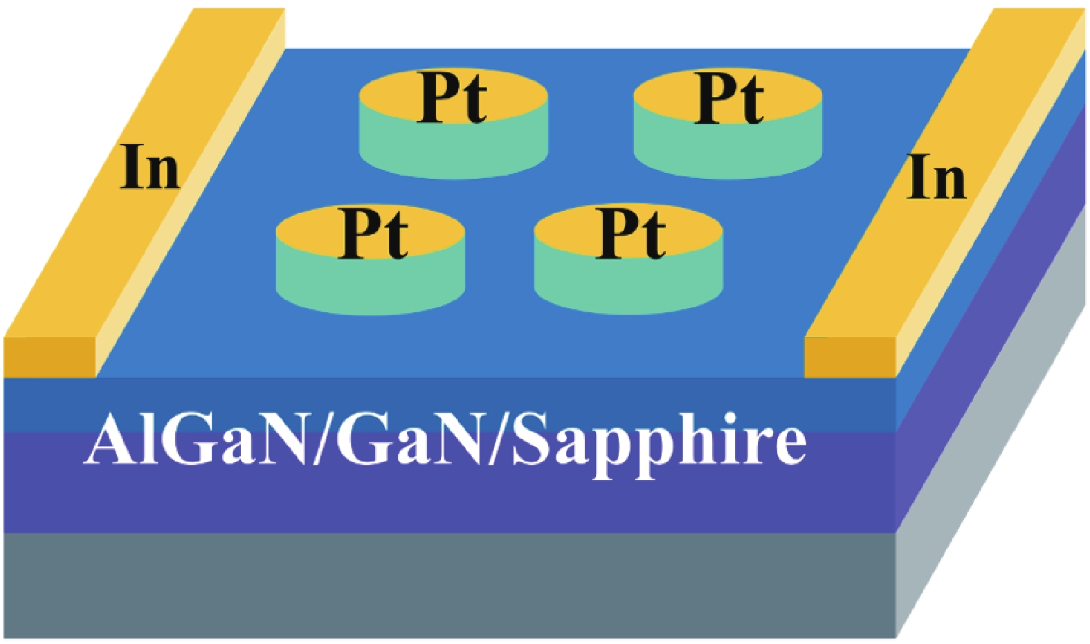
Fig. 1.
(Color online) Schematic of the Pt-AlGaN/GaN SBD under experimentation.
ARTICLES
Ashish Kumar1, 2, , Jayjit Mukherjee3, D. S. Rawal3, K. Asokan2 and D. Kanjilal2
Corresponding author: Ashish Kumar, ashish.kumar@ddn.upes.ac.in, dr.akmr@gmail.com
Abstract: Trap characterization on GaN Schottky barrier diodes (SBDs) has been carried out using deep-level transient spectroscopy (DLTS). Selective probing by varying the ratio of the rate window values (r) incites different trap signatures at similar temperature regimes. Electron traps are found to be within the values: 0.05–1.2 eV from the conduction band edge whereas the hole traps 1.37–2.66 eV from the valence band edge on the SBDs. In the lower temperature regime, the deeper electron traps contribute to the capacitance transients with increasing r values, whereas at the higher temperatures >300 K, a slow variation of the trap levels (both electrons and holes) is observed when r is varied. These traps are found to be mainly contributed to dislocations, interfaces, and vacancies within the structure.
Key words: deep traps, Pt-SBD, DLTS, rate window, defects
| [1] |
Mishra U K, Parikh P, Wu Y F. AlGaN/GaN HEMTs-an overview of device operation and applications. Proc IEEE, 2002, 90, 1022 doi: 10.1109/JPROC.2002.1021567
|
| [2] |
Millán J, Godignon P, Perpiñà X, et al. A survey of wide bandgap power semiconductor devices. IEEE Trans Power Electron, 2014, 29, 2155 doi: 10.1109/TPEL.2013.2268900
|
| [3] |
Davis R F. III-V nitrides for electronic and optoelectronic applications. Proc IEEE, 1991, 79, 702 doi: 10.1109/5.90133
|
| [4] |
Yu H B, Memon M H, Wang D H, et al. AlGaN-based deep ultraviolet micro-LED emitting at 275 nm. Opt Lett, 2021, 46, 3271 doi: 10.1364/OL.431933
|
| [5] |
Yu H, Memon M H, Jia H, et al. A 10 x 10 deep ultraviolet light-emitting micro-LED array. J Semicond, 2022, 43, 062801 doi: 10.1088/1674-4926/43/6/062801
|
| [6] |
Wang D H, Wu W T, Fang S, et al. Observation of polarity-switchable photoconductivity in III-nitride/MoSx core-shell nanowires. Light Sci Appl, 2022, 11, 227 doi: 10.1038/s41377-022-00912-7
|
| [7] |
Asghar M, Muret P, Beaumont B, et al. Field dependent transformation of electron traps in GaN p-n diodes grown by metal-organic chemical vapour deposition. Mater Sci Eng B, 2004, 113, 248 doi: 10.1016/j.mseb.2004.09.001
|
| [8] |
Moroz V, Wong H Y, Choi M, et al. The impact of defects on GaN device behavior: Modeling dislocations, traps, and pits. ECS J Solid State Sci Technol, 2016, 5, P3142 doi: 10.1149/2.0211604jss
|
| [9] |
Usami S, Ando Y, Tanaka A, et al. Correlation between dislocations and leakage current of p-n diodes on a free-standing GaN substrate. Appl Phys Lett, 2018, 112, 182106 doi: 10.1063/1.5024704
|
| [10] |
Saito W, Kuraguchi M, Takada Y, et al. Influence of surface defect charge at AlGaN-GaN-HEMT upon Schottky gate leakage current and breakdown voltage. IEEE Trans Electron Devices, 2005, 52, 159 doi: 10.1109/TED.2004.842710
|
| [11] |
Ghosh S, Das S, Dinara S M, et al. Off-state leakage and current collapse in AlGaN/GaN HEMTs: a virtual gate induced by dislocations. IEEE Trans Electron Devices, 2018, 65, 1333 doi: 10.1109/TED.2018.2808334
|
| [12] |
Lee I H, Polyakov A Y, Smirnov N B, et al. Changes in electron and hole traps in GaN-based light emitting diodes from near-UV to green spectral ranges. Appl Phys Lett, 2017, 110, 192107 doi: 10.1063/1.4983556
|
| [13] |
Shiojima K, Suemitsu T, Ogura M. Correlation between current-voltage characteristics and dislocations for n-GaN Schottky contacts. Appl Phys Lett, 2001, 78, 3636 doi: 10.1063/1.1370538
|
| [14] |
Saito W, Takada Y, Kuraguchi M, et al. Recessed-gate structure approach toward normally off high-Voltage AlGaN/GaN HEMT for power electronics applications. IEEE Trans Electron Devices, 2006, 53, 356 doi: 10.1109/TED.2005.862708
|
| [15] |
Saadat O I, Chung J W, Piner E L, et al. Gate-first AlGaN/GaN HEMT technology for high-frequency applications. IEEE Electron Device Lett, 2009, 30, 1254 doi: 10.1109/LED.2009.2032938
|
| [16] |
Lee F, Su L Y, Wang C H, et al. Impact of gate metal on the performance of p-GaN/AlGaN/GaN high electron mobility transistors. IEEE Electron Device Lett, 2015, 36, 232 doi: 10.1109/LED.2015.2395454
|
| [17] |
Kumar A, Mahajan S, Vinayak S. Studies on the thermal stability of Ni/n-GaN and Pt/n-GaN Schottky barrier diodes. Mater Res Express, 2016, 3, 085901 doi: 10.1088/2053-1591/3/8/085901
|
| [18] |
Huang Y P, Hsu W C, Liu H Y, et al. Enhancement-mode tri-gate nanowire InAlN/GaN MOSHEMT for power applications. IEEE Electron Device Lett, 2019, 40, 929 doi: 10.1109/LED.2019.2911698
|
| [19] |
Lide D R. CRC handbook of chemistry and physics. Boca Raton: CRC Press, 2001
|
| [20] |
Wang L, Nathan M I, Lim T H, et al. High barrier height GaN Schottky diodes: Pt/GaN and Pd/GaN. Appl Phys Lett, 1996, 68, 1267 doi: 10.1063/1.115948
|
| [21] |
Jeon C M, Lee J L. Enhancement of Schottky barrier height on AlGaN/GaN heterostructure by oxidation annealing. Appl Phys Lett, 2003, 82, 4301 doi: 10.1063/1.1583140
|
| [22] |
Wang J, Zhao D, Sun Y, et al. Thermal annealing behaviour of Pt on n-GaN schottky contacts. J Appl Phys, 2003, 36, 1018 doi: 10.1088/0022-3727/36/8/312
|
| [23] |
Kumar S, Gupta P, Guiney I, et al. Temperature and bias dependent trap capture cross section in AlGaN/GaN HEMT on 6-in silicon with carbon-doped buffer. IEEE Trans Electron Devices, 2017, 64, 4868 doi: 10.1109/TED.2017.2757516
|
| [24] |
Kumar A, Kumar M, Kaur R, et al. Barrier height enhancement of Ni/GaN Schottky diode using Ru based passivation scheme. Appl Phys Lett, 2014, 104, 133510 doi: 10.1063/1.4870624
|
| [25] |
Kumar A, Singh T, Kumar M, et al. Sulphide passivation of GaN based schottky diodes. Curr Appl Phys, 2014, 14, 491 doi: 10.1016/j.cap.2013.12.021
|
| [26] |
Lang D V. Deep-level transient spectroscopy: A new method to characterize traps in semiconductors. J Appl Phys, 1974, 45, 3023 doi: 10.1063/1.1663719
|
| [27] |
Reshchikov M A, Morkoç H, Park S S, et al. Transient photoluminescence of defect transitions in freestanding GaN. Appl Phys Lett, 2001, 78, 2882 doi: 10.1063/1.1370119
|
| [28] |
Bouya M, Malbert N, Labat N, et al. Analysis of traps effect on AlGaN/GaN HEMT by luminescence techniques. Microelectron Reliab, 2008, 48, 1366 doi: 10.1016/j.microrel.2008.07.052
|
| [29] |
Reshchikov M, Shahedipour F, Korotkov R, et al. Deep acceptors in undoped GaN. Phys B, 1999, 273, 105 doi: 10.1016/S0921-4526(99)00417-2
|
| [30] |
Reshchikov M A, Morkoç H. Luminescence properties of defects in GaN. J Appl Phys, 2005, 97, 061301 doi: 10.1063/1.1868059
|
| [31] |
Belahsene S, Al Saqri N A, Jameel D, et al. Analysis of deep level defects in GaN pin diodes after beta particle irradiation. Electronics, 2015, 4, 1090 doi: 10.3390/electronics4041090
|
| [32] |
Venturi G, Castaldini A, Cavallini A, et al. Dislocation-related trap levels in nitride-based light emitting diodes. Appl Phys Lett, 2014, 104, 211102 doi: 10.1063/1.4879644
|
| [33] |
Jones R, Elsner J, Haugk M, et al. Interaction of oxygen with threading dislocations in GaN. Phys Status Solidi A, 1999, 171, 167 doi: 10.1002/(SICI)1521-396X(199901)171:1<167::AIDPSSA167>3.0.CO;2-M
|
| [34] |
Fang Z Q, Look D C, Kim D H, et al. Traps in AlGaN/GaN/SiC heterostructures studied by deep level transient spectroscopy. Appl Phys Lett, 2005, 87, 182115 doi: 10.1063/1.2126145
|
| [35] |
Fang Z Q, Claflin B, Look D C, et al. Deep traps in AlGaN/GaN heterostructures studied by deep level transient spectroscopy: Effect of carbon concentration in GaN buffer layers. J Appl Phys, 2010, 108, 063706 doi: 10.1063/1.3488610
|
| [36] |
Polyakov A Y, Lee I H. Deep traps in GaN-based structures as affecting the performance of GaN devices. Mater Sci Eng R, 2015, 94, 1 doi: 10.1016/j.mser.2015.05.001
|
| [37] |
Boguslawski P, Briggs E L, Bernholc J. Native defects in gallium nitride. Phys Rev B, 1995, 51, 17255 doi: 10.1103/PhysRevB.51.17255
|
| [38] |
Umana-Membreno G A, Dell J M, Hessler T P, et al. 60Co gamma-irradiation-induced defects in n-GaN. Appl Phys Lett, 2002, 80, 4354 doi: 10.1063/1.1483390
|
| [39] |
Kumar A, Kanjilal D, Kumar V, et al. Defect formation in GaN epitaxial layers due to swift heavy ion irradiation. Radiation Effects and Defects in Solids, 2011, 166, 739 doi: 10.1080/10420150.2011.569716
|
| [40] |
Kumar A, Dhillon J, Verma S, et al. Identification of swift heavy ion induced defects in Pt/n-GaN Schottky diodes by in-situ deep level transient spectroscopy. Semicond Sci Technol, 2018, 33, 085008 doi: 10.1088/1361-6641/aacd54
|
| [41] |
Polenta L, Fang Z Q, Look D C. On the main irradiation-induced defect in GaN. Appl Phys Lett, 2000, 76, 2086 doi: 10.1063/1.126263
|
| [42] |
Look D C, Reynolds D, Hemsky J W, et al. Defect donor and acceptor in GaN. Phys Rev Lett, 1997, 79, 2273 doi: 10.1103/PhysRevLett.79.2273
|
| [43] |
Fang Z Q, Farlow G C, Claflin B, et al. Effects of electron-irradiation on electrical properties of AlGaN/GaN Schottky barrier diodes. J Appl Phys, 2009, 105, 123704 doi: 10.1063/1.3151952
|
| [44] |
Das A, Ko D H, Lin R M, et al. Anomalous decrease of off-state drain leakage current in GaN/AlGaN HEMTs with dual optical excitation. IEEE Electron Device Lett, 2014, 35, 820 doi: 10.1109/LED.2014.2327647
|
| [45] |
Mizutani T, Kawano A, Kishimoto S, et al. Drain current DLTS of normally-off AlGaN/GaN HEMTs. Phys Status Solidi C, 2007, 4, 1536 doi: 10.1002/pssc.200674155
|
| [46] |
Polyakov A Y, Smirnov N, Govorkov A, et al. Deep centers and persistent photocapacitance in AlGaN/GaN high electron mobility transistor structures grown on Si substrates. J Vac Sci Technol B, 2013, 31, 011211 doi: 10.1116/1.4773057
|
| [47] |
Armstrong A, Crawford M H, Koleske D D. Quantitative and depth-resolved investigation of deep-level defects in InGaN/GaN heterostructures. J Electron Mater, 2011, 40, 369 doi: 10.1007/s11664-010-1453-4
|
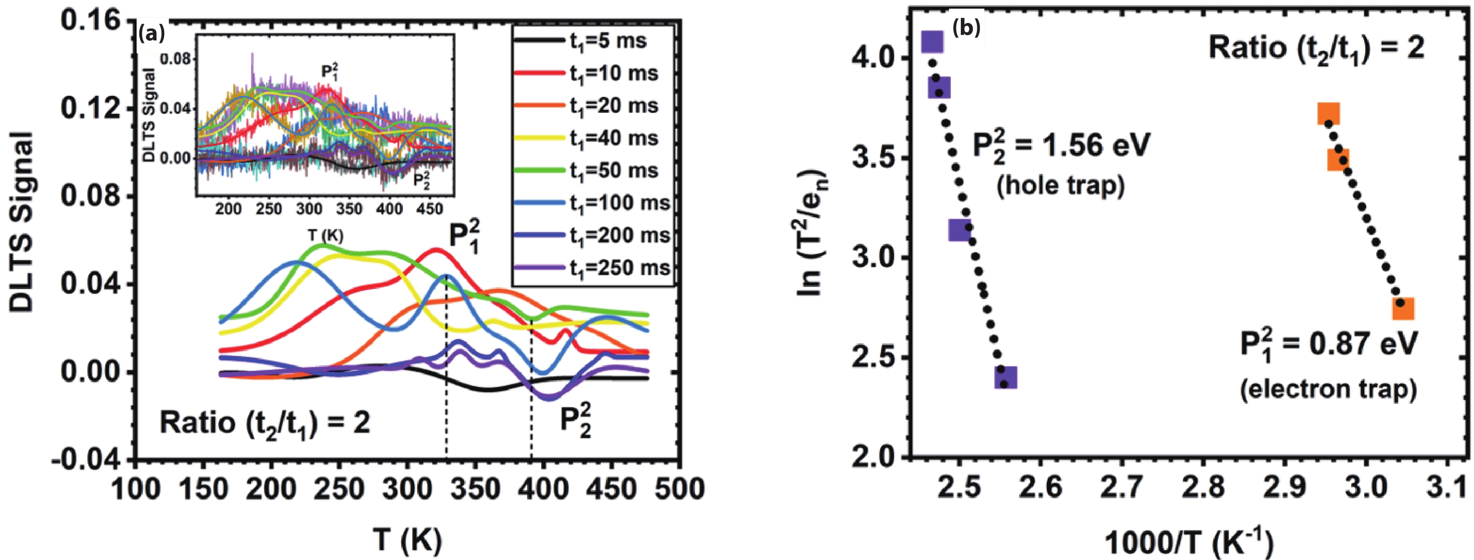
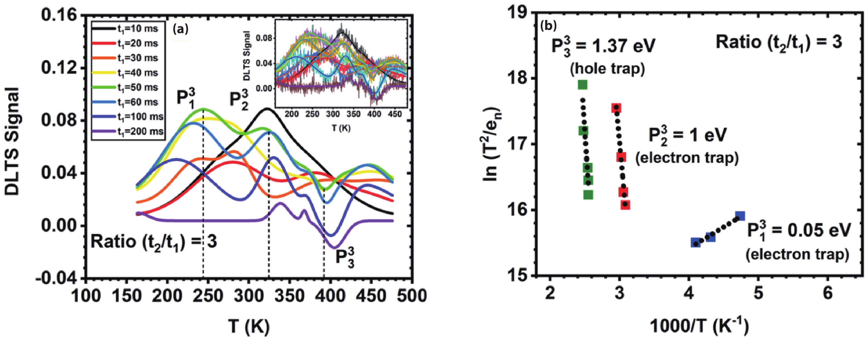
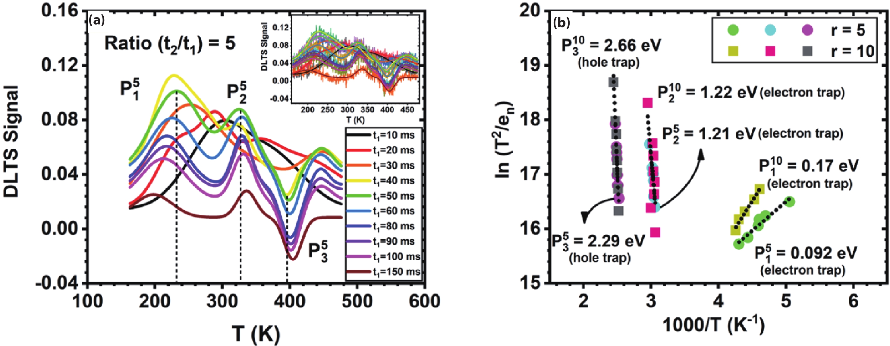
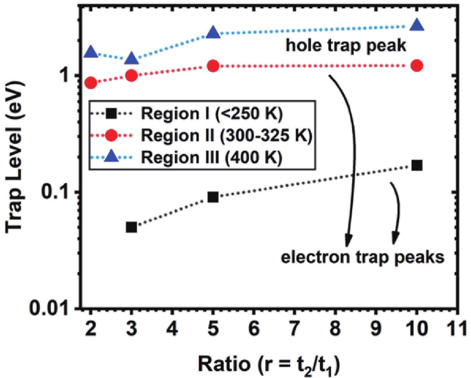
Table 1. Summary of the electron and hole traps from the DLTS experimentation. Ea is the activation energy of the trap measured from the conduction (EC) or valence band (wV) edge, and NT is the trap density as calculated from the Arrhenius plots.
| Ratio (r) | Trap peak, nature | Ea (eV) | NT (1016 cm−3) | Remark | Ref. |
| 2 | $ {P}_{1}^{2} $, e | EC – 0.87 | 2.05 | Nitrogen interstitial (Ni) | [29–31] |
| $ {P}_{2}^{2} $, h | EV + 1.56 | 1.03 | |||
| 3 | $ {P}_{1}^{3} $, e | EC – 0.05 | 5.14 | Open core dislocation | [32, 35] |
| $ {P}_{2}^{3} $, e | EC – 1.00 | 3.08 | Threading dislocations | [34] | |
| $ {P}_{3}^{3} $, h | EV + 1.37 | 1.17 | AlGaN/GaN interface | [35,36] | |
| 5 | $ {P}_{1}^{5} $, e | EC – 0.09 | 4.41 | Nitrogen vacancies | [37, 38, 41]* |
| $ {P}_{2}^{5} $, e | EC – 1.21 | 3.23 | Extended defects in GaN | [35, 36] | |
| $ {P}_{3}^{5} $, h | EV + 2.29 | 1.54 | Ga-vacancy/N-antisite | [44] | |
| 10 | $ {P}_{1}^{10} $, e | EC – 0.17 | 2.82 | Bulk GaN/interface states | [45, 46] |
| $ {P}_{2}^{10} $, e | EC – 1.22 | 2.79 | Extended defects in GaN | [35, 36] | |
| $ {P}_{3}^{10} $, h | EV + 2.66 | 1.45 | Point/extended defects | [47] | |
| *This trap level was also evident after e/$ \gamma $-irradiation on GaN SBDs. | |||||
 DownLoad: CSV
| [1] |
Mishra U K, Parikh P, Wu Y F. AlGaN/GaN HEMTs-an overview of device operation and applications. Proc IEEE, 2002, 90, 1022 doi: 10.1109/JPROC.2002.1021567
|
| [2] |
Millán J, Godignon P, Perpiñà X, et al. A survey of wide bandgap power semiconductor devices. IEEE Trans Power Electron, 2014, 29, 2155 doi: 10.1109/TPEL.2013.2268900
|
| [3] |
Davis R F. III-V nitrides for electronic and optoelectronic applications. Proc IEEE, 1991, 79, 702 doi: 10.1109/5.90133
|
| [4] |
Yu H B, Memon M H, Wang D H, et al. AlGaN-based deep ultraviolet micro-LED emitting at 275 nm. Opt Lett, 2021, 46, 3271 doi: 10.1364/OL.431933
|
| [5] |
Yu H, Memon M H, Jia H, et al. A 10 x 10 deep ultraviolet light-emitting micro-LED array. J Semicond, 2022, 43, 062801 doi: 10.1088/1674-4926/43/6/062801
|
| [6] |
Wang D H, Wu W T, Fang S, et al. Observation of polarity-switchable photoconductivity in III-nitride/MoSx core-shell nanowires. Light Sci Appl, 2022, 11, 227 doi: 10.1038/s41377-022-00912-7
|
| [7] |
Asghar M, Muret P, Beaumont B, et al. Field dependent transformation of electron traps in GaN p-n diodes grown by metal-organic chemical vapour deposition. Mater Sci Eng B, 2004, 113, 248 doi: 10.1016/j.mseb.2004.09.001
|
| [8] |
Moroz V, Wong H Y, Choi M, et al. The impact of defects on GaN device behavior: Modeling dislocations, traps, and pits. ECS J Solid State Sci Technol, 2016, 5, P3142 doi: 10.1149/2.0211604jss
|
| [9] |
Usami S, Ando Y, Tanaka A, et al. Correlation between dislocations and leakage current of p-n diodes on a free-standing GaN substrate. Appl Phys Lett, 2018, 112, 182106 doi: 10.1063/1.5024704
|
| [10] |
Saito W, Kuraguchi M, Takada Y, et al. Influence of surface defect charge at AlGaN-GaN-HEMT upon Schottky gate leakage current and breakdown voltage. IEEE Trans Electron Devices, 2005, 52, 159 doi: 10.1109/TED.2004.842710
|
| [11] |
Ghosh S, Das S, Dinara S M, et al. Off-state leakage and current collapse in AlGaN/GaN HEMTs: a virtual gate induced by dislocations. IEEE Trans Electron Devices, 2018, 65, 1333 doi: 10.1109/TED.2018.2808334
|
| [12] |
Lee I H, Polyakov A Y, Smirnov N B, et al. Changes in electron and hole traps in GaN-based light emitting diodes from near-UV to green spectral ranges. Appl Phys Lett, 2017, 110, 192107 doi: 10.1063/1.4983556
|
| [13] |
Shiojima K, Suemitsu T, Ogura M. Correlation between current-voltage characteristics and dislocations for n-GaN Schottky contacts. Appl Phys Lett, 2001, 78, 3636 doi: 10.1063/1.1370538
|
| [14] |
Saito W, Takada Y, Kuraguchi M, et al. Recessed-gate structure approach toward normally off high-Voltage AlGaN/GaN HEMT for power electronics applications. IEEE Trans Electron Devices, 2006, 53, 356 doi: 10.1109/TED.2005.862708
|
| [15] |
Saadat O I, Chung J W, Piner E L, et al. Gate-first AlGaN/GaN HEMT technology for high-frequency applications. IEEE Electron Device Lett, 2009, 30, 1254 doi: 10.1109/LED.2009.2032938
|
| [16] |
Lee F, Su L Y, Wang C H, et al. Impact of gate metal on the performance of p-GaN/AlGaN/GaN high electron mobility transistors. IEEE Electron Device Lett, 2015, 36, 232 doi: 10.1109/LED.2015.2395454
|
| [17] |
Kumar A, Mahajan S, Vinayak S. Studies on the thermal stability of Ni/n-GaN and Pt/n-GaN Schottky barrier diodes. Mater Res Express, 2016, 3, 085901 doi: 10.1088/2053-1591/3/8/085901
|
| [18] |
Huang Y P, Hsu W C, Liu H Y, et al. Enhancement-mode tri-gate nanowire InAlN/GaN MOSHEMT for power applications. IEEE Electron Device Lett, 2019, 40, 929 doi: 10.1109/LED.2019.2911698
|
| [19] |
Lide D R. CRC handbook of chemistry and physics. Boca Raton: CRC Press, 2001
|
| [20] |
Wang L, Nathan M I, Lim T H, et al. High barrier height GaN Schottky diodes: Pt/GaN and Pd/GaN. Appl Phys Lett, 1996, 68, 1267 doi: 10.1063/1.115948
|
| [21] |
Jeon C M, Lee J L. Enhancement of Schottky barrier height on AlGaN/GaN heterostructure by oxidation annealing. Appl Phys Lett, 2003, 82, 4301 doi: 10.1063/1.1583140
|
| [22] |
Wang J, Zhao D, Sun Y, et al. Thermal annealing behaviour of Pt on n-GaN schottky contacts. J Appl Phys, 2003, 36, 1018 doi: 10.1088/0022-3727/36/8/312
|
| [23] |
Kumar S, Gupta P, Guiney I, et al. Temperature and bias dependent trap capture cross section in AlGaN/GaN HEMT on 6-in silicon with carbon-doped buffer. IEEE Trans Electron Devices, 2017, 64, 4868 doi: 10.1109/TED.2017.2757516
|
| [24] |
Kumar A, Kumar M, Kaur R, et al. Barrier height enhancement of Ni/GaN Schottky diode using Ru based passivation scheme. Appl Phys Lett, 2014, 104, 133510 doi: 10.1063/1.4870624
|
| [25] |
Kumar A, Singh T, Kumar M, et al. Sulphide passivation of GaN based schottky diodes. Curr Appl Phys, 2014, 14, 491 doi: 10.1016/j.cap.2013.12.021
|
| [26] |
Lang D V. Deep-level transient spectroscopy: A new method to characterize traps in semiconductors. J Appl Phys, 1974, 45, 3023 doi: 10.1063/1.1663719
|
| [27] |
Reshchikov M A, Morkoç H, Park S S, et al. Transient photoluminescence of defect transitions in freestanding GaN. Appl Phys Lett, 2001, 78, 2882 doi: 10.1063/1.1370119
|
| [28] |
Bouya M, Malbert N, Labat N, et al. Analysis of traps effect on AlGaN/GaN HEMT by luminescence techniques. Microelectron Reliab, 2008, 48, 1366 doi: 10.1016/j.microrel.2008.07.052
|
| [29] |
Reshchikov M, Shahedipour F, Korotkov R, et al. Deep acceptors in undoped GaN. Phys B, 1999, 273, 105 doi: 10.1016/S0921-4526(99)00417-2
|
| [30] |
Reshchikov M A, Morkoç H. Luminescence properties of defects in GaN. J Appl Phys, 2005, 97, 061301 doi: 10.1063/1.1868059
|
| [31] |
Belahsene S, Al Saqri N A, Jameel D, et al. Analysis of deep level defects in GaN pin diodes after beta particle irradiation. Electronics, 2015, 4, 1090 doi: 10.3390/electronics4041090
|
| [32] |
Venturi G, Castaldini A, Cavallini A, et al. Dislocation-related trap levels in nitride-based light emitting diodes. Appl Phys Lett, 2014, 104, 211102 doi: 10.1063/1.4879644
|
| [33] |
Jones R, Elsner J, Haugk M, et al. Interaction of oxygen with threading dislocations in GaN. Phys Status Solidi A, 1999, 171, 167 doi: 10.1002/(SICI)1521-396X(199901)171:1<167::AIDPSSA167>3.0.CO;2-M
|
| [34] |
Fang Z Q, Look D C, Kim D H, et al. Traps in AlGaN/GaN/SiC heterostructures studied by deep level transient spectroscopy. Appl Phys Lett, 2005, 87, 182115 doi: 10.1063/1.2126145
|
| [35] |
Fang Z Q, Claflin B, Look D C, et al. Deep traps in AlGaN/GaN heterostructures studied by deep level transient spectroscopy: Effect of carbon concentration in GaN buffer layers. J Appl Phys, 2010, 108, 063706 doi: 10.1063/1.3488610
|
| [36] |
Polyakov A Y, Lee I H. Deep traps in GaN-based structures as affecting the performance of GaN devices. Mater Sci Eng R, 2015, 94, 1 doi: 10.1016/j.mser.2015.05.001
|
| [37] |
Boguslawski P, Briggs E L, Bernholc J. Native defects in gallium nitride. Phys Rev B, 1995, 51, 17255 doi: 10.1103/PhysRevB.51.17255
|
| [38] |
Umana-Membreno G A, Dell J M, Hessler T P, et al. 60Co gamma-irradiation-induced defects in n-GaN. Appl Phys Lett, 2002, 80, 4354 doi: 10.1063/1.1483390
|
| [39] |
Kumar A, Kanjilal D, Kumar V, et al. Defect formation in GaN epitaxial layers due to swift heavy ion irradiation. Radiation Effects and Defects in Solids, 2011, 166, 739 doi: 10.1080/10420150.2011.569716
|
| [40] |
Kumar A, Dhillon J, Verma S, et al. Identification of swift heavy ion induced defects in Pt/n-GaN Schottky diodes by in-situ deep level transient spectroscopy. Semicond Sci Technol, 2018, 33, 085008 doi: 10.1088/1361-6641/aacd54
|
| [41] |
Polenta L, Fang Z Q, Look D C. On the main irradiation-induced defect in GaN. Appl Phys Lett, 2000, 76, 2086 doi: 10.1063/1.126263
|
| [42] |
Look D C, Reynolds D, Hemsky J W, et al. Defect donor and acceptor in GaN. Phys Rev Lett, 1997, 79, 2273 doi: 10.1103/PhysRevLett.79.2273
|
| [43] |
Fang Z Q, Farlow G C, Claflin B, et al. Effects of electron-irradiation on electrical properties of AlGaN/GaN Schottky barrier diodes. J Appl Phys, 2009, 105, 123704 doi: 10.1063/1.3151952
|
| [44] |
Das A, Ko D H, Lin R M, et al. Anomalous decrease of off-state drain leakage current in GaN/AlGaN HEMTs with dual optical excitation. IEEE Electron Device Lett, 2014, 35, 820 doi: 10.1109/LED.2014.2327647
|
| [45] |
Mizutani T, Kawano A, Kishimoto S, et al. Drain current DLTS of normally-off AlGaN/GaN HEMTs. Phys Status Solidi C, 2007, 4, 1536 doi: 10.1002/pssc.200674155
|
| [46] |
Polyakov A Y, Smirnov N, Govorkov A, et al. Deep centers and persistent photocapacitance in AlGaN/GaN high electron mobility transistor structures grown on Si substrates. J Vac Sci Technol B, 2013, 31, 011211 doi: 10.1116/1.4773057
|
| [47] |
Armstrong A, Crawford M H, Koleske D D. Quantitative and depth-resolved investigation of deep-level defects in InGaN/GaN heterostructures. J Electron Mater, 2011, 40, 369 doi: 10.1007/s11664-010-1453-4
|


Article views: 898 Times PDF downloads: 99 Times Cited by: 0 Times
Received: 19 October 2022 Revised: 25 November 2022 Online: Accepted Manuscript: 13 January 2023Uncorrected proof: 14 January 2023Published: 10 April 2023
| Citation: |
Ashish Kumar, Jayjit Mukherjee, D. S. Rawal, K. Asokan, D. Kanjilal. Trap analysis on Pt-AlGaN/GaN Schottky barrier diode through deep level transient spectroscopy[J]. Journal of Semiconductors, 2023, 44(4): 042802. doi: 10.1088/1674-4926/44/4/042802
A Kumar, J Mukherjee, D S Rawal, K Asokan, D Kanjilal. Trap analysis on Pt-AlGaN/GaN Schottky barrier diode through deep level transient spectroscopy[J]. J. Semicond, 2023, 44(4): 042802. doi: 10.1088/1674-4926/44/4/042802
Export: BibTex EndNote

|
| [1] |
Mishra U K, Parikh P, Wu Y F. AlGaN/GaN HEMTs-an overview of device operation and applications. Proc IEEE, 2002, 90, 1022 doi: 10.1109/JPROC.2002.1021567
|
| [2] |
Millán J, Godignon P, Perpiñà X, et al. A survey of wide bandgap power semiconductor devices. IEEE Trans Power Electron, 2014, 29, 2155 doi: 10.1109/TPEL.2013.2268900
|
| [3] |
Davis R F. III-V nitrides for electronic and optoelectronic applications. Proc IEEE, 1991, 79, 702 doi: 10.1109/5.90133
|
| [4] |
Yu H B, Memon M H, Wang D H, et al. AlGaN-based deep ultraviolet micro-LED emitting at 275 nm. Opt Lett, 2021, 46, 3271 doi: 10.1364/OL.431933
|
| [5] |
Yu H, Memon M H, Jia H, et al. A 10 x 10 deep ultraviolet light-emitting micro-LED array. J Semicond, 2022, 43, 062801 doi: 10.1088/1674-4926/43/6/062801
|
| [6] |
Wang D H, Wu W T, Fang S, et al. Observation of polarity-switchable photoconductivity in III-nitride/MoSx core-shell nanowires. Light Sci Appl, 2022, 11, 227 doi: 10.1038/s41377-022-00912-7
|
| [7] |
Asghar M, Muret P, Beaumont B, et al. Field dependent transformation of electron traps in GaN p-n diodes grown by metal-organic chemical vapour deposition. Mater Sci Eng B, 2004, 113, 248 doi: 10.1016/j.mseb.2004.09.001
|
| [8] |
Moroz V, Wong H Y, Choi M, et al. The impact of defects on GaN device behavior: Modeling dislocations, traps, and pits. ECS J Solid State Sci Technol, 2016, 5, P3142 doi: 10.1149/2.0211604jss
|
| [9] |
Usami S, Ando Y, Tanaka A, et al. Correlation between dislocations and leakage current of p-n diodes on a free-standing GaN substrate. Appl Phys Lett, 2018, 112, 182106 doi: 10.1063/1.5024704
|
| [10] |
Saito W, Kuraguchi M, Takada Y, et al. Influence of surface defect charge at AlGaN-GaN-HEMT upon Schottky gate leakage current and breakdown voltage. IEEE Trans Electron Devices, 2005, 52, 159 doi: 10.1109/TED.2004.842710
|
| [11] |
Ghosh S, Das S, Dinara S M, et al. Off-state leakage and current collapse in AlGaN/GaN HEMTs: a virtual gate induced by dislocations. IEEE Trans Electron Devices, 2018, 65, 1333 doi: 10.1109/TED.2018.2808334
|
| [12] |
Lee I H, Polyakov A Y, Smirnov N B, et al. Changes in electron and hole traps in GaN-based light emitting diodes from near-UV to green spectral ranges. Appl Phys Lett, 2017, 110, 192107 doi: 10.1063/1.4983556
|
| [13] |
Shiojima K, Suemitsu T, Ogura M. Correlation between current-voltage characteristics and dislocations for n-GaN Schottky contacts. Appl Phys Lett, 2001, 78, 3636 doi: 10.1063/1.1370538
|
| [14] |
Saito W, Takada Y, Kuraguchi M, et al. Recessed-gate structure approach toward normally off high-Voltage AlGaN/GaN HEMT for power electronics applications. IEEE Trans Electron Devices, 2006, 53, 356 doi: 10.1109/TED.2005.862708
|
| [15] |
Saadat O I, Chung J W, Piner E L, et al. Gate-first AlGaN/GaN HEMT technology for high-frequency applications. IEEE Electron Device Lett, 2009, 30, 1254 doi: 10.1109/LED.2009.2032938
|
| [16] |
Lee F, Su L Y, Wang C H, et al. Impact of gate metal on the performance of p-GaN/AlGaN/GaN high electron mobility transistors. IEEE Electron Device Lett, 2015, 36, 232 doi: 10.1109/LED.2015.2395454
|
| [17] |
Kumar A, Mahajan S, Vinayak S. Studies on the thermal stability of Ni/n-GaN and Pt/n-GaN Schottky barrier diodes. Mater Res Express, 2016, 3, 085901 doi: 10.1088/2053-1591/3/8/085901
|
| [18] |
Huang Y P, Hsu W C, Liu H Y, et al. Enhancement-mode tri-gate nanowire InAlN/GaN MOSHEMT for power applications. IEEE Electron Device Lett, 2019, 40, 929 doi: 10.1109/LED.2019.2911698
|
| [19] |
Lide D R. CRC handbook of chemistry and physics. Boca Raton: CRC Press, 2001
|
| [20] |
Wang L, Nathan M I, Lim T H, et al. High barrier height GaN Schottky diodes: Pt/GaN and Pd/GaN. Appl Phys Lett, 1996, 68, 1267 doi: 10.1063/1.115948
|
| [21] |
Jeon C M, Lee J L. Enhancement of Schottky barrier height on AlGaN/GaN heterostructure by oxidation annealing. Appl Phys Lett, 2003, 82, 4301 doi: 10.1063/1.1583140
|
| [22] |
Wang J, Zhao D, Sun Y, et al. Thermal annealing behaviour of Pt on n-GaN schottky contacts. J Appl Phys, 2003, 36, 1018 doi: 10.1088/0022-3727/36/8/312
|
| [23] |
Kumar S, Gupta P, Guiney I, et al. Temperature and bias dependent trap capture cross section in AlGaN/GaN HEMT on 6-in silicon with carbon-doped buffer. IEEE Trans Electron Devices, 2017, 64, 4868 doi: 10.1109/TED.2017.2757516
|
| [24] |
Kumar A, Kumar M, Kaur R, et al. Barrier height enhancement of Ni/GaN Schottky diode using Ru based passivation scheme. Appl Phys Lett, 2014, 104, 133510 doi: 10.1063/1.4870624
|
| [25] |
Kumar A, Singh T, Kumar M, et al. Sulphide passivation of GaN based schottky diodes. Curr Appl Phys, 2014, 14, 491 doi: 10.1016/j.cap.2013.12.021
|
| [26] |
Lang D V. Deep-level transient spectroscopy: A new method to characterize traps in semiconductors. J Appl Phys, 1974, 45, 3023 doi: 10.1063/1.1663719
|
| [27] |
Reshchikov M A, Morkoç H, Park S S, et al. Transient photoluminescence of defect transitions in freestanding GaN. Appl Phys Lett, 2001, 78, 2882 doi: 10.1063/1.1370119
|
| [28] |
Bouya M, Malbert N, Labat N, et al. Analysis of traps effect on AlGaN/GaN HEMT by luminescence techniques. Microelectron Reliab, 2008, 48, 1366 doi: 10.1016/j.microrel.2008.07.052
|
| [29] |
Reshchikov M, Shahedipour F, Korotkov R, et al. Deep acceptors in undoped GaN. Phys B, 1999, 273, 105 doi: 10.1016/S0921-4526(99)00417-2
|
| [30] |
Reshchikov M A, Morkoç H. Luminescence properties of defects in GaN. J Appl Phys, 2005, 97, 061301 doi: 10.1063/1.1868059
|
| [31] |
Belahsene S, Al Saqri N A, Jameel D, et al. Analysis of deep level defects in GaN pin diodes after beta particle irradiation. Electronics, 2015, 4, 1090 doi: 10.3390/electronics4041090
|
| [32] |
Venturi G, Castaldini A, Cavallini A, et al. Dislocation-related trap levels in nitride-based light emitting diodes. Appl Phys Lett, 2014, 104, 211102 doi: 10.1063/1.4879644
|
| [33] |
Jones R, Elsner J, Haugk M, et al. Interaction of oxygen with threading dislocations in GaN. Phys Status Solidi A, 1999, 171, 167 doi: 10.1002/(SICI)1521-396X(199901)171:1<167::AIDPSSA167>3.0.CO;2-M
|
| [34] |
Fang Z Q, Look D C, Kim D H, et al. Traps in AlGaN/GaN/SiC heterostructures studied by deep level transient spectroscopy. Appl Phys Lett, 2005, 87, 182115 doi: 10.1063/1.2126145
|
| [35] |
Fang Z Q, Claflin B, Look D C, et al. Deep traps in AlGaN/GaN heterostructures studied by deep level transient spectroscopy: Effect of carbon concentration in GaN buffer layers. J Appl Phys, 2010, 108, 063706 doi: 10.1063/1.3488610
|
| [36] |
Polyakov A Y, Lee I H. Deep traps in GaN-based structures as affecting the performance of GaN devices. Mater Sci Eng R, 2015, 94, 1 doi: 10.1016/j.mser.2015.05.001
|
| [37] |
Boguslawski P, Briggs E L, Bernholc J. Native defects in gallium nitride. Phys Rev B, 1995, 51, 17255 doi: 10.1103/PhysRevB.51.17255
|
| [38] |
Umana-Membreno G A, Dell J M, Hessler T P, et al. 60Co gamma-irradiation-induced defects in n-GaN. Appl Phys Lett, 2002, 80, 4354 doi: 10.1063/1.1483390
|
| [39] |
Kumar A, Kanjilal D, Kumar V, et al. Defect formation in GaN epitaxial layers due to swift heavy ion irradiation. Radiation Effects and Defects in Solids, 2011, 166, 739 doi: 10.1080/10420150.2011.569716
|
| [40] |
Kumar A, Dhillon J, Verma S, et al. Identification of swift heavy ion induced defects in Pt/n-GaN Schottky diodes by in-situ deep level transient spectroscopy. Semicond Sci Technol, 2018, 33, 085008 doi: 10.1088/1361-6641/aacd54
|
| [41] |
Polenta L, Fang Z Q, Look D C. On the main irradiation-induced defect in GaN. Appl Phys Lett, 2000, 76, 2086 doi: 10.1063/1.126263
|
| [42] |
Look D C, Reynolds D, Hemsky J W, et al. Defect donor and acceptor in GaN. Phys Rev Lett, 1997, 79, 2273 doi: 10.1103/PhysRevLett.79.2273
|
| [43] |
Fang Z Q, Farlow G C, Claflin B, et al. Effects of electron-irradiation on electrical properties of AlGaN/GaN Schottky barrier diodes. J Appl Phys, 2009, 105, 123704 doi: 10.1063/1.3151952
|
| [44] |
Das A, Ko D H, Lin R M, et al. Anomalous decrease of off-state drain leakage current in GaN/AlGaN HEMTs with dual optical excitation. IEEE Electron Device Lett, 2014, 35, 820 doi: 10.1109/LED.2014.2327647
|
| [45] |
Mizutani T, Kawano A, Kishimoto S, et al. Drain current DLTS of normally-off AlGaN/GaN HEMTs. Phys Status Solidi C, 2007, 4, 1536 doi: 10.1002/pssc.200674155
|
| [46] |
Polyakov A Y, Smirnov N, Govorkov A, et al. Deep centers and persistent photocapacitance in AlGaN/GaN high electron mobility transistor structures grown on Si substrates. J Vac Sci Technol B, 2013, 31, 011211 doi: 10.1116/1.4773057
|
| [47] |
Armstrong A, Crawford M H, Koleske D D. Quantitative and depth-resolved investigation of deep-level defects in InGaN/GaN heterostructures. J Electron Mater, 2011, 40, 369 doi: 10.1007/s11664-010-1453-4
|

 WeChat ID
Journal of Semiconductors © 2017 All Rights Reserved 京ICP备05085259号-2