


1. Introduction
H and He ions implanted into semiconductor materials are widely used in the microelectronics industry. The implanted H and He ions are used in the ion cutting process to transfer the film from the implanted substrate layer to another handle material[1-4]. This technology is developed by Bruel and is called the “smart-cut”[1]. Smart-cut technology was first used by Soitec in France to fabricate silicon on insulator (SOI) wafers for sale on the market. Therefore, the mechanism of ion implantation induced fracture of Si materials has been studied relatively thoroughly[5-10]. The damage caused by H ion in the lattice is primarily vacancy and interstitial defects. The defects produced by He ion implantation into the lattice are actually excessive vacancies, which are mainly related to the role of He atoms. At room temperature, these vacancies and interstitial defects can recombine in the subsequent implantation process until stable complexes are formed[11]. During the annealing process, these complexes are transformed and precipitated in the form of nano-sized platelet defects. The platelet defects are further increased through Ostwald ripening mechanism and finally coalesced to form micro-size cracks parallel to the wafer surface[12, 13]. If the implantation depth is not too deep, the surface can elastically relax the stress imposed by the gas pressure in the cavity, which can cause the surface to blisters. If the surface cannot release the stress due to its excessive amplitude or the cavity is too deep below the surface, the cracks can propagate parallel to the surface and are finally exfoliated from the top, leaving craters on the surface[14]. This is called layer exfoliation. Blisters formation and material exfoliation are considered as the prerequisites for successful material ion cutting.
For the study of GaAs crystal exfoliation, extensive and deep research has also been carried out. Radu et al.[15] compared the exfoliation of the GaAs surface in the case of only implanted He ions and co-implanted H and He ions. They observed that in the process of He ion implantation, nano-sized He bubbles were generated in the damaged layer. These bubbles had high pressure and they were used as a reservoir for the diffusion of He during the annealing process after ion implantation. Gawlik et al.[16] demonstrated the effect of target temperature distribution on blister formation by two-step H ion implantation. They found that the mobility of H ions implanted at high temperature is strong, which may lead to the formation of nanoscale complexes. The H ions implanted at low temperature were more evenly distributed in the target lattice. Giguere et al.[17] implanted different fluences of H, D and He into GaAs (100) wafers and the fluence varied from 1016 to 1017 cm–2. The samples were rapidly annealed at 400 °C for 30 s. They finally concluded that GaAs implanted with low-energy H and D ions had an isotope effect and a narrow implantation fluence window, which led to surface exfoliation and blisters. Woo et al.[18] studied the dynamic behavior of blistering and spalling of the GaAs (100) surface implanted with H and He. They found that the ion beam cutting process of the GaAs layer transfer was very sensitive to both H implantation temperature and fluence. For the implantation fluence of 1.0 to 2.0 × 10¹⁷ H+/cm2, the optimal implantation temperature range is 120–160 °C. In addition, the optimal annealing temperature for GaAs layer transfer is in the range of 225–275 °C. Sun et al. [19] found that the co-implantation of He and H ions is more efficient in exfoliating the GaAs thin film with a lower thermal budget and lower density of defects in comparison with the case of the single He/H ion implantation.
Blistering, spalling and splitting are frequently observed in ions implanted into semiconductor surfaces[20-22]. In order to find the optimal ion implantation fluence, improve the surface exfoliation efficiency and reduce the required cost, we have studied the potential mechanism of implantation fluence dependence and blistering under different ion combinations. The influence of H, He ion implantation on the atomic mechanism of blistering observed after annealing has been studied in detail. Then, we discuss the change of blistering efficiency and explain the phenomena of blistering precursors and their physical interactions. Finally, the relationship between damage distribution and annealing temperature is studied.
2. Experimental methods
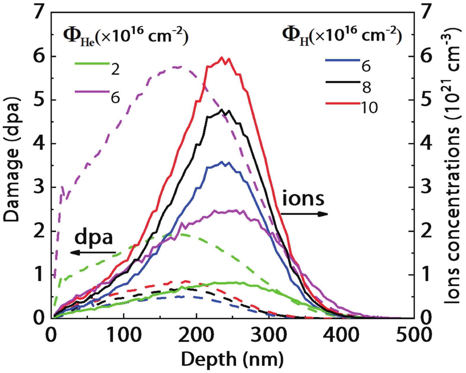
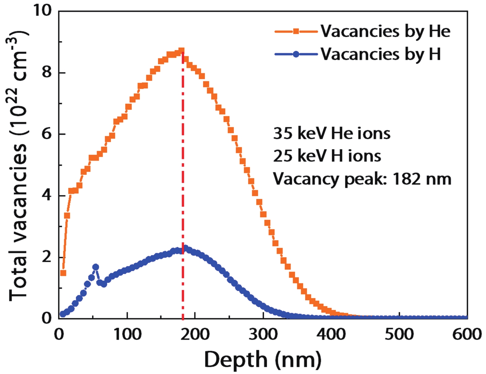
GaAs (100) substrates are successively implanted with He and H ions at room temperature. The implantation energy of He and H ions is 35 and 25 keV, respectively. In order to explore the interaction mechanism of GaAs crystal with implanted He and H ions, we have conducted implantation experiments with different fluence combinations. The fluence of He ion is 2 × 10¹⁶ and 6 × 1016 cm–2 and the fluence of H ion ranges from 2 × 10¹⁶ to 1 × 1017 cm–2, as shown in Table 1. In order to avoid the implantation channel effect, the direction of the ion beam is tilted 7° relative to the normal direction perpendicular to the sample surface. According to the stopping and range of ions in matter (SRIM) calculation[23], the distribution of implanted ion concentration and damage is shown in Fig. 1. The peak concentration of He ion is 240 nm from the surface and the peak damage depth is 180 nm from the surface. The peak concentration distribution of H ion coincides with that of He ion. The peak damage of H ion coincides with that of He ion and the peak damage is between 0.3 and 0.6 dpa. The peak damage distribution of H and He ions is shallower than their peak concentration distribution.
| Sample | Material | He+ fluence (1016 cm–2) | H+ fluence (1016 cm–2) | He+ energy (keV) | H+ energy (keV) |
| a | GaAs | 6 | — | 35 | — |
| b | GaAs | 2 | 6 | 35 | 25 |
| c | GaAs | — | 8 | — | 25 |
| d | GaAs | — | 10 | — | 25 |
 DownLoad:
CSV
| Show Table
DownLoad:
CSV
| Show Table

After implantation, the samples are cut into 10 × 10 mm2 squares. These squares are placed in the annealing furnace and annealed at 150, 200, and 250 °C under N2 atmosphere for 1 h. Raman spectroscopy (Renishaw, Britain) is used to study the change of GaAs surface stress before and after implantation and after annealing. The 532 nm laser is used as a light source and the output power of the laser is maintained between 50–200 mW. The surface stress of GaAs is characterized by the shift of Raman spectrum. The gas-filled blisters on the sample surface are imaged with an Olympus optical microscope (OM). Atomic force microscopy (AFM) is used to quantitatively study the three-dimensional morphology of blisters, such as diameter and height[24]. Cross-sectional transmission electron microscopy (XTEM) is used to selectively detect the defect microstructures (bubbles and nano/microcracks) in GaAs crystals. Before XTEM analysis, the samples are thinned by focused ion beam (FIB) to meet the needs of observation. XTEM images are taken at 200 keV using a JEOL 2100F field emission TEM.
3. Results and discussion
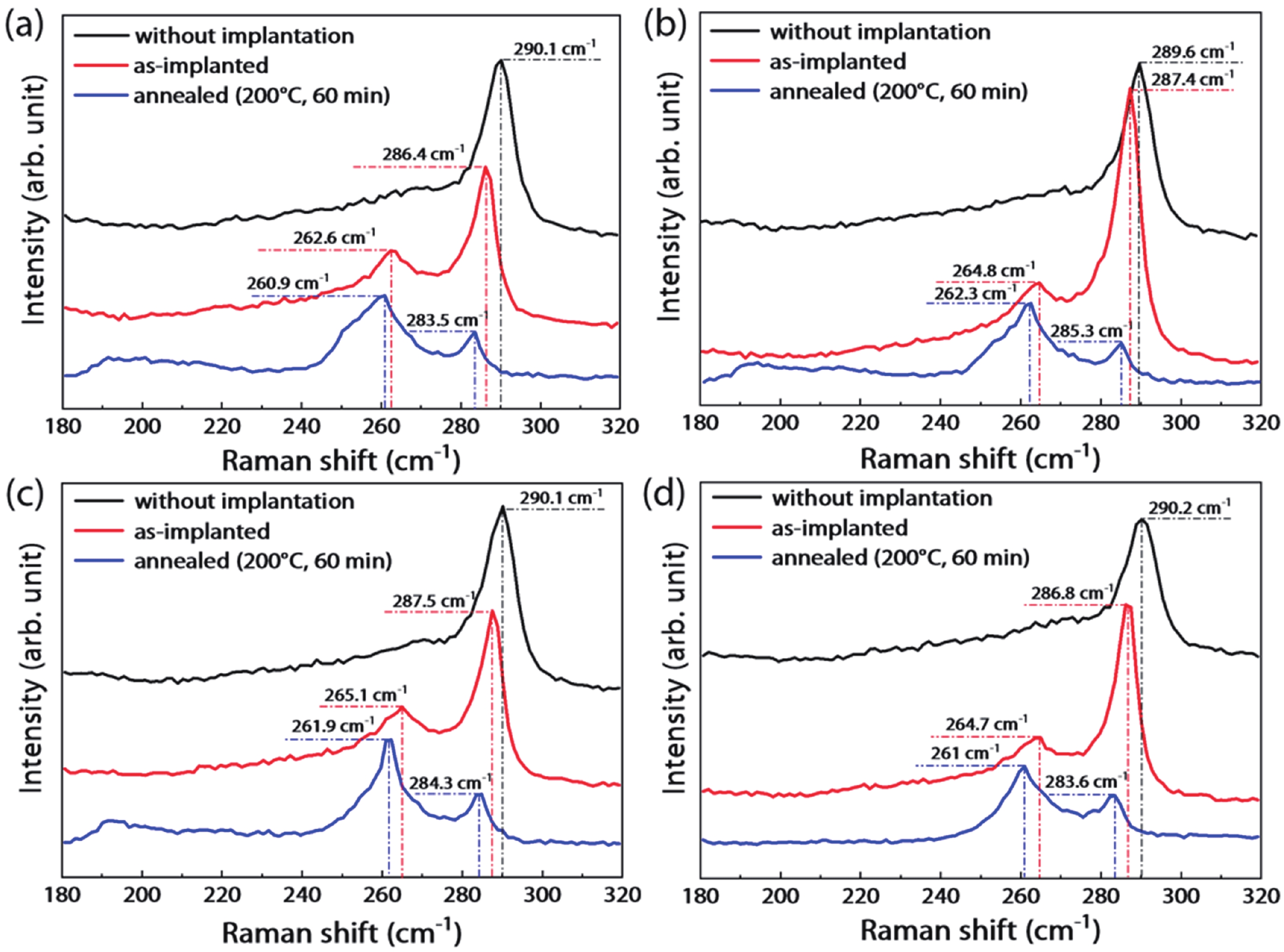
Raman spectroscopy is usually used as a non-destructive method to measure the stress on the surface of crystalline coatings with crystalline or amorphous structures. The ability of stress measurement is based on the relative frequency shift of Raman spectrum when lattice strain occurs. In principle, according to the selection rules of symmetric Raman dispersion tensor analysis, for (100) oriented zinc blende structure GaAs, longitudinal optical (LO) phonons can appear in the Raman spectrum of backscattering geometry, while transverse optical (TO) phonons are generally symmetrically forbidden[25, 26]. However, in the process of ion implantation, many factors, such as strain or defect, can be introduced into the GaAs lattice, resulting in the momentum non-conservation in the system, which can relax the Raman scattering selection rules, making the prohibited TO-GaAs mode appear. Therefore, the existence of surface defects is helpful to break the Raman scattering selection rule. For GaAs crystals without ion implantation, LO phonons are located near 289.7 cm−1 and TO phonons are located near 269 cm−1[27-29]. As shown in Figs. 2(a)–2(d), the black curves represent the Raman spectrum of GaAs without ion implantation. At the same time, no TO-GaAs mode peak is observed. After ion implantation, the surface of GaAs substrate is characterized by Raman spectrum again. The red curves represent the Raman spectrum after implantation. It can be seen that the Raman peak of the TO-GaAs mode appears at this time. With the increase of the total fluence, not only the weak TO phonon peak begins to appear, but also the peak position shows a certain blue shift at a larger fluence. The He atom is made up of two protons, twice as much as H. In the process of ion implantation, the effect of one He atom is about that of two H atoms. The weak TO phonon peak and strong LO phonon peak are located near 265 and 287 cm−1, respectively. Then, the implanted GaAs crystals are annealed and after annealing, four groups of samples are tested again by Raman spectroscopy. The blue curves represent the Raman peak after annealing. It can be seen that the intensity of the TO phonon peak after annealing is greater than that of the LO phonon peak. As a whole, there is a certain blue shift in the peak position compared with the non-annealed GaAs crystal. The frequency shift of the Raman spectrum is very sensitive to the stress on the sample. Generally, when there is a compressive stress in the sample, the bond length of the molecule decreases, the force constant increases, the vibration frequency increases, and the Raman spectrum can shift to the right; in contrast, when there is tensile stress in the sample, the Raman spectrum shifts to the left and the wave number decreases. The subsequent analysis shows that the slight frequency shift is mainly caused by the tensile stress caused by the annealed surface of ion implanted GaAs crystal. It can be seen from Fig. 2 that the Raman spectra of the four groups of samples have a certain frequency shift after annealing. When the annealing temperature gradually increases, the surface stress increases first and then decreases due to stress relief. The shift of the LO peak and the TO peak of sample a are 6.6 and 1.7 cm−1 respectively. The shift of the LO peak and the TO peak of sample b are 4.3 and 2.5 cm−1 respectively. The shift of the LO peak and the TO peak of sample c are 5.8 and 3.2 cm−1 respectively. The shift of the LO peak and the TO peak of sample d are 6.6 and 3.7 cm−1 respectively. As far as the shift of LO peak is concerned, sample a and sample d are the largest. At this time, the tensile stress on the GaAs surface is the largest. The shift of the LO peak of sample b and sample c is small, and the corresponding tensile stress on the GaAs surface is relatively small.

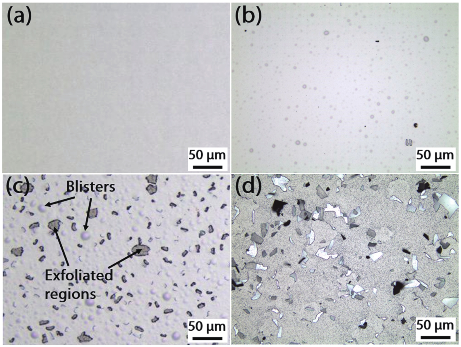
Four groups of implanted samples are placed in the annealing furnace. Nitrogen is filled in the chamber as the protective gas. The four groups of samples are annealed at 150, 200, and 250 °C for 1 h respectively, and the surface morphology changes show consistent results. Here, sample b is selected to display the results. As shown in Fig. 3(a), no blisters or craters are observed on the surface before annealing. When sample b is annealed at 150 °C for 1 h, blisters appear on the surface, as shown in Fig. 3(b). This shows that the blistering threshold of the GaAs surface is near 150 °C. When the annealing temperature is further increased to 200 °C, the surface of the sample appears to exfoliate. The shapes of craters and blisters are round, as shown in Fig. 3(c). Finally, when the annealing temperature is further increased to 250 °C and annealed at this temperature for 1 h, a large area of exfoliation occurs on the surface and the blisters disappear, as shown in Fig. 3(d). Fig. 3 shows the change of surface exfoliation morphology at different annealing temperatures. With the increase of annealing temperature, the density of surface blisters first increases and then decreases and the size of exfoliation gradually increases. In addition, the size and density of blisters and craters also depend significantly on the implantation fluence. With the increase of implantation fluence, the density of blisters and craters on the surface can increase even if the annealing temperature is appropriately lowered.

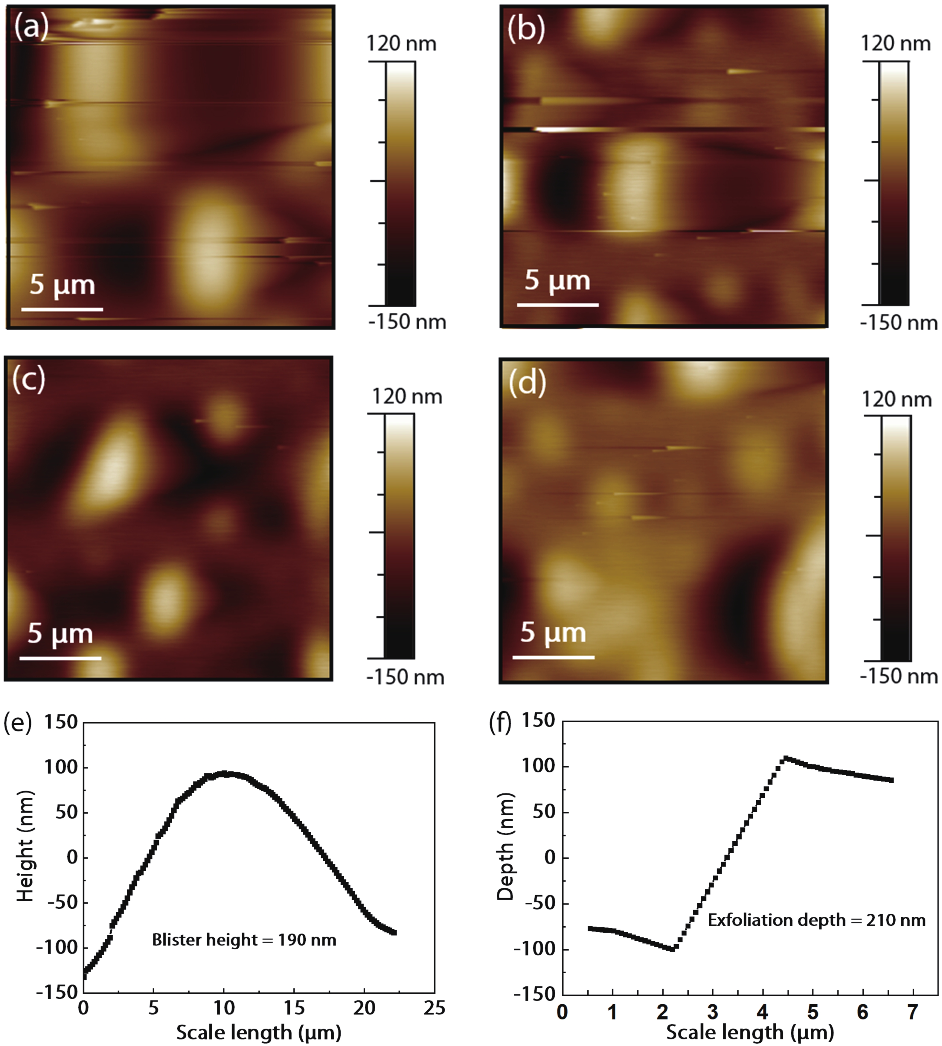
Fig. 4 shows the surface AFM images of four groups of GaAs (100) surfaces with different implantation fluences annealed at 200 °C for 1 h. During the measurement, we use the same scale for all samples. It can be seen from Figs. 4(a), 4(b) and 4(d) that the density of blisters on the surface of sample a, b and d is relatively high and the exfoliation is relatively serious. The blister density and exfoliation size are relatively small. The high internal pressure generated in the cavity buried in the GaAs matrix results in the deformation of the material surface and the formation of blisters. The blisters are round and light in color. The whiter the blister color, the higher the blister height. When the pressure inside the blisters is too high, the blisters may break, leaving craters on the surface. The size of the crater is related to the diameter of the blister. Fig. 4(e) shows the height of the blister on the surface of sample a. It can be seen that the height of the blister is about 190 nm. In addition, we measure the depth of the crater exfoliated from the sample surface. Fig. 4(f) shows the height difference of the side wall of the crater. It can be seen from the figure that the depth of the crater is about 210 nm. The depth of the crater is consistent with the position of the peak concentration of H and He ions. In addition, in the sample a implanted with He ions only, we can find that the surface exfoliation is relatively severe. This shows that the main form of He ions is the generation of nano-sized He bubbles in the damaged layer. These nano-sized He bubbles are used as a reservoir for diffusion of He during annealing.

In the four groups of samples, sample b is co-implanted with H and He ions to realize the exfoliation of the GaAs surface. In order to study the action mechanism of H and He ions in GaAs materials, we select sample b as the research object. The study of sample b is helpful to reveal the mechanism of surface blistering and exfoliation of other three groups of single implantation samples. The ion implantation sequence of sample b is to implant He ion first and then H ion. We prepare the sample after ion implantation without annealing treatment by focused ion beam. After preparation, the sample is placed under TEM to observe the interface morphology. As shown in Fig. 5(a), there is a damaged layer with a thickness of about 150 nm at 100 nm from the sample surface. This damage layer is mainly composed of defects induced by He and H ion implantation. No nano-cracks are observed in the damage layer due to no annealing treatment. The lattice diffraction pattern in Fig. 5(a) can be obtained by lattice diffraction on the upper area of the damage layer, indicating that the single crystal is maintained above the damage layer. EDS is selected to detect the element components in the damage area. In Fig. 5(a), we select an area with a length of about 150 nm as the detection area. The element composition of the detection area is shown in Fig. 5(b). The elements in the damaged layer are mainly composed of Ga, As, O, Si and C. The presence of a small amount of oxygen element indicates that the sample is oxidized under natural conditions.

Both He and H ion implantation can produce a large number of vacancy-type defects in GaAs. It can be seen from Fig. 6(a) that the vacancy-type defects are mainly located at the end of the ion range. There is a damage band with a width of about 150 nm at the depth of 100 nm from the sample surface. These vacancy-type defects can form nanoscale bubbles in the material during subsequent annealing, as shown in Fig. 6(b). Because of the high permeability of He and H atoms in GaAs crystals, their migration and diffusion directly affects the evolution of defects after implantation and annealing. In the subsequent high-temperature annealing process, the bubbles further grow through the Ostwald ripening process and migration aggregation process[30, 31]. With the growth of bubbles, gas atoms can be released from the bubbles and escape through the sample surface, thus forming a stable cavity inside the sample, as shown in Fig. 6(c). Cavity formation is an important condition for surface exfoliation. Surface exfoliation requires not only a large pressure in the sample, but also a narrow crack or cavity layer. During the annealing process, gas atoms enter the crack or cavity layer and expand with the increase of annealing temperature. Due to the increase of pressure, the cracks further expand laterally, and the cavities are connected in a large area, leading to the GaAs surface exfoliation. For co-implantation of He and H ions, the first implanted He ions will produce a certain number of open volume defects to capture the subsequently implanted H ions in GaAs crystals. In the post annealing process, the open volume defects are first passivated by H ions to form a stable state. Then H atoms increases the internal pressure of open volume defects, which makes open volume defects grow into platelet defects due to the Ostwald ripening effect. Therefore, co-implantation of He and H ions can more effectively split the GaAs layers than implantation of He ions only, because fewer defects are introduced and the formation of platelet defects is more effective.

In the process of surface exfoliation or layer separation caused by bubble evolution, the roles and processes of the two gas atoms are different. H has active chemical properties and strong mobility. It participates in bond breaking, internal surface passivation, gas accumulation, pressure increase and fracture processes in GaAs materials[32]. He is an inert element, which plays a physical role in gas accumulation, pressure increase and fracture in GaAs materials. In the process of H ion implantation, GaAs dangling bonds can be passivated by combining with H atoms to form Ga–H–H–As bonds. This kind of bond energy is relatively weak, which leads to the formation of platelet defects after fracture, as shown in Fig. 6(c). In the subsequent thermal annealing process, H2 molecules aggregate to these platelet defects and these platelet defects increase continuously under the effect of internal pressure, thus forming nano-cracks, as shown in Figs. 6(d) and 6(e). With the further increase of annealing temperature, nano-cracks grow laterally and form continuous cracks in the sample, as shown in Fig. 6(f), which directly promotes the film exfoliation. Finally, we determine that the optimal ion implantation fluence for GaAs film transfer is 2 × 10¹⁶ and 6 × 10¹⁶ H+/cm2.
Based on Monte Carlo simulation, the distribution coincidence of vacancy-type defects generated by H and He ions in the GaAs crystal is calculated, as shown in Fig. 7. The vacancy-type defects can bind H atoms and stabilize H. Because the growth of bubbles mainly comes from the interaction between vacancy-type defects and gas atoms, additional vacancy-type defects and gas atoms in the H implantation layer can promote the growth of cavities. During thermal annealing, He atoms can be desorbed from He bubbles and diffuse to the sample surface. During the diffusion process, these He atoms can be captured by the H complex, further promoting the bubble growth and increasing the pressure in the bubble. Considering the above factors, compared with H or He ion single implantation, H and He ion co-implantation can improve the exfoliation efficiency of GaAs materials.

4. Conclusion
In conclusion, we have carried out four groups of ion implantation experiments on GaAs and realized the exfoliation of GaAs film with a thickness of about 210 nm. Compared with the implantation of H or He ions only, co-implantation of H and He ions at room temperature can achieve GaAs film exfoliation more effectively with lower thermal budget and lower defect density. The optimal ion implantation condition of 2 × 10¹⁶ and 6 × 10¹⁶ H+/cm2 for GaAs film transfer is determined to improve the exfoliation efficiency of the surface. The surface of GaAs is characterized by Raman spectroscopy. It is found that with the increase of annealing temperature, the surface stress increase first and then decreases due to stress relief. OM and AFM are used to characterize the changes of surface morphology at different annealing temperatures. The bubble density on the surface of the four groups of samples increases first and then decreases, and the size of the surface craters gradually increases. The formation of defects induced by ion implantation and the mechanism of film exfoliation are revealed by TEM. Our research opens up new possibilities for large area exfoliation of GaAs films, and paves the way for the heterointegration of GaAs film on silicon.
Acknowledgements
This work is financially supported by the National Nature Science Foundation of China (Grant No. 61673222) and Wuxi University Research Start-up Fund for Introduced Talents (Grant No. 2022r036).
 DownLoad:


 Rui Huang:received his Ph.D. degree at Beijing University of Technology. He is currently a lecturer in Wuxi University. His research mainly focuses on wafer bonding, smart-cut, semiconductor materials, additive manufacturing technologies and Silicon-based heterointegration
 DownLoad:


