


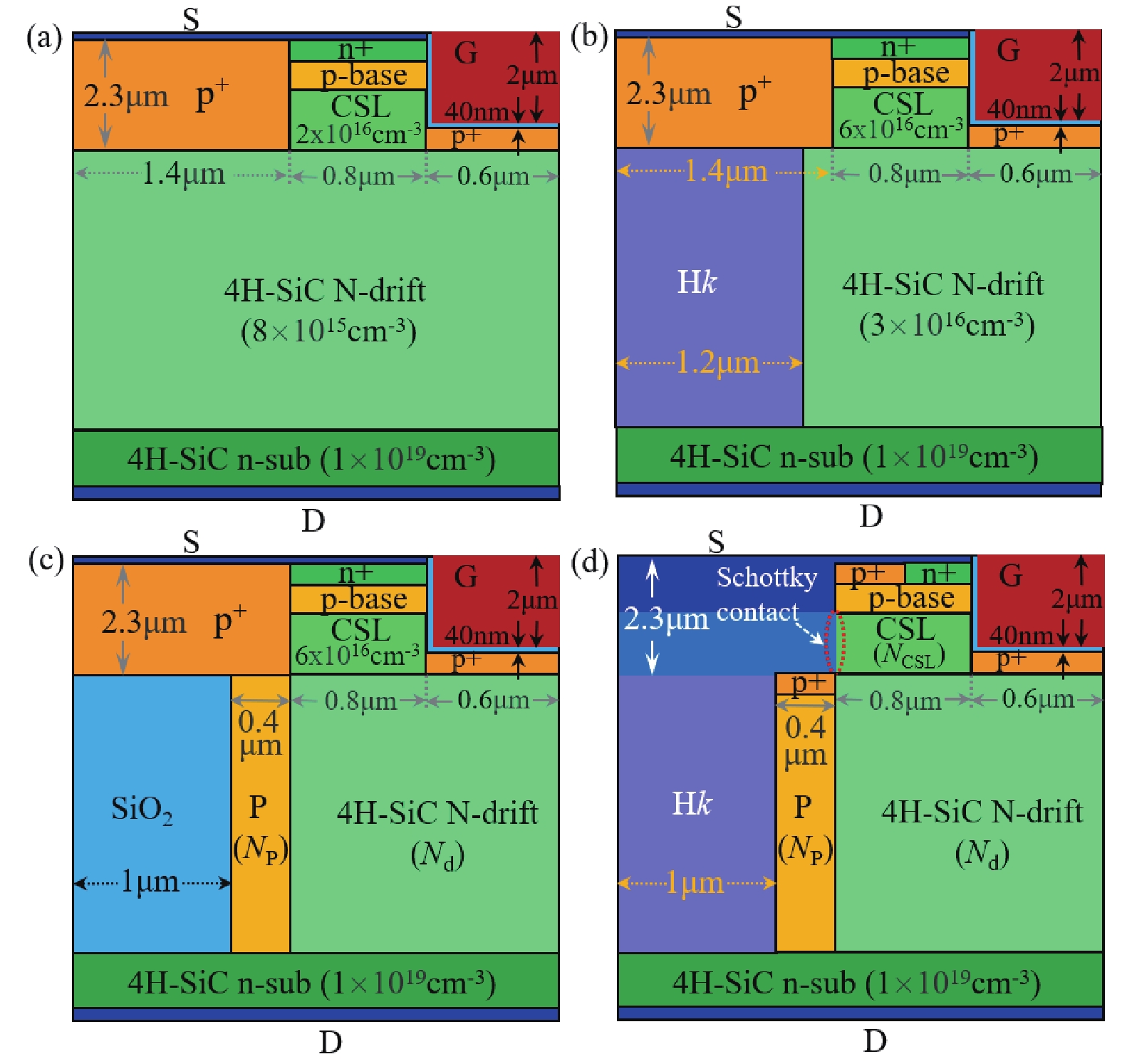
Fig. 1.
(Color online) (a) Conventional SiC MOSFET. (b) Hk SiC MOSFET. (c) SJ SiC MOSFET. (d) Proposed Hk-SJ-SBD SiC MOSFET.
ARTICLES
Moufu Kong1, , Zewei Hu1, Ronghe Yan1, Bo Yi1, Bingke Zhang2 and Hongqiang Yang1,
Corresponding author: Moufu Kong, kmf@uestc.edu.cn; Hongqiang Yang, hqyang@uestc.edu.cn
Abstract: A new SiC superjunction power MOSFET device using high-k insulator and p-type pillar with an integrated Schottky barrier diode (Hk-SJ-SBD MOSFET) is proposed, and has been compared with the SiC high-k MOSFET (Hk MOSFET), SiC superjuction MOSFET (SJ MOSFET) and the conventional SiC MOSFET in this article. In the proposed SiC Hk-SJ-SBD MOSFET, under the combined action of the p-type region and the Hk dielectric layer in the drift region, the concentration of the N-drift region and the current spreading layer can be increased to achieve an ultra-low specific on-resistance (Ron,sp). The integrated Schottky barrier diode (SBD) also greatly improves the reverse recovery performance of the device. TCAD simulation results indicate that the Ron,sp of the proposed SiC Hk-SJ-SBD MOSFET is 0.67 mΩ·cm2 with a 2240 V breakdown voltage (BV), which is more than 72.4%, 23%, 5.6% lower than that of the conventional SiC MOSFET, Hk SiC MOSFET and SJ SiC MOSFET with the 1950, 2220, and 2220 V BV, respectively. The reverse recovery time and reverse recovery charge of the proposed MOSFET is 16 ns and18 nC, which are greatly reduced by more than 74% and 94% in comparison with those of all the conventional SiC MOSFET, Hk SiC MOSFET and SJ SiC MOSFET, due to the integrated SBD in the proposed MOSFET. And the trade-off relationship between the Ron,sp and the BV is also significantly improved compared with that of the conventional MOSFET, Hk MOSFET and SJ MOSFET as well as the MOSFETs in other previous literature, respectively. In addition, compared with conventional SJ SiC MOSFET, the proposed SiC MOSFET has better immunity to charge imbalance, which may bring great application prospects.
Key words: SiC, MOSFET, specific on-resistance, breakdown voltage, high-k, superjunction, switching performance, reverse recovery characteristic
| [1] |
Oraon A, Shreya S, Kumari R, et al. A double trench 4H-SiC MOSFET as an enhanced model of SiC UMOSFET. 2017 7th International Symposium on Embedded Computing and System Design (ISED), 2018, 1 doi: 10.1109/ISED.2017.8303939
|
| [2] |
Yu H Y, Liang S W, Liu H Z, et al. Numerical study of SiC MOSFET with integrated n-/ n-type poly-Si/SiC heterojunction freewheeling diode. IEEE Trans Electron Devices, 2021, 68, 4571 doi: 10.1109/TED.2021.3097979
|
| [3] |
Huang H, Wang Y, Yu C H, et al. A high-performance SiC super-junction MOSFET with a step-doping profile. IEEE J Electron Devices Soc, 2021, 9, 1084 doi: 10.1109/JEDS.2021.3125706
|
| [4] |
Vudumula P, Kotamraju S. Design and optimization of 1.2-kV SiC planar inversion MOSFET using split dummy gate concept for high-frequency applications. IEEE Trans Electron Devices, 2019, 66, 5266 doi: 10.1109/TED.2019.2949459
|
| [5] |
Han K, Baliga B J, Sung W. Split-gate 1.2-kV 4H-SiC MOSFET: Analysis and experimental validation. IEEE Electron Device Lett, 2017, 38, 1437 doi: 10.1109/LED.2017.2738616
|
| [6] |
Kong M F, Hu Z W, Gao J C, et al. A 1200-V-class ultra-low specific on-resistance SiC lateral MOSFET with double trench gate and VLD technique. IEEE J Electron Devices Soc, 2021, 10, 83 doi: 10.1109/JEDS.2021.3136341
|
| [7] |
Liu Y T, Jin D H, Jiang S Q, et al. An active damping control method for the LLCL filter-based SiC MOSFET grid-connected inverter in vehicle-to-grid application. IEEE Trans Veh Technol, 2019, 68, 3411 doi: 10.1109/TVT.2019.2899166
|
| [8] |
Kim H, Chen H, Maksimović D, et al. SiC-MOSFET composite boost converter with 22 kW/L power density for electric vehicle application. 2017 IEEE Applied Power Electronics Conference and Exposition (APEC), 2017, 134 doi: 10.1109/APEC.2017.7930684
|
| [9] |
Anthon A, Zhang Z, Andersen M A E, et al. The benefits of SiC mosfets in a T-type inverter for grid-Tie applications. IEEE Trans Power Electron, 2016, 32, 2808 doi: 10.1109/TPEL.2016.2582344
|
| [10] |
Masuda T, Saito Y, Kumazawa T, et al. 0.63 mΩcm2 /1170V 4H H-SiC super junction V-groove trench MOSFET. 2018 IEEE International Electron Devices Meeting (IEDM), 2018, 484 doi: 10.1109/IEDM.2018.8614610
|
| [11] |
Baba M, Tawara T, Morimoto T, et al. Ultra-low specific on-resistance achieved in 3.3 kV-class SiC superjunction MOSFET. 2021 33rd International Symposium on Power Semiconductor Devices and ICs (ISPSD), 2021, 83 doi: 10.23919/ISPSD50666.2021.9452273
|
| [12] |
Ghandi R, Bolotnikov A, Kennerly S, et al. 4.5kV SiC charge-balanced MOSFETs with ultra-low on-resistance. 2020 32nd International Symposium on Power Semiconductor Devices and ICs (ISPSD), 2020, 126 doi: 10.1109/ISPSD46842.2020.9170171
|
| [13] |
Akshay K, Karmalkar S. Quick design of a superjunction considering charge imbalance due to process variations. IEEE Trans Electron Devices, 2020, 67, 3024 doi: 10.1109/TED.2020.2998443
|
| [14] |
Alam M, Morisette D T, Cooper J A. Design guidelines for superjunction devices in the presence of charge imbalance. IEEE Trans Electron Devices, 2018, 65, 3345 doi: 10.1109/TED.2018.2848584
|
| [15] |
Chen X B, Huang M M. A vertical power MOSFET with an interdigitated drift region using high-k insulator. IEEE Trans Electron Devices, 2012, 59, 2430 doi: 10.1109/TED.2012.2204890
|
| [16] |
Lyu X J, Chen X B. Vertical power Hk-MOSFET of hexagonal layout. IEEE Trans Electron Devices, 2013, 60, 1709 doi: 10.1109/TED.2013.2249068
|
| [17] |
Luo xiao rong, Cai jin yong, Fan Y, et al. Novel low-resistance current path UMOS with high-K dielectric Pillars. IEEE Trans Electron Devices, 2013, 60, 2840 doi: 10.1109/TED.2013.2272086
|
| [18] |
Naugarhiya A, Kondekar P N. High permittivity material selection for design of optimum Hk VDMOS. Superlattices Microstruct, 2015, 83, 310 doi: 10.1016/j.spmi.2015.02.045
|
| [19] |
He Z C, Cao M H, Wang N N, et al. Electron-pinned defect-dipoles for SrTiO3-based ceramics with high permittivity and low dielectric loss. 2016 Joint IEEE International Symposium on the Applications of Ferroelectrics, European Conference on Application of Polar Dielectrics, and Piezoelectric Force Microscopy Workshop (ISAF/ECAPD/PFM), 2016, 1 doi: https://doi.org/10.1109/ISAF.2016.7578071
|
| [20] |
Xia Z B, Chandrasekar H, Moore W, et al. Metal/BaTiO3/β-Ga2O3 dielectric heterojunction diode with 5.7 MV/cm breakdown field. Appl Phys Lett, 2019, 115, 252104 doi: 10.1063/1.5130669
|
| [21] |
Li J H, Li P, Huo W R, et al. Analysis and fabrication of an LDMOS with high-permittivity dielectric. IEEE Electron Device Lett, 2011, 32, 1266 doi: 10.1109/LED.2011.2158383
|
| [22] |
Yang H, Hu S D, Ran S L, et al. Simulative researching of a 1200V SiC trench MOSFET with an enhanced vertical RESURF effect. IEEE J Electron Devices Soc, 2020, 8, 1335 doi: 10.1109/JEDS.2020.3032649
|
| [23] |
Kitai H, Yamaguchi T, Hozumi Y, et al. A superior 15 kV SiC MOSFET with current spreading layer for high-frequency applications. Jpn J Appl Phys, 2019, 58, SBBD16 doi: 10.7567/1347-4065/ab01d1
|
| [24] |
Zheng Y L, Tang W M, Chau T, et al. Simulation study of 4H-SiC high-k pillar MOSFET with integrated Schottky barrier diode. IEEE J Electron Devices Soc, 2021, 9, 951 doi: 10.1109/JEDS.2021.3116715
|
| [25] |
Wang H Y, Wang C, Wang B Z, et al. 4H-SiC super-junction JFET: Design and experimental demonstration. IEEE Electron Device Lett, 2020, 41, 445 doi: 10.1109/LED.2020.2969683
|
| [26] |
Yano H, Nakao H, Mikami H, et al. Anomalously anisotropic channel mobility on trench sidewalls in 4H-SiC trench-gate metal-oxide-semiconductor field-effect transistors fabricated on 8° off substrates. Appl Phys Lett, 2007, 90, 042102 doi: 10.1063/1.2434157
|
| [27] |
Huang M M, Chen X B. A superjunction structure using high-kinsulator for power devices: Theory and optimization. J Semicond, 2016, 37, 064014 doi: 10.1088/1674-4926/37/6/064014
|
| [28] |
Zhao Y, Toyama M, Kita K, et al. Moisture-absorption-induced permittivity deterioration and surface roughness enhancement of lanthanum oxide films on silicon. Appl Phys Lett, 2006, 88, 072904 doi: 10.1063/1.2174840
|
| [29] |
Locquet J P, Marchiori C, Sousa M, et al. High-K dielectrics for the gate stack. J Appl Phys, 2006, 100, 051610 doi: 10.1063/1.2336996
|
| [30] |
Ji L F, Jiang Y J. Dielectric and microstructure modification of Ta2O5 ceramics by laser sintering. Mater Lett, 2006, 60, 86 doi: 10.1016/j.matlet.2005.07.077
|
| [31] |
Moon J H, Eom D I, No S Y, et al. Electrical properties of the La2O3/4H-SiC interface prepared by atomic layer deposition using La(iPrCp)3 and H2O. Mater Sci Forum, 2006, 527–529, 1083 doi: 10.4028/www.scientific.net/MSF.527-529.1083
|
| [32] |
Huang L H, Liu Y, Peng X, et al. Static performance and threshold voltage stability improvement of Al2O3/LaAlO3/SiO2 gate-stack for SiC power MOSFETs. IEEE Trans Electron Devices, 2022, 69, 690 doi: 10.1109/TED.2021.3138378
|
| [33] |
Yu J, Chen G, Li C X, et al. Hydrogen gas sensing properties of Pt/Ta2O5 Schottky diodes based on Si and SiC substrates. Sens Actuat A Phys, 2011, 172, 9 doi: 10.1016/j.sna.2011.02.021
|
| [34] |
Jinesh K B, Klootwijk J H, Lamy Y, et al. Enhanced electrical properties of atomic layer deposited La2O3 thin films with embedded ZrO2 nanocrystals. Appl Phys Lett, 2008, 93, 172904 doi: 10.1063/1.3009202
|
| [35] |
Kang S K, Ishiwara H. Characteristics of LaAlO3 as insulating buffer layers of ferroelectric-gate field effect transistors. Jpn J Appl Phys, 2002, 41, 6899 doi: 10.1143/JJAP.41.6899
|
| [36] |
Kao C H, Lai P L, Wang H Y. The comparison between Ta2O5 and Ti-doped Ta2O5 dielectrics. Surf Coat Technol, 2013, 231, 512 doi: 10.1016/j.surfcoat.2012.04.045
|
| [37] |
Agarwal A K, Seshadri S, Rowland L B. Temperature dependence of Fowler-Nordheim Current in 6H- and 4H-SiC MOS capacitors. IEEE Electron Device Lett, 1997, 18, 592 doi: 10.1109/55.644081
|
| [38] |
He Q Y, Luo X R, Liao T, et al. 4H-SiC superjunction trench MOSFET with reduced saturation current. Superlattices Microstruct, 2019, 125, 58 doi: 10.1016/j.spmi.2018.10.016
|
| [39] |
Wang Z G, Wang X, Kuo J B. Modeling power vertical high-k MOS device with interface charges via superposition methodology-breakdown voltage and specific ON-resistance. IEEE Trans Electron Devices, 2018, 65, 4947 doi: 10.1109/TED.2018.2870174
|
| [40] |
Noborio M, Jun S D, Kimoto T. P-channel MOSFETs on 4H-SiC {0001} and nonbasal faces fabricated by oxide deposition and N2O annealing. IEEE Trans Electron Devices, 2009, 56, 1953 doi: 10.1109/TED.2009.2025909
|
| [41] |
Pérez-Tomás A, Brosselard P, Hassan J, et al. Schottky versus bipolar 3.3 kV SiC diodes. Semicond Sci Technol, 2008, 23, 125004 doi: 10.1088/0268-1242/23/12/125004
|
| [42] |
Schilirò E, Lo Nigro R, Fiorenza P, et al. Negative charge trapping effects in Al2O3 films grown by atomic layer deposition onto thermally oxidized 4H-SiC. AIP Adv, 2016, 6, 075021 doi: 10.1063/1.4960213
|
| [43] |
Han S Y, Kim K H, Kim J K, et al. Ohmic contact formation mechanism of Ni on n-type 4H-SiC. Appl Phys Lett, 2001, 79, 1816 doi: 10.1063/1.1404998
|
| [44] |
Hatano M, Moon S, Lee M H, et al. In situ and ex situ diagnostics on melting and resolidification dynamics of amorphous and polycrystalline silicon thin films during excimer laser annealing. J Non Cryst Solids, 2000, 266–269, 654 doi: 10.1016/S0022-3093(99)00768-1
|
| [45] |
Pécz B. Contact formation in SiC devices. Appl Surf Sci, 2001, 184, 287 doi: 10.1016/S0169-4332(01)00678-X
|
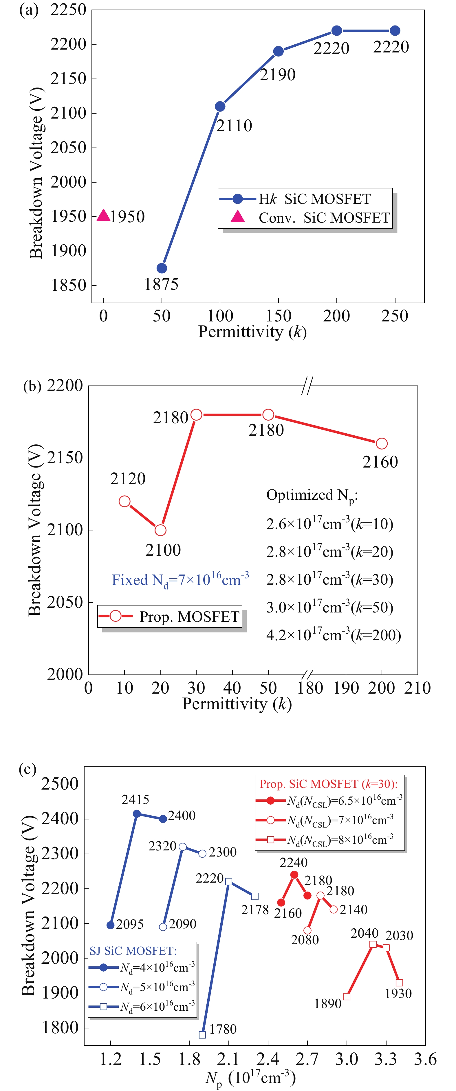
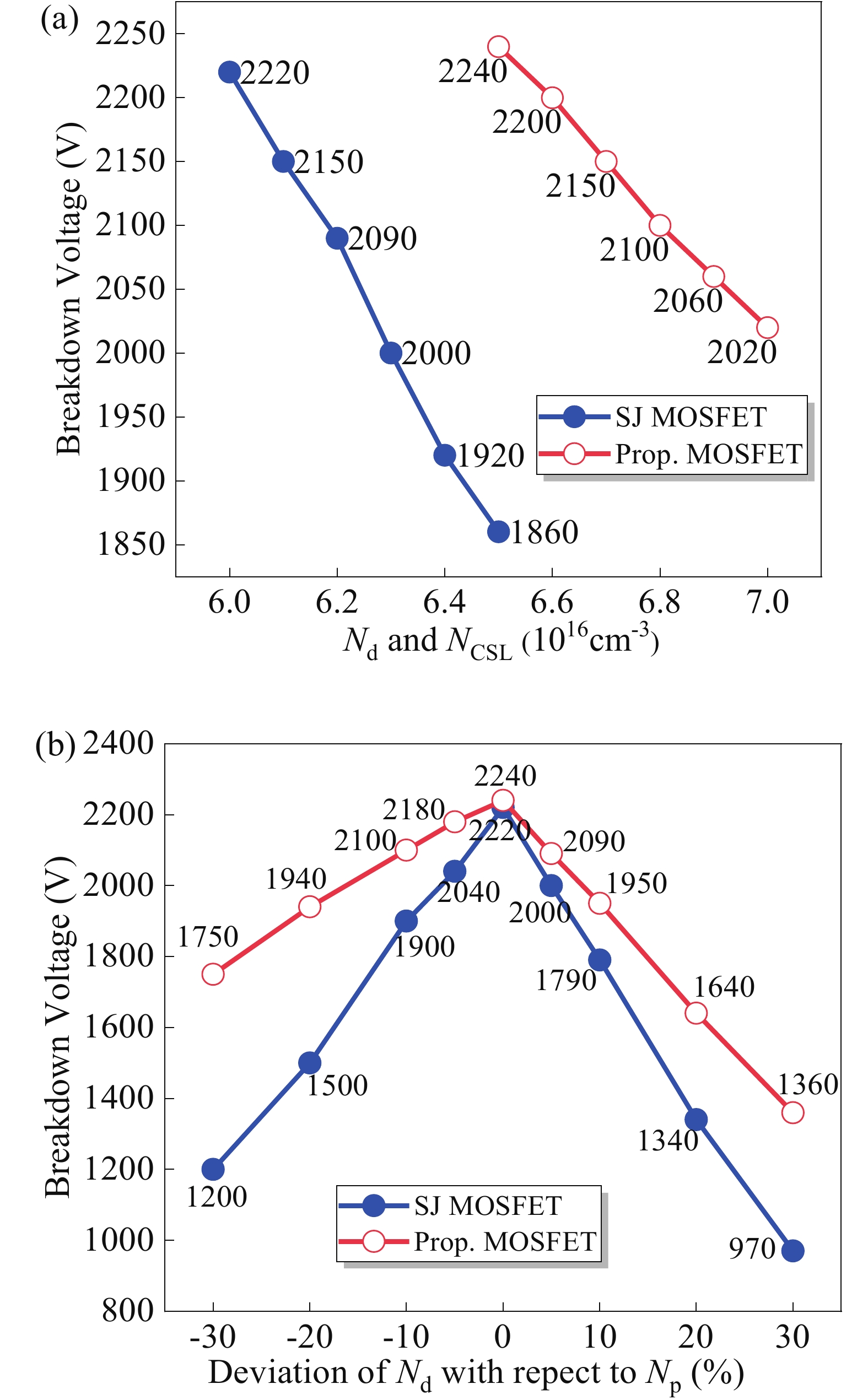
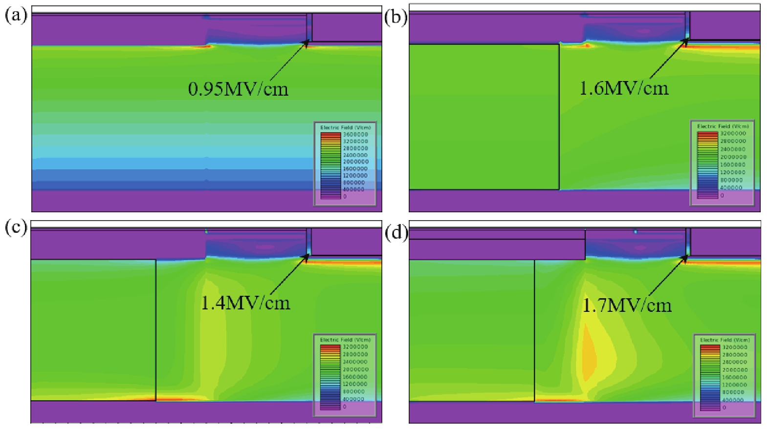
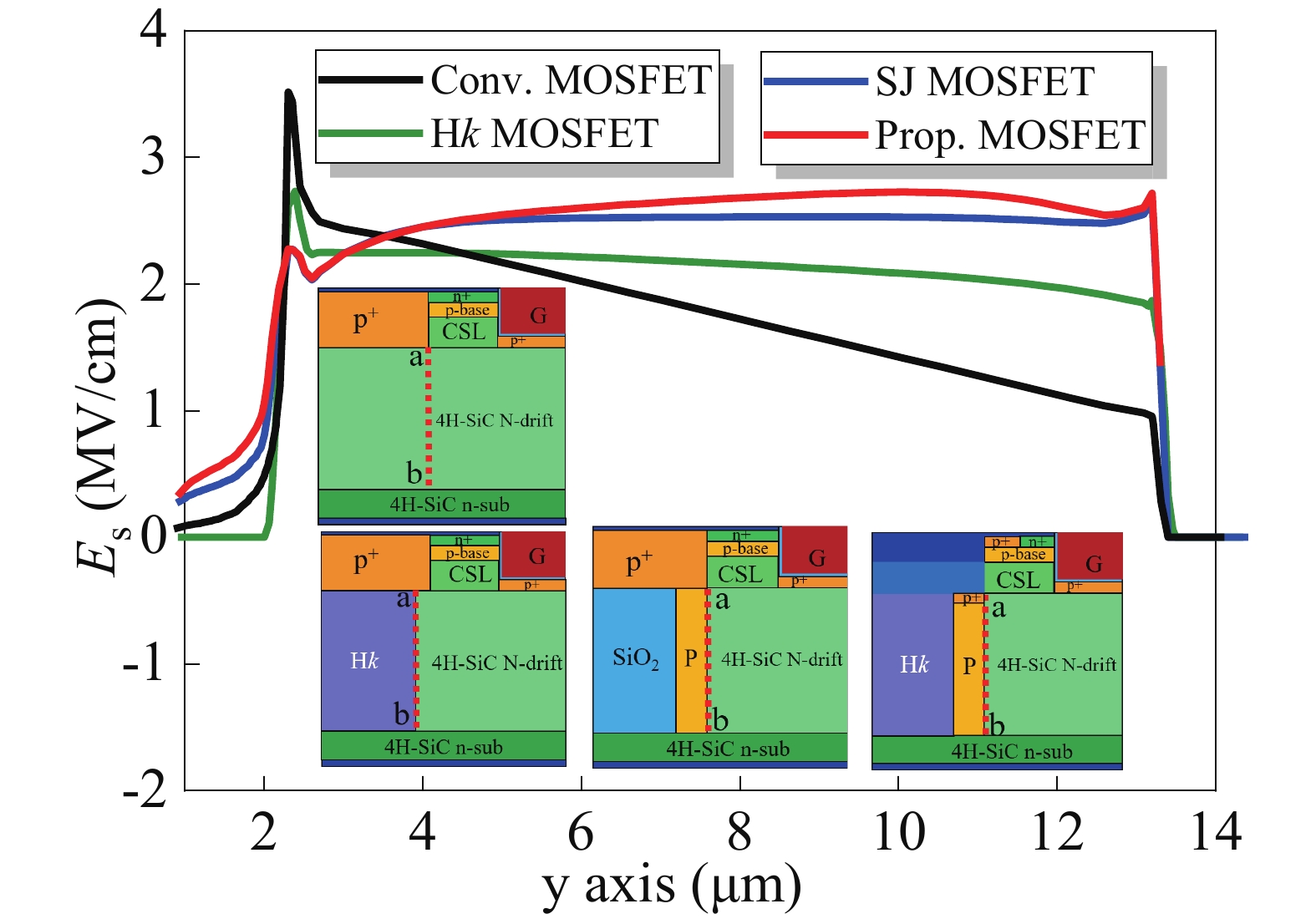

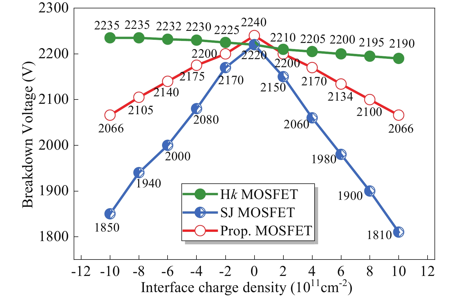

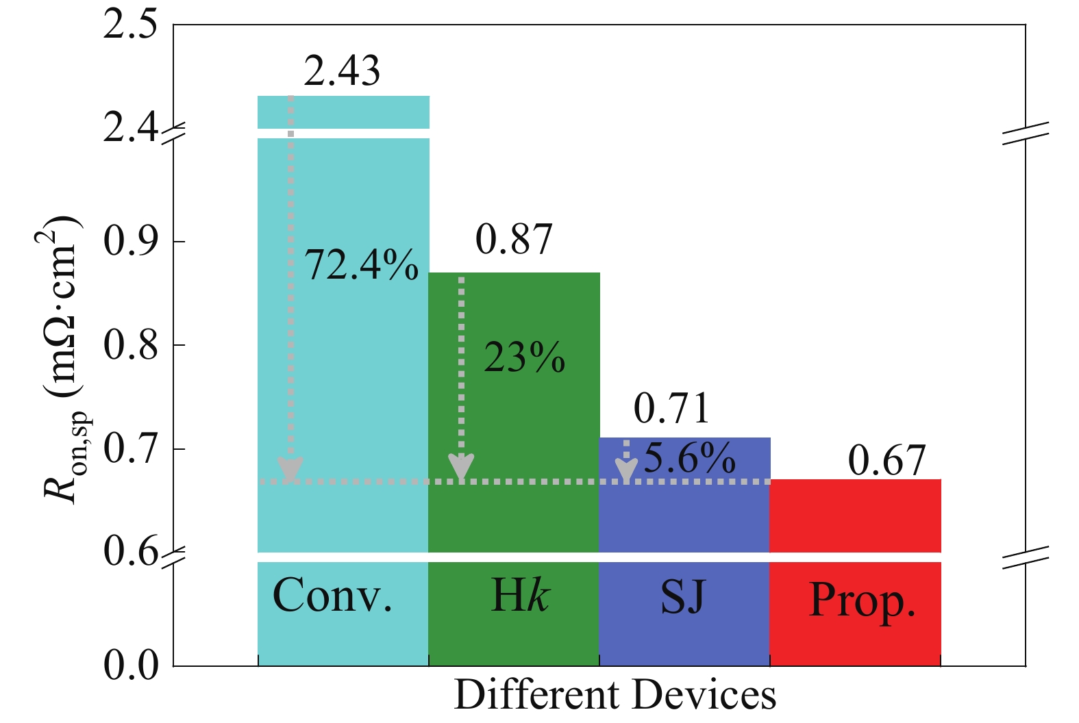
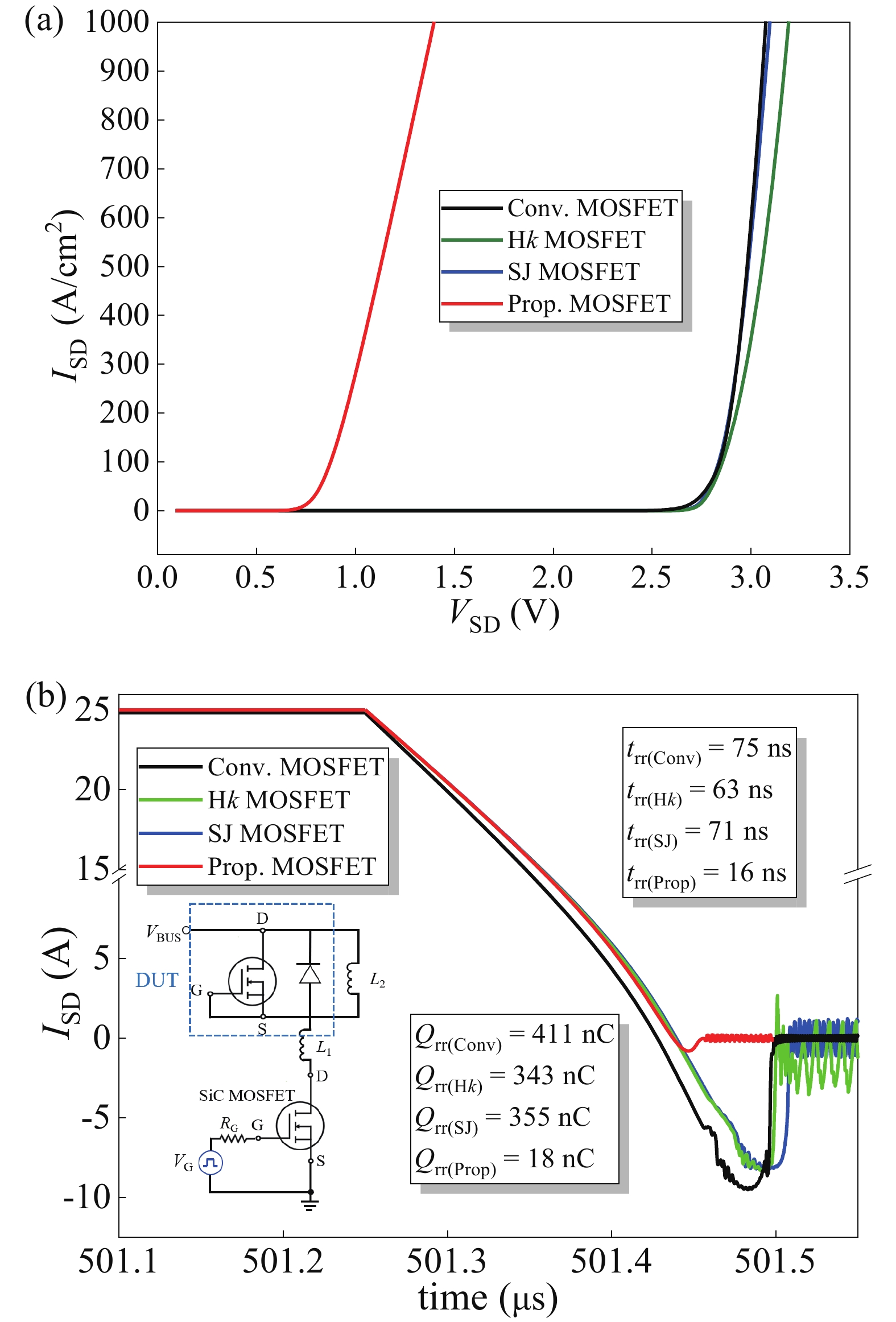
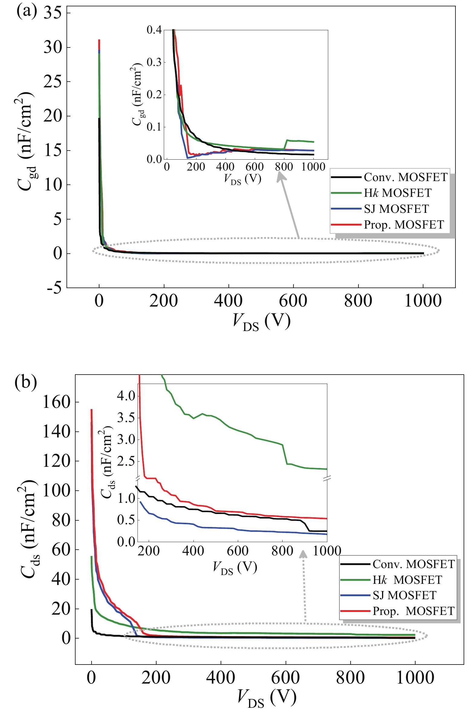
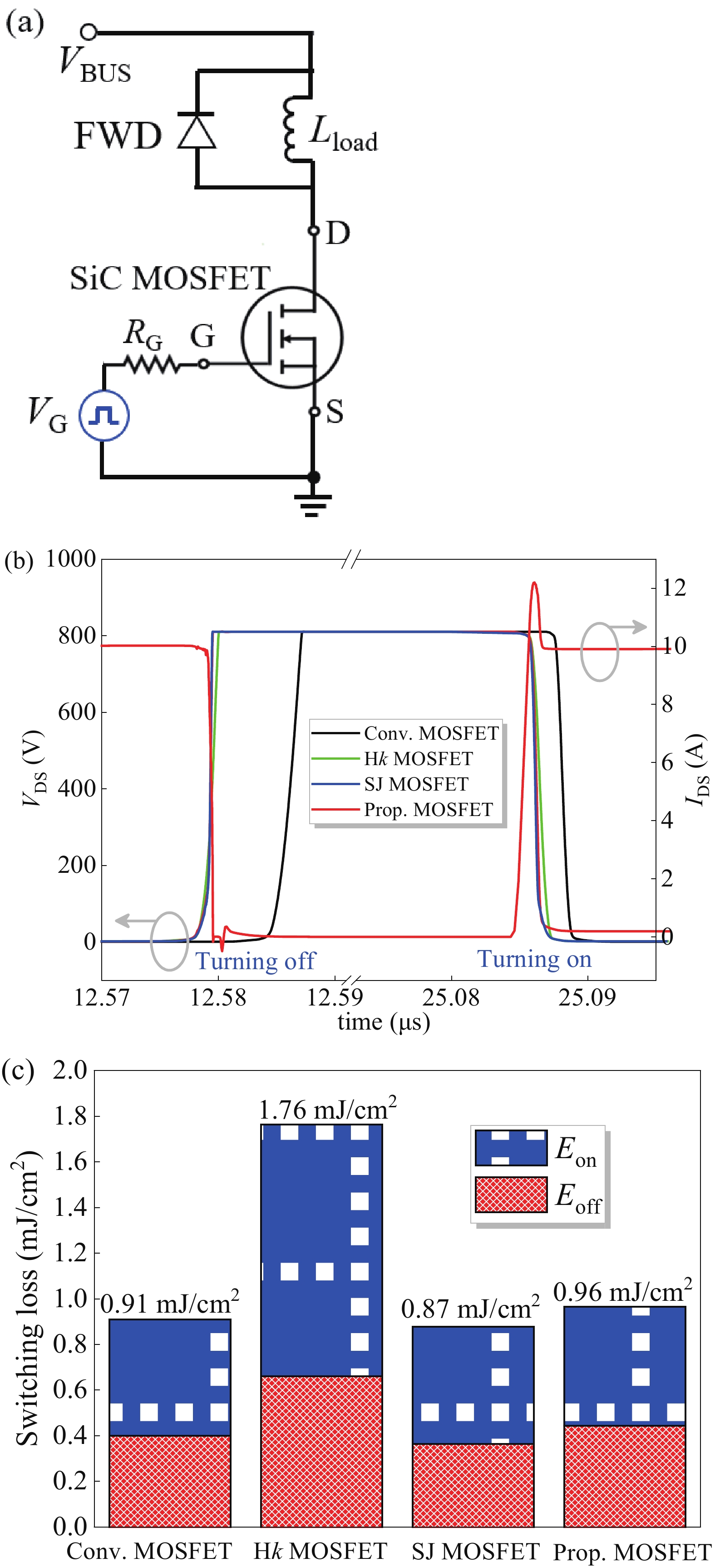
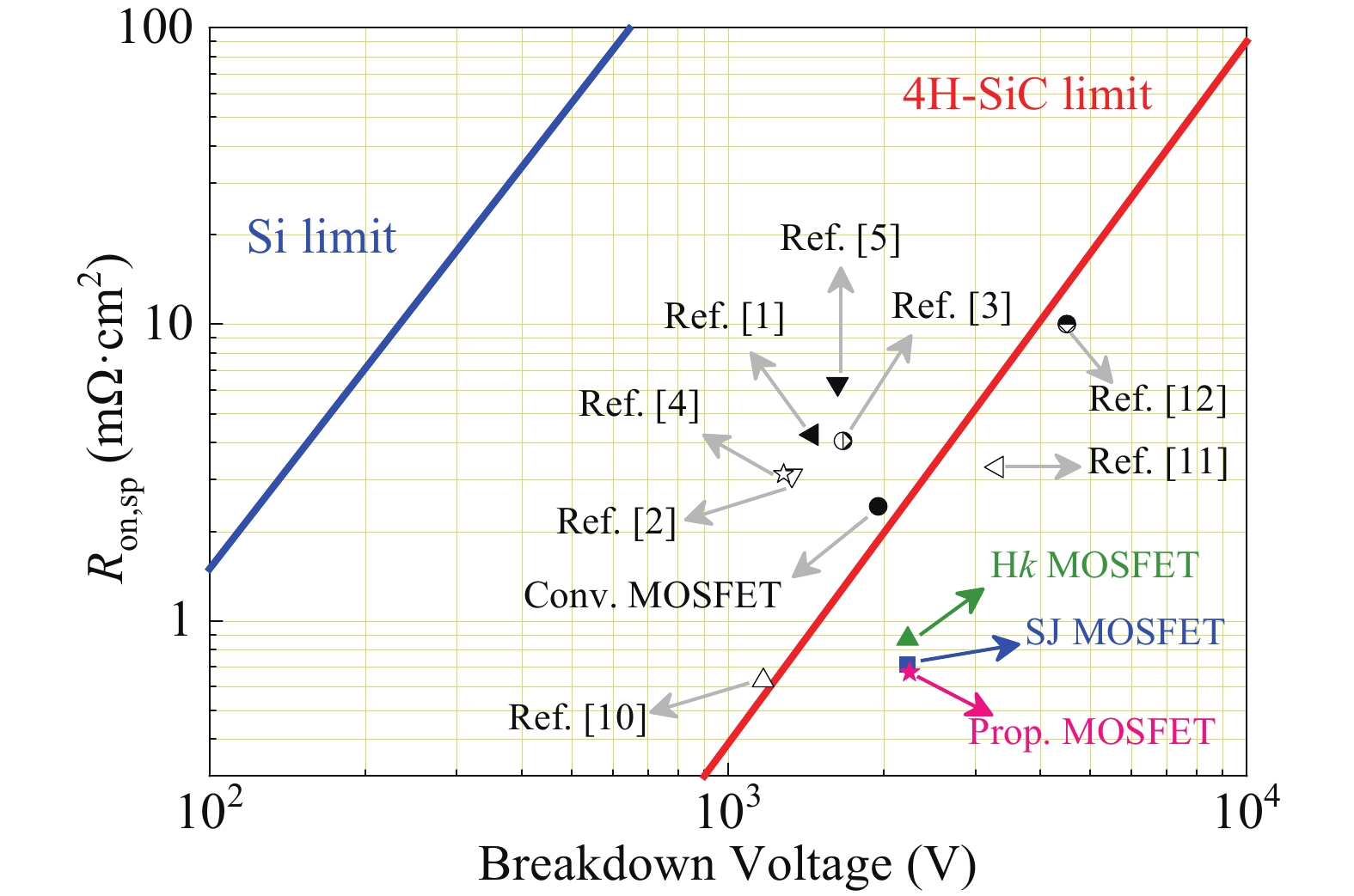
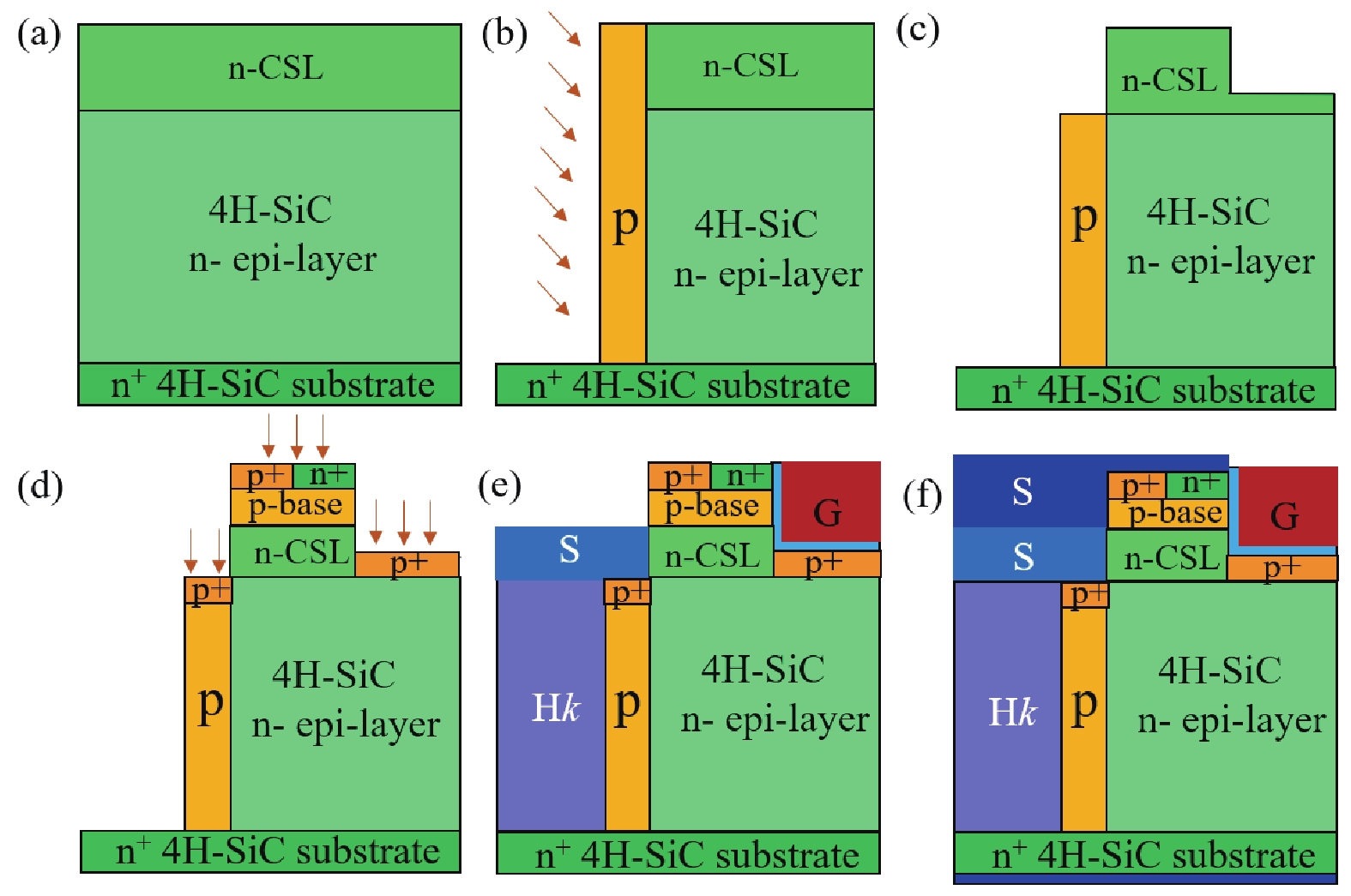
Table 1. Comparison between proposed Hk-SJ-SBD MOSFET, Hk MOSFET, SJ MOSFET and conventional MOSFET.
| Parameter | Conv. MOSFET | Hk MOSFET | SJ MOSFET | Prop. MOSFET |
| BV (V) | 1950 | 2220 | 2220 | 2240 |
| Ron,sp (mΩ·cm2) | 2.43 | 0.87 | 0.71 | 0.67 |
| Eon+ Eoff (mJ/cm2) | 0.91 | 1.76 | 0.87 | 0.96 |
| trr (ns) | 75 | 63 | 71 | 16 |
| Irrm (A) | 9.5 | 8.3 | 8.2 | 1.9 |
| Qrr (nC) | 411 | 343 | 355 | 18 |
| FOM (MV/cm2) | 1565 | 5665 | 6941 | 7489 |
 DownLoad: CSV
| [1] |
Oraon A, Shreya S, Kumari R, et al. A double trench 4H-SiC MOSFET as an enhanced model of SiC UMOSFET. 2017 7th International Symposium on Embedded Computing and System Design (ISED), 2018, 1 doi: 10.1109/ISED.2017.8303939
|
| [2] |
Yu H Y, Liang S W, Liu H Z, et al. Numerical study of SiC MOSFET with integrated n-/ n-type poly-Si/SiC heterojunction freewheeling diode. IEEE Trans Electron Devices, 2021, 68, 4571 doi: 10.1109/TED.2021.3097979
|
| [3] |
Huang H, Wang Y, Yu C H, et al. A high-performance SiC super-junction MOSFET with a step-doping profile. IEEE J Electron Devices Soc, 2021, 9, 1084 doi: 10.1109/JEDS.2021.3125706
|
| [4] |
Vudumula P, Kotamraju S. Design and optimization of 1.2-kV SiC planar inversion MOSFET using split dummy gate concept for high-frequency applications. IEEE Trans Electron Devices, 2019, 66, 5266 doi: 10.1109/TED.2019.2949459
|
| [5] |
Han K, Baliga B J, Sung W. Split-gate 1.2-kV 4H-SiC MOSFET: Analysis and experimental validation. IEEE Electron Device Lett, 2017, 38, 1437 doi: 10.1109/LED.2017.2738616
|
| [6] |
Kong M F, Hu Z W, Gao J C, et al. A 1200-V-class ultra-low specific on-resistance SiC lateral MOSFET with double trench gate and VLD technique. IEEE J Electron Devices Soc, 2021, 10, 83 doi: 10.1109/JEDS.2021.3136341
|
| [7] |
Liu Y T, Jin D H, Jiang S Q, et al. An active damping control method for the LLCL filter-based SiC MOSFET grid-connected inverter in vehicle-to-grid application. IEEE Trans Veh Technol, 2019, 68, 3411 doi: 10.1109/TVT.2019.2899166
|
| [8] |
Kim H, Chen H, Maksimović D, et al. SiC-MOSFET composite boost converter with 22 kW/L power density for electric vehicle application. 2017 IEEE Applied Power Electronics Conference and Exposition (APEC), 2017, 134 doi: 10.1109/APEC.2017.7930684
|
| [9] |
Anthon A, Zhang Z, Andersen M A E, et al. The benefits of SiC mosfets in a T-type inverter for grid-Tie applications. IEEE Trans Power Electron, 2016, 32, 2808 doi: 10.1109/TPEL.2016.2582344
|
| [10] |
Masuda T, Saito Y, Kumazawa T, et al. 0.63 mΩcm2 /1170V 4H H-SiC super junction V-groove trench MOSFET. 2018 IEEE International Electron Devices Meeting (IEDM), 2018, 484 doi: 10.1109/IEDM.2018.8614610
|
| [11] |
Baba M, Tawara T, Morimoto T, et al. Ultra-low specific on-resistance achieved in 3.3 kV-class SiC superjunction MOSFET. 2021 33rd International Symposium on Power Semiconductor Devices and ICs (ISPSD), 2021, 83 doi: 10.23919/ISPSD50666.2021.9452273
|
| [12] |
Ghandi R, Bolotnikov A, Kennerly S, et al. 4.5kV SiC charge-balanced MOSFETs with ultra-low on-resistance. 2020 32nd International Symposium on Power Semiconductor Devices and ICs (ISPSD), 2020, 126 doi: 10.1109/ISPSD46842.2020.9170171
|
| [13] |
Akshay K, Karmalkar S. Quick design of a superjunction considering charge imbalance due to process variations. IEEE Trans Electron Devices, 2020, 67, 3024 doi: 10.1109/TED.2020.2998443
|
| [14] |
Alam M, Morisette D T, Cooper J A. Design guidelines for superjunction devices in the presence of charge imbalance. IEEE Trans Electron Devices, 2018, 65, 3345 doi: 10.1109/TED.2018.2848584
|
| [15] |
Chen X B, Huang M M. A vertical power MOSFET with an interdigitated drift region using high-k insulator. IEEE Trans Electron Devices, 2012, 59, 2430 doi: 10.1109/TED.2012.2204890
|
| [16] |
Lyu X J, Chen X B. Vertical power Hk-MOSFET of hexagonal layout. IEEE Trans Electron Devices, 2013, 60, 1709 doi: 10.1109/TED.2013.2249068
|
| [17] |
Luo xiao rong, Cai jin yong, Fan Y, et al. Novel low-resistance current path UMOS with high-K dielectric Pillars. IEEE Trans Electron Devices, 2013, 60, 2840 doi: 10.1109/TED.2013.2272086
|
| [18] |
Naugarhiya A, Kondekar P N. High permittivity material selection for design of optimum Hk VDMOS. Superlattices Microstruct, 2015, 83, 310 doi: 10.1016/j.spmi.2015.02.045
|
| [19] |
He Z C, Cao M H, Wang N N, et al. Electron-pinned defect-dipoles for SrTiO3-based ceramics with high permittivity and low dielectric loss. 2016 Joint IEEE International Symposium on the Applications of Ferroelectrics, European Conference on Application of Polar Dielectrics, and Piezoelectric Force Microscopy Workshop (ISAF/ECAPD/PFM), 2016, 1 doi: https://doi.org/10.1109/ISAF.2016.7578071
|
| [20] |
Xia Z B, Chandrasekar H, Moore W, et al. Metal/BaTiO3/β-Ga2O3 dielectric heterojunction diode with 5.7 MV/cm breakdown field. Appl Phys Lett, 2019, 115, 252104 doi: 10.1063/1.5130669
|
| [21] |
Li J H, Li P, Huo W R, et al. Analysis and fabrication of an LDMOS with high-permittivity dielectric. IEEE Electron Device Lett, 2011, 32, 1266 doi: 10.1109/LED.2011.2158383
|
| [22] |
Yang H, Hu S D, Ran S L, et al. Simulative researching of a 1200V SiC trench MOSFET with an enhanced vertical RESURF effect. IEEE J Electron Devices Soc, 2020, 8, 1335 doi: 10.1109/JEDS.2020.3032649
|
| [23] |
Kitai H, Yamaguchi T, Hozumi Y, et al. A superior 15 kV SiC MOSFET with current spreading layer for high-frequency applications. Jpn J Appl Phys, 2019, 58, SBBD16 doi: 10.7567/1347-4065/ab01d1
|
| [24] |
Zheng Y L, Tang W M, Chau T, et al. Simulation study of 4H-SiC high-k pillar MOSFET with integrated Schottky barrier diode. IEEE J Electron Devices Soc, 2021, 9, 951 doi: 10.1109/JEDS.2021.3116715
|
| [25] |
Wang H Y, Wang C, Wang B Z, et al. 4H-SiC super-junction JFET: Design and experimental demonstration. IEEE Electron Device Lett, 2020, 41, 445 doi: 10.1109/LED.2020.2969683
|
| [26] |
Yano H, Nakao H, Mikami H, et al. Anomalously anisotropic channel mobility on trench sidewalls in 4H-SiC trench-gate metal-oxide-semiconductor field-effect transistors fabricated on 8° off substrates. Appl Phys Lett, 2007, 90, 042102 doi: 10.1063/1.2434157
|
| [27] |
Huang M M, Chen X B. A superjunction structure using high-kinsulator for power devices: Theory and optimization. J Semicond, 2016, 37, 064014 doi: 10.1088/1674-4926/37/6/064014
|
| [28] |
Zhao Y, Toyama M, Kita K, et al. Moisture-absorption-induced permittivity deterioration and surface roughness enhancement of lanthanum oxide films on silicon. Appl Phys Lett, 2006, 88, 072904 doi: 10.1063/1.2174840
|
| [29] |
Locquet J P, Marchiori C, Sousa M, et al. High-K dielectrics for the gate stack. J Appl Phys, 2006, 100, 051610 doi: 10.1063/1.2336996
|
| [30] |
Ji L F, Jiang Y J. Dielectric and microstructure modification of Ta2O5 ceramics by laser sintering. Mater Lett, 2006, 60, 86 doi: 10.1016/j.matlet.2005.07.077
|
| [31] |
Moon J H, Eom D I, No S Y, et al. Electrical properties of the La2O3/4H-SiC interface prepared by atomic layer deposition using La(iPrCp)3 and H2O. Mater Sci Forum, 2006, 527–529, 1083 doi: 10.4028/www.scientific.net/MSF.527-529.1083
|
| [32] |
Huang L H, Liu Y, Peng X, et al. Static performance and threshold voltage stability improvement of Al2O3/LaAlO3/SiO2 gate-stack for SiC power MOSFETs. IEEE Trans Electron Devices, 2022, 69, 690 doi: 10.1109/TED.2021.3138378
|
| [33] |
Yu J, Chen G, Li C X, et al. Hydrogen gas sensing properties of Pt/Ta2O5 Schottky diodes based on Si and SiC substrates. Sens Actuat A Phys, 2011, 172, 9 doi: 10.1016/j.sna.2011.02.021
|
| [34] |
Jinesh K B, Klootwijk J H, Lamy Y, et al. Enhanced electrical properties of atomic layer deposited La2O3 thin films with embedded ZrO2 nanocrystals. Appl Phys Lett, 2008, 93, 172904 doi: 10.1063/1.3009202
|
| [35] |
Kang S K, Ishiwara H. Characteristics of LaAlO3 as insulating buffer layers of ferroelectric-gate field effect transistors. Jpn J Appl Phys, 2002, 41, 6899 doi: 10.1143/JJAP.41.6899
|
| [36] |
Kao C H, Lai P L, Wang H Y. The comparison between Ta2O5 and Ti-doped Ta2O5 dielectrics. Surf Coat Technol, 2013, 231, 512 doi: 10.1016/j.surfcoat.2012.04.045
|
| [37] |
Agarwal A K, Seshadri S, Rowland L B. Temperature dependence of Fowler-Nordheim Current in 6H- and 4H-SiC MOS capacitors. IEEE Electron Device Lett, 1997, 18, 592 doi: 10.1109/55.644081
|
| [38] |
He Q Y, Luo X R, Liao T, et al. 4H-SiC superjunction trench MOSFET with reduced saturation current. Superlattices Microstruct, 2019, 125, 58 doi: 10.1016/j.spmi.2018.10.016
|
| [39] |
Wang Z G, Wang X, Kuo J B. Modeling power vertical high-k MOS device with interface charges via superposition methodology-breakdown voltage and specific ON-resistance. IEEE Trans Electron Devices, 2018, 65, 4947 doi: 10.1109/TED.2018.2870174
|
| [40] |
Noborio M, Jun S D, Kimoto T. P-channel MOSFETs on 4H-SiC {0001} and nonbasal faces fabricated by oxide deposition and N2O annealing. IEEE Trans Electron Devices, 2009, 56, 1953 doi: 10.1109/TED.2009.2025909
|
| [41] |
Pérez-Tomás A, Brosselard P, Hassan J, et al. Schottky versus bipolar 3.3 kV SiC diodes. Semicond Sci Technol, 2008, 23, 125004 doi: 10.1088/0268-1242/23/12/125004
|
| [42] |
Schilirò E, Lo Nigro R, Fiorenza P, et al. Negative charge trapping effects in Al2O3 films grown by atomic layer deposition onto thermally oxidized 4H-SiC. AIP Adv, 2016, 6, 075021 doi: 10.1063/1.4960213
|
| [43] |
Han S Y, Kim K H, Kim J K, et al. Ohmic contact formation mechanism of Ni on n-type 4H-SiC. Appl Phys Lett, 2001, 79, 1816 doi: 10.1063/1.1404998
|
| [44] |
Hatano M, Moon S, Lee M H, et al. In situ and ex situ diagnostics on melting and resolidification dynamics of amorphous and polycrystalline silicon thin films during excimer laser annealing. J Non Cryst Solids, 2000, 266–269, 654 doi: 10.1016/S0022-3093(99)00768-1
|
| [45] |
Pécz B. Contact formation in SiC devices. Appl Surf Sci, 2001, 184, 287 doi: 10.1016/S0169-4332(01)00678-X
|


Article views: 1627 Times PDF downloads: 219 Times Cited by: 0 Times
Received: 28 October 2022 Revised: 16 January 2023 Online: Accepted Manuscript: 08 February 2023Uncorrected proof: 09 February 2023Published: 10 May 2023
| Citation: |
Moufu Kong, Zewei Hu, Ronghe Yan, Bo Yi, Bingke Zhang, Hongqiang Yang. A novel SiC high-k superjunction power MOSFET integrated Schottky barrier diode with improved forward and reverse performance[J]. Journal of Semiconductors, 2023, 44(5): 052801. doi: 10.1088/1674-4926/44/5/052801
****
M F Kong, Z W Hu, R H Yan, B Yi, B K Zhang, H Q Yang. A novel SiC high-k superjunction power MOSFET integrated Schottky barrier diode with improved forward and reverse performance[J]. J. Semicond, 2023, 44(5): 052801. doi: 10.1088/1674-4926/44/5/052801

|
 Moufu Kong:received his Ph.D from the University of Electronic Science and Technology of China in 2013. He is now an associate professor at the University of Electronic Science and Technology of China. He was a visiting scholar at Nanyang Technological University (Singapore) from 2019 to 2020. His research focuses on smart power integrated circuits, high voltage power devices and wide-bandgap semiconductor power devices. He has published over 50 academic papers in Nat Commun, IEEE T-ED, IEEE EDL, SST, IEEE JEDS, etc. and IEEE international conferences. He served as a technical program committee member for technical conferences including IEEE ICSICT, IEEE ASICON, IEEE ISNE and IEEE EDTM, etc
| [1] |
Oraon A, Shreya S, Kumari R, et al. A double trench 4H-SiC MOSFET as an enhanced model of SiC UMOSFET. 2017 7th International Symposium on Embedded Computing and System Design (ISED), 2018, 1 doi: 10.1109/ISED.2017.8303939
|
| [2] |
Yu H Y, Liang S W, Liu H Z, et al. Numerical study of SiC MOSFET with integrated n-/ n-type poly-Si/SiC heterojunction freewheeling diode. IEEE Trans Electron Devices, 2021, 68, 4571 doi: 10.1109/TED.2021.3097979
|
| [3] |
Huang H, Wang Y, Yu C H, et al. A high-performance SiC super-junction MOSFET with a step-doping profile. IEEE J Electron Devices Soc, 2021, 9, 1084 doi: 10.1109/JEDS.2021.3125706
|
| [4] |
Vudumula P, Kotamraju S. Design and optimization of 1.2-kV SiC planar inversion MOSFET using split dummy gate concept for high-frequency applications. IEEE Trans Electron Devices, 2019, 66, 5266 doi: 10.1109/TED.2019.2949459
|
| [5] |
Han K, Baliga B J, Sung W. Split-gate 1.2-kV 4H-SiC MOSFET: Analysis and experimental validation. IEEE Electron Device Lett, 2017, 38, 1437 doi: 10.1109/LED.2017.2738616
|
| [6] |
Kong M F, Hu Z W, Gao J C, et al. A 1200-V-class ultra-low specific on-resistance SiC lateral MOSFET with double trench gate and VLD technique. IEEE J Electron Devices Soc, 2021, 10, 83 doi: 10.1109/JEDS.2021.3136341
|
| [7] |
Liu Y T, Jin D H, Jiang S Q, et al. An active damping control method for the LLCL filter-based SiC MOSFET grid-connected inverter in vehicle-to-grid application. IEEE Trans Veh Technol, 2019, 68, 3411 doi: 10.1109/TVT.2019.2899166
|
| [8] |
Kim H, Chen H, Maksimović D, et al. SiC-MOSFET composite boost converter with 22 kW/L power density for electric vehicle application. 2017 IEEE Applied Power Electronics Conference and Exposition (APEC), 2017, 134 doi: 10.1109/APEC.2017.7930684
|
| [9] |
Anthon A, Zhang Z, Andersen M A E, et al. The benefits of SiC mosfets in a T-type inverter for grid-Tie applications. IEEE Trans Power Electron, 2016, 32, 2808 doi: 10.1109/TPEL.2016.2582344
|
| [10] |
Masuda T, Saito Y, Kumazawa T, et al. 0.63 mΩcm2 /1170V 4H H-SiC super junction V-groove trench MOSFET. 2018 IEEE International Electron Devices Meeting (IEDM), 2018, 484 doi: 10.1109/IEDM.2018.8614610
|
| [11] |
Baba M, Tawara T, Morimoto T, et al. Ultra-low specific on-resistance achieved in 3.3 kV-class SiC superjunction MOSFET. 2021 33rd International Symposium on Power Semiconductor Devices and ICs (ISPSD), 2021, 83 doi: 10.23919/ISPSD50666.2021.9452273
|
| [12] |
Ghandi R, Bolotnikov A, Kennerly S, et al. 4.5kV SiC charge-balanced MOSFETs with ultra-low on-resistance. 2020 32nd International Symposium on Power Semiconductor Devices and ICs (ISPSD), 2020, 126 doi: 10.1109/ISPSD46842.2020.9170171
|
| [13] |
Akshay K, Karmalkar S. Quick design of a superjunction considering charge imbalance due to process variations. IEEE Trans Electron Devices, 2020, 67, 3024 doi: 10.1109/TED.2020.2998443
|
| [14] |
Alam M, Morisette D T, Cooper J A. Design guidelines for superjunction devices in the presence of charge imbalance. IEEE Trans Electron Devices, 2018, 65, 3345 doi: 10.1109/TED.2018.2848584
|
| [15] |
Chen X B, Huang M M. A vertical power MOSFET with an interdigitated drift region using high-k insulator. IEEE Trans Electron Devices, 2012, 59, 2430 doi: 10.1109/TED.2012.2204890
|
| [16] |
Lyu X J, Chen X B. Vertical power Hk-MOSFET of hexagonal layout. IEEE Trans Electron Devices, 2013, 60, 1709 doi: 10.1109/TED.2013.2249068
|
| [17] |
Luo xiao rong, Cai jin yong, Fan Y, et al. Novel low-resistance current path UMOS with high-K dielectric Pillars. IEEE Trans Electron Devices, 2013, 60, 2840 doi: 10.1109/TED.2013.2272086
|
| [18] |
Naugarhiya A, Kondekar P N. High permittivity material selection for design of optimum Hk VDMOS. Superlattices Microstruct, 2015, 83, 310 doi: 10.1016/j.spmi.2015.02.045
|
| [19] |
He Z C, Cao M H, Wang N N, et al. Electron-pinned defect-dipoles for SrTiO3-based ceramics with high permittivity and low dielectric loss. 2016 Joint IEEE International Symposium on the Applications of Ferroelectrics, European Conference on Application of Polar Dielectrics, and Piezoelectric Force Microscopy Workshop (ISAF/ECAPD/PFM), 2016, 1 doi: https://doi.org/10.1109/ISAF.2016.7578071
|
| [20] |
Xia Z B, Chandrasekar H, Moore W, et al. Metal/BaTiO3/β-Ga2O3 dielectric heterojunction diode with 5.7 MV/cm breakdown field. Appl Phys Lett, 2019, 115, 252104 doi: 10.1063/1.5130669
|
| [21] |
Li J H, Li P, Huo W R, et al. Analysis and fabrication of an LDMOS with high-permittivity dielectric. IEEE Electron Device Lett, 2011, 32, 1266 doi: 10.1109/LED.2011.2158383
|
| [22] |
Yang H, Hu S D, Ran S L, et al. Simulative researching of a 1200V SiC trench MOSFET with an enhanced vertical RESURF effect. IEEE J Electron Devices Soc, 2020, 8, 1335 doi: 10.1109/JEDS.2020.3032649
|
| [23] |
Kitai H, Yamaguchi T, Hozumi Y, et al. A superior 15 kV SiC MOSFET with current spreading layer for high-frequency applications. Jpn J Appl Phys, 2019, 58, SBBD16 doi: 10.7567/1347-4065/ab01d1
|
| [24] |
Zheng Y L, Tang W M, Chau T, et al. Simulation study of 4H-SiC high-k pillar MOSFET with integrated Schottky barrier diode. IEEE J Electron Devices Soc, 2021, 9, 951 doi: 10.1109/JEDS.2021.3116715
|
| [25] |
Wang H Y, Wang C, Wang B Z, et al. 4H-SiC super-junction JFET: Design and experimental demonstration. IEEE Electron Device Lett, 2020, 41, 445 doi: 10.1109/LED.2020.2969683
|
| [26] |
Yano H, Nakao H, Mikami H, et al. Anomalously anisotropic channel mobility on trench sidewalls in 4H-SiC trench-gate metal-oxide-semiconductor field-effect transistors fabricated on 8° off substrates. Appl Phys Lett, 2007, 90, 042102 doi: 10.1063/1.2434157
|
| [27] |
Huang M M, Chen X B. A superjunction structure using high-kinsulator for power devices: Theory and optimization. J Semicond, 2016, 37, 064014 doi: 10.1088/1674-4926/37/6/064014
|
| [28] |
Zhao Y, Toyama M, Kita K, et al. Moisture-absorption-induced permittivity deterioration and surface roughness enhancement of lanthanum oxide films on silicon. Appl Phys Lett, 2006, 88, 072904 doi: 10.1063/1.2174840
|
| [29] |
Locquet J P, Marchiori C, Sousa M, et al. High-K dielectrics for the gate stack. J Appl Phys, 2006, 100, 051610 doi: 10.1063/1.2336996
|
| [30] |
Ji L F, Jiang Y J. Dielectric and microstructure modification of Ta2O5 ceramics by laser sintering. Mater Lett, 2006, 60, 86 doi: 10.1016/j.matlet.2005.07.077
|
| [31] |
Moon J H, Eom D I, No S Y, et al. Electrical properties of the La2O3/4H-SiC interface prepared by atomic layer deposition using La(iPrCp)3 and H2O. Mater Sci Forum, 2006, 527–529, 1083 doi: 10.4028/www.scientific.net/MSF.527-529.1083
|
| [32] |
Huang L H, Liu Y, Peng X, et al. Static performance and threshold voltage stability improvement of Al2O3/LaAlO3/SiO2 gate-stack for SiC power MOSFETs. IEEE Trans Electron Devices, 2022, 69, 690 doi: 10.1109/TED.2021.3138378
|
| [33] |
Yu J, Chen G, Li C X, et al. Hydrogen gas sensing properties of Pt/Ta2O5 Schottky diodes based on Si and SiC substrates. Sens Actuat A Phys, 2011, 172, 9 doi: 10.1016/j.sna.2011.02.021
|
| [34] |
Jinesh K B, Klootwijk J H, Lamy Y, et al. Enhanced electrical properties of atomic layer deposited La2O3 thin films with embedded ZrO2 nanocrystals. Appl Phys Lett, 2008, 93, 172904 doi: 10.1063/1.3009202
|
| [35] |
Kang S K, Ishiwara H. Characteristics of LaAlO3 as insulating buffer layers of ferroelectric-gate field effect transistors. Jpn J Appl Phys, 2002, 41, 6899 doi: 10.1143/JJAP.41.6899
|
| [36] |
Kao C H, Lai P L, Wang H Y. The comparison between Ta2O5 and Ti-doped Ta2O5 dielectrics. Surf Coat Technol, 2013, 231, 512 doi: 10.1016/j.surfcoat.2012.04.045
|
| [37] |
Agarwal A K, Seshadri S, Rowland L B. Temperature dependence of Fowler-Nordheim Current in 6H- and 4H-SiC MOS capacitors. IEEE Electron Device Lett, 1997, 18, 592 doi: 10.1109/55.644081
|
| [38] |
He Q Y, Luo X R, Liao T, et al. 4H-SiC superjunction trench MOSFET with reduced saturation current. Superlattices Microstruct, 2019, 125, 58 doi: 10.1016/j.spmi.2018.10.016
|
| [39] |
Wang Z G, Wang X, Kuo J B. Modeling power vertical high-k MOS device with interface charges via superposition methodology-breakdown voltage and specific ON-resistance. IEEE Trans Electron Devices, 2018, 65, 4947 doi: 10.1109/TED.2018.2870174
|
| [40] |
Noborio M, Jun S D, Kimoto T. P-channel MOSFETs on 4H-SiC {0001} and nonbasal faces fabricated by oxide deposition and N2O annealing. IEEE Trans Electron Devices, 2009, 56, 1953 doi: 10.1109/TED.2009.2025909
|
| [41] |
Pérez-Tomás A, Brosselard P, Hassan J, et al. Schottky versus bipolar 3.3 kV SiC diodes. Semicond Sci Technol, 2008, 23, 125004 doi: 10.1088/0268-1242/23/12/125004
|
| [42] |
Schilirò E, Lo Nigro R, Fiorenza P, et al. Negative charge trapping effects in Al2O3 films grown by atomic layer deposition onto thermally oxidized 4H-SiC. AIP Adv, 2016, 6, 075021 doi: 10.1063/1.4960213
|
| [43] |
Han S Y, Kim K H, Kim J K, et al. Ohmic contact formation mechanism of Ni on n-type 4H-SiC. Appl Phys Lett, 2001, 79, 1816 doi: 10.1063/1.1404998
|
| [44] |
Hatano M, Moon S, Lee M H, et al. In situ and ex situ diagnostics on melting and resolidification dynamics of amorphous and polycrystalline silicon thin films during excimer laser annealing. J Non Cryst Solids, 2000, 266–269, 654 doi: 10.1016/S0022-3093(99)00768-1
|
| [45] |
Pécz B. Contact formation in SiC devices. Appl Surf Sci, 2001, 184, 287 doi: 10.1016/S0169-4332(01)00678-X
|

 WeChat ID
Journal of Semiconductors © 2017 All Rights Reserved 京ICP备05085259号-2


