| [1] |
Baliga B J. Fundamentals of power semiconductor devices. Cham: Springer International Publishing, 2019
|
| [2] |
Wong M H, Higashiwaki M. Vertical β-Ga 2O 3 power transistors: A review. IEEE Trans Electron Devices, 2020, 67, 3925 doi: 10.1109/TED.2020.3016609 |
| [3] |
She X, Huang A Q, Lucía Ó, et al. Review of silicon carbide power devices and their applications. IEEE Trans Ind Electron, 2017, 64, 8193 doi: 10.1109/TIE.2017.2652401 |
| [4] |
Sun R Z, Lai J X, Chen W J, et al. GaN power integration for high frequency and high efficiency power applications: A review. IEEE Access, 2020, 8, 15529 doi: 10.1109/ACCESS.2020.2967027 |
| [5] |
Wang C L, Zhang J C, Xu S R, et al. Progress in state-of-the-art technologies of Ga 2O 3 devices. J Phys D, 2021, 54, 243001 doi: 10.1088/1361-6463/abe158 |
| [6] |
Higashiwaki M, Sasaki K, Kuramata A, et al. Gallium oxide (Ga 2O 3) metal-semiconductor field-effect transistors on single-crystal β-Ga 2O 3 (010) substrates. Appl Phys Lett, 2012, 100, 013504 doi: 10.1063/1.3674287 |
| [7] |
Wagner G, Baldini M, Gogova D, et al. Homoepitaxial growth of β-Ga 2O 3 layers by metal-organic vapor phase epitaxy. Phys Status Solidi A, 2014, 211, 27 doi: 10.1002/pssa.201330092 |
| [8] |
Baldini M, Albrecht M, Fiedler A, et al. Si- and Sn-doped homoepitaxial β-Ga 2O 3 layers grown by MOVPE on (010)-oriented substrates. ECS J Solid State Sci Technol, 2016, 6, Q3040 doi: 10.1149/2.0081702jss |
| [9] |
Zhang Y W, Alema F, Mauze A, et al. MOCVD grown epitaxial β-Ga 2O 3 thin film with an electron mobility of 176 cm 2/V s at room temperature. APL Mater, 2019, 7, 022506 doi: 10.1063/1.5058059 |
| [10] |
Oshima T, Arai N, Suzuki N, et al. Surface morphology of homoepitaxial β-Ga 2O 3 thin films grown by molecular beam epitaxy. Thin Solid Films, 2008, 516, 5768 doi: 10.1016/j.tsf.2007.10.045 |
| [11] |
Sasaki K, Higashiwaki M, Kuramata A, et al. Growth temperature dependences of structural and electrical properties of Ga 2O 3 epitaxial films grown on β-Ga 2O 3 (010) substrates by molecular beam epitaxy. J Cryst Growth, 2014, 392, 30 doi: 10.1016/j.jcrysgro.2014.02.002 |
| [12] |
Nomura K, Goto K, Togashi R, et al. Thermodynamic study of β-Ga 2O 3 growth by halide vapor phase epitaxy. J Cryst Growth, 2014, 405, 19 doi: 10.1016/j.jcrysgro.2014.06.051 |
| [13] |
Oshima Y, Vίllora E G, Shimamura K. Quasi-heteroepitaxial growth of β-Ga 2O 3 on off-angled sapphire (0001) substrates by halide vapor phase epitaxy. J Cryst Growth, 2015, 410, 53 doi: 10.1016/j.jcrysgro.2014.10.038 |
| [14] |
Leach J H, Udwary K, Rumsey J, et al. Halide vapor phase epitaxial growth of β-Ga 2O 3 and α-Ga 2O 3 films. APL Mater, 2019, 7, 022504 doi: 10.1063/1.5055680 |
| [15] |
Ueda N, Hosono H, Waseda R, et al. Synthesis and control of conductivity of ultraviolet transmitting β-Ga 2O 3 single crystals. Appl Phys Lett, 1997, 70, 3561 doi: 10.1063/1.119233 |
| [16] |
Sasaki K, Kuramata A, Masui T, et al. Device-quality β-Ga 2O 3 epitaxial films fabricated by ozone molecular beam epitaxy. Appl Phys Express, 2012, 5, 035502 doi: 10.1143/APEX.5.035502 |
| [17] |
Han S H, Mauze A, Ahmadi E, et al. n-type dopants in (001) β-Ga 2O 3 grown on (001) β-Ga 2O 3 substrates by plasma-assisted molecular beam epitaxy. Semicond Sci Technol, 2018, 33, 045001 doi: 10.1088/1361-6641/aaae56 |
| [18] |
Víllora E G, Shimamura K, Yoshikawa Y, et al. Electrical conductivity and carrier concentration control in β-Ga 2O 3 by Si doping. Appl Phys Lett, 2008, 92, 202120 doi: 10.1063/1.2919728 |
| [19] |
Gogova D, Wagner G, Baldini M, et al. Structural properties of Si-doped β-Ga 2O 3 layers grown by MOVPE. J Cryst Growth, 2014, 401, 665 doi: 10.1016/j.jcrysgro.2013.11.056 |
| [20] |
Ahmadi E, Koksaldi O S, Kaun S W, et al. Ge doping of β-Ga 2O 3 films grown by plasma-assisted molecular beam epitaxy. Appl Phys Express, 2017, 10, 041102 doi: 10.7567/APEX.10.041102 |
| [21] |
Saleh M, Bhattacharyya A, Varley J B, et al. Electrical and optical properties of Zr doped β-Ga 2O 3 single crystals. Appl Phys Express, 2019, 12, 085502 doi: 10.7567/1882-0786/ab2b6c |
| [22] |
Saleh M, Varley J B, Jesenovec J, et al. Degenerate doping in β-Ga 2O 3 single crystals through Hf-doping. Semicond Sci Technol, 2020, 35, 04LT01 doi: 10.1088/1361-6641/ab75a6 |
| [23] |
Wong M H, Sasaki K, Kuramata A, et al. Field-plated Ga 2O 3 MOSFETs with a breakdown voltage of over 750 V. IEEE Electron Device Lett, 2016, 37, 212 doi: 10.1109/LED.2015.2512279 |
| [24] |
Lv Y J, Zhou X Y, Long S B, et al. Source-field-plated β-Ga 2O 3 MOSFET with record power figure of merit of 50.4 MW/cm 2. IEEE Electron Device Lett, 2019, 40, 83 doi: 10.1109/LED.2018.2881274 |
| [25] |
Sharma S, Zeng K, Saha S, et al. Field-plated lateral Ga 2O 3 MOSFETs with polymer passivation and 8.03 kV breakdown voltage. IEEE Electron Device Lett, 2020, 41, 836 doi: 10.1109/LED.2020.2991146 |
| [26] |
Kanechika M, Sugimoto M, Soejima N, et al. A vertical insulated gate AlGaN/GaN heterojunction field-effect transistor. Jpn J Appl Phys, 2007, 46, L503 doi: 10.1143/JJAP.46.L503 |
| [27] |
Shenoy J N, Cooper J A, Melloch M R. High-voltage double-implanted power MOSFET’s in 6H-SiC. IEEE Electron Device Lett, 1997, 18, 93 doi: 10.1109/55.556091 |
| [28] |
Kyrtsos A, Matsubara M, Bellotti E. On the feasibility of p-type Ga 2O 3. Appl Phys Lett, 2018, 112, 032108 doi: 10.1063/1.5009423 |
| [29] |
Chabak K D, McCandless J P, Moser N A, et al. Recessed-gate enhancement-mode β-Ga 2O 3 MOSFETs. IEEE Electron Device Lett, 2018, 39, 67 doi: 10.1109/LED.2017.2779867 |
| [30] |
Feng Z Q, Cai Y C, Li Z, et al. Design and fabrication of field-plated normally off β-Ga 2O 3 MOSFET with laminated-ferroelectric charge storage gate for high power application. Appl Phys Lett, 2020, 116, 243503 doi: 10.1063/5.0010561 |
| [31] |
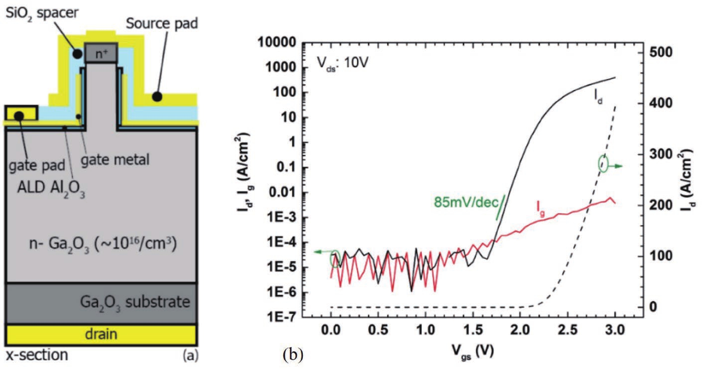
Kamimura T, Nakata Y, Wong M H, et al. Normally-off Ga 2O 3 MOSFETs with unintentionally nitrogen-doped channel layer grown by plasma-assisted molecular beam epitaxy. IEEE Electron Device Lett, 2019, 40, 1064 doi: 10.1109/LED.2019.2919251 |
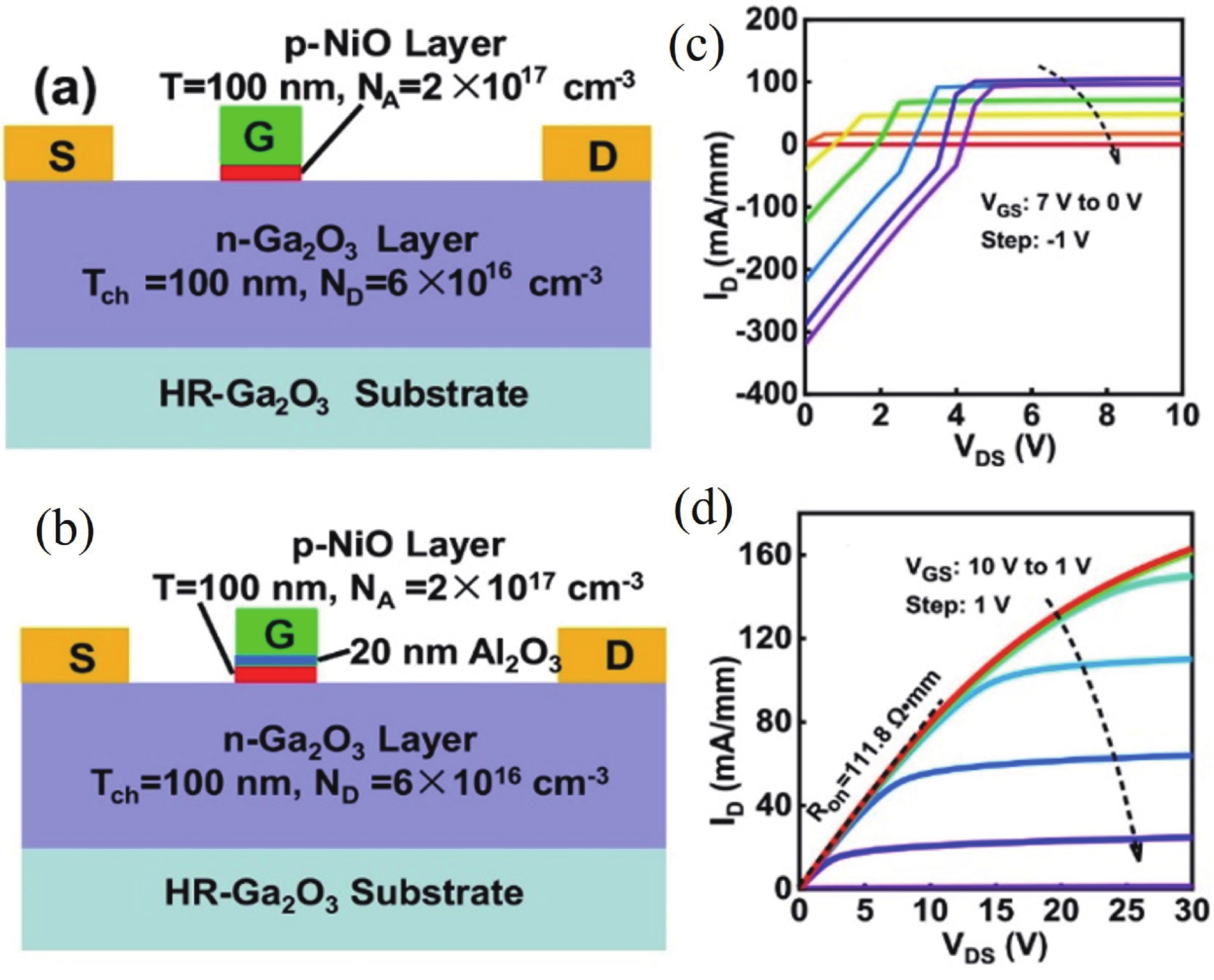
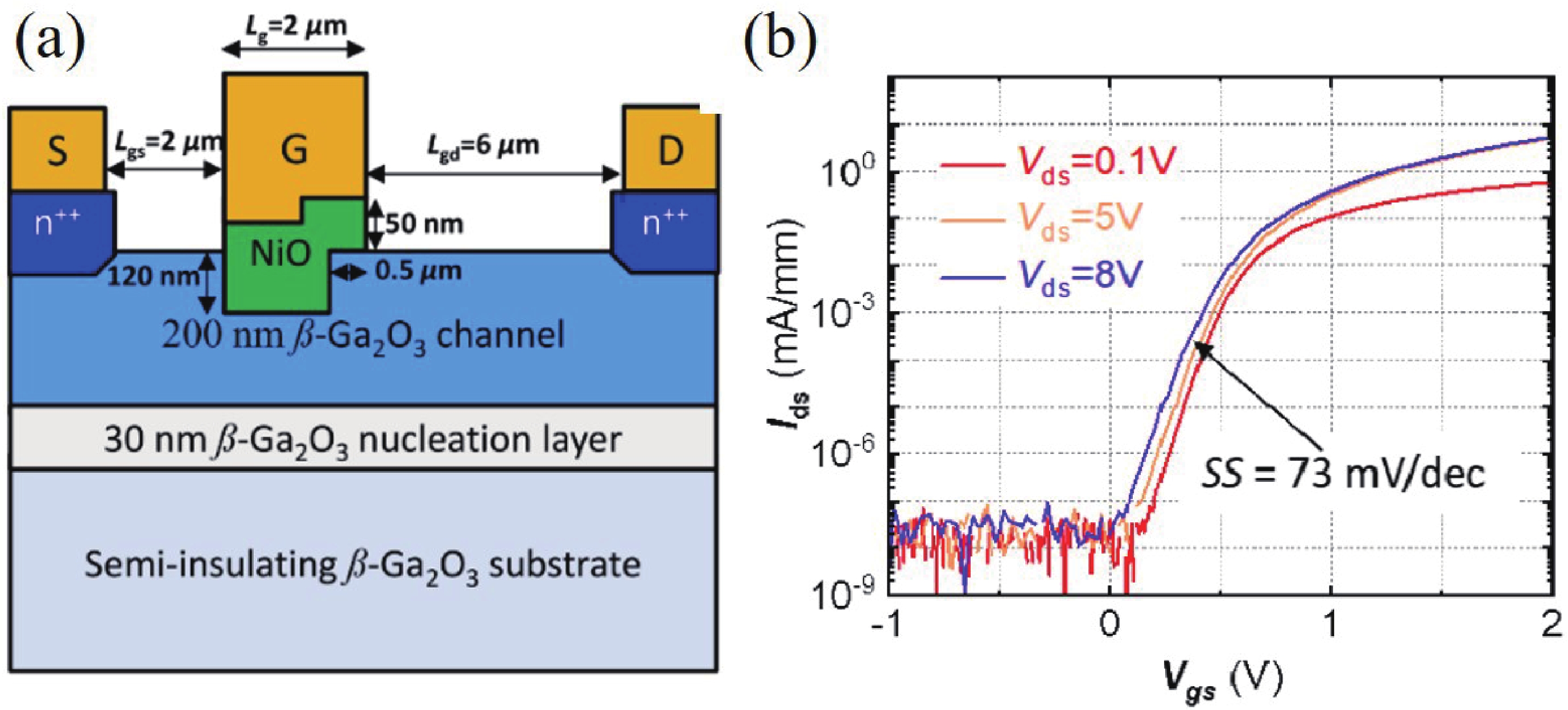
| [32] |
Zhou X Z, Liu Q, Hao W B, et al. Normally-off β-Ga 2O 3 power heterojunction field-effect-transistor realized by p-NiO and recessed-gate. 2022 IEEE 34th International Symposium on Power Semiconductor Devices and ICs (ISPSD), 2022, 101 doi: 10.1109/ISPSD49238.2022.9813678 |
| [33] |
Feng Z X, Anhar Uddin Bhuiyan A F M, Karim M R, et al. MOCVD homoepitaxy of Si-doped (010) β-Ga 2O 3 thin films with superior transport properties. Appl Phys Lett, 2019, 114, 250601 doi: 10.1063/1.5109678 |
| [34] |
Seryogin G, Alema F, Valente N, et al. MOCVD growth of high purity Ga 2O 3 epitaxial films using trimethylgallium precursor. Appl Phys Lett, 2020, 117, 262101 doi: 10.1063/5.0031484 |
| [35] |
Zhang T, Li Y F, Cheng Q, et al. Influence of O 2 pulse on the β-Ga 2O 3 films deposited by pulsed MOCVD. Ceram Int, 2022, 48, 8268 doi: 10.1016/j.ceramint.2021.12.031 |
| [36] |
Hernandez A, Islam M M, Saddatkia P, et al. MOCVD growth and characterization of conductive homoepitaxial Si-doped Ga 2O 3. Results Phys, 2021, 25, 104167 doi: 10.1016/j.rinp.2021.104167 |
| [37] |
Alema F, Hertog B, Osinsky A, et al. Fast growth rate of epitaxial β-Ga 2O 3 by close coupled showerhead MOCVD. J Cryst Growth, 2017, 475, 77 doi: 10.1016/j.jcrysgro.2017.06.001 |
| [38] |
Bin Anooz S, Grüneberg R, Wouters C, et al. Step flow growth of β-Ga 2O 3 thin films on vicinal (100) β-Ga 2O 3 substrates grown by MOVPE. Appl Phys Lett, 2020, 116, 182106 doi: 10.1063/5.0005403 |
| [39] |
Schewski R, Baldini M, Irmscher K, et al. Evolution of planar defects during homoepitaxial growth of β-Ga 2O 3 layers on (100) substrates—a quantitative model. J Appl Phys, 2016, 120, 225308 doi: 10.1063/1.4971957 |
| [40] |
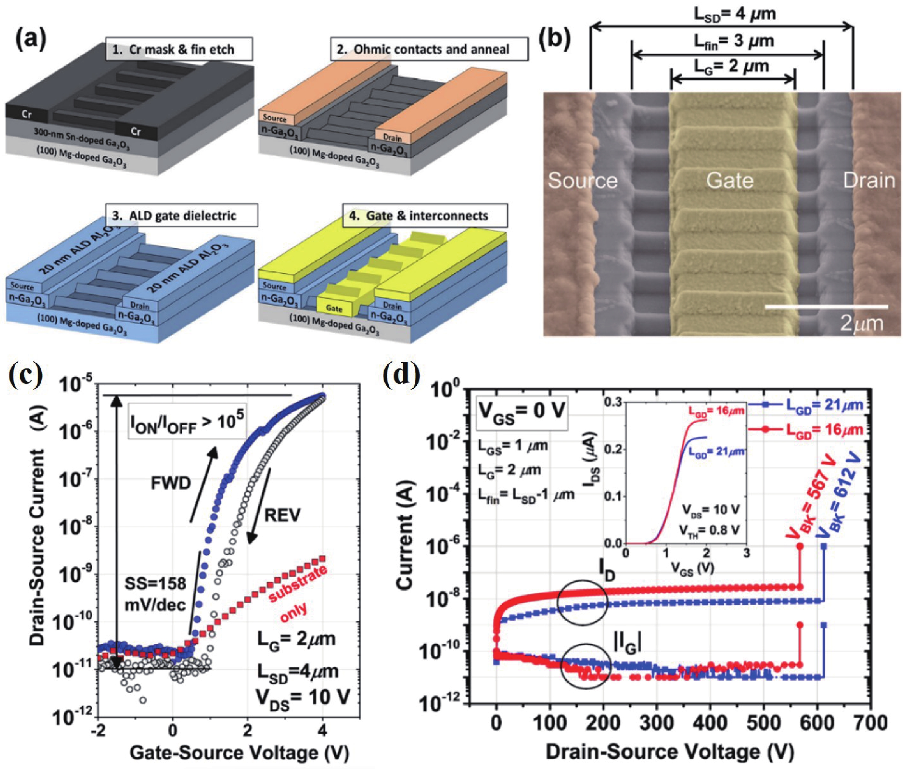
Chabak K D, Moser N, Green A J, et al. Enhancement-mode Ga 2O 3 wrap-gate fin field-effect transistors on native (100) β-Ga 2O 3 substrate with high breakdown voltage. Appl Phys Lett, 2016, 109, 213501 doi: 10.1063/1.4967931 |
| [41] |
Hogan J E, Kaun S W, Ahmadi E, et al. Chlorine-based dry etching of β-Ga 2O 3. Semicond Sci Technol, 2016, 31, 065006 doi: 10.1088/0268-1242/31/6/065006 |
| [42] |
Dong H, Long S B, Sun H D, et al. Fast switching β-Ga 2O 3 power MOSFET with a trench-gate structure. IEEE Electron Device Lett, 2019, 40, 1385 doi: 10.1109/LED.2019.2926202 |
| [43] |
Green A J, Chabak K D, Baldini M, et al. β-Ga 2O 3 MOSFETs for radio frequency operation. IEEE Electron Device Lett, 2017, 38, 790 doi: 10.1109/LED.2017.2694805 |
| [44] |
Do H B, Phan-Gia A V, Nguyen V Q, et al. Optimization of normally-off β-Ga 2O 3 MOSFET with high I on and BFOM: A TCAD study. AIP Adv, 2022, 12, 065024 doi: 10.1063/5.0094418 |
| [45] |
Do H B, Luc Q H, Ha M T H, et al. Investigation of Mo/Ti/AlN/HfO 2 high-k metal gate stack for low power consumption InGaAs NMOS device application. IEEE Electron Device Lett, 2017, 38, 552 doi: 10.1109/LED.2017.2688389 |
| [46] |
Wong M H, Nakata Y, Kuramata A, et al. Enhancement-mode Ga 2O 3 MOSFETs with Si-ion-implanted source and drain. Appl Phys Express, 2017, 10, 041101 doi: 10.7567/APEX.10.041101 |
| [47] |
Guo L L, Luan S Z, Zhang H P, et al. Analytical model and structure of the multilayer enhancement-mode β-Ga 2O 3 planar MOSFETs. IEEE Trans Electron Devices, 2022, 69, 682 doi: 10.1109/TED.2021.3137097 |
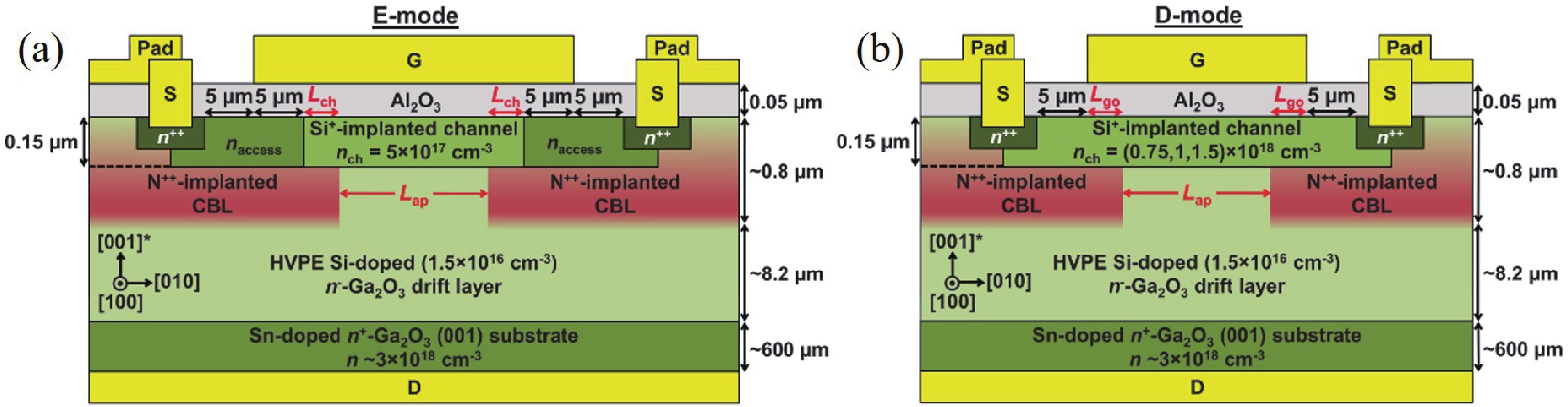
| [48] |
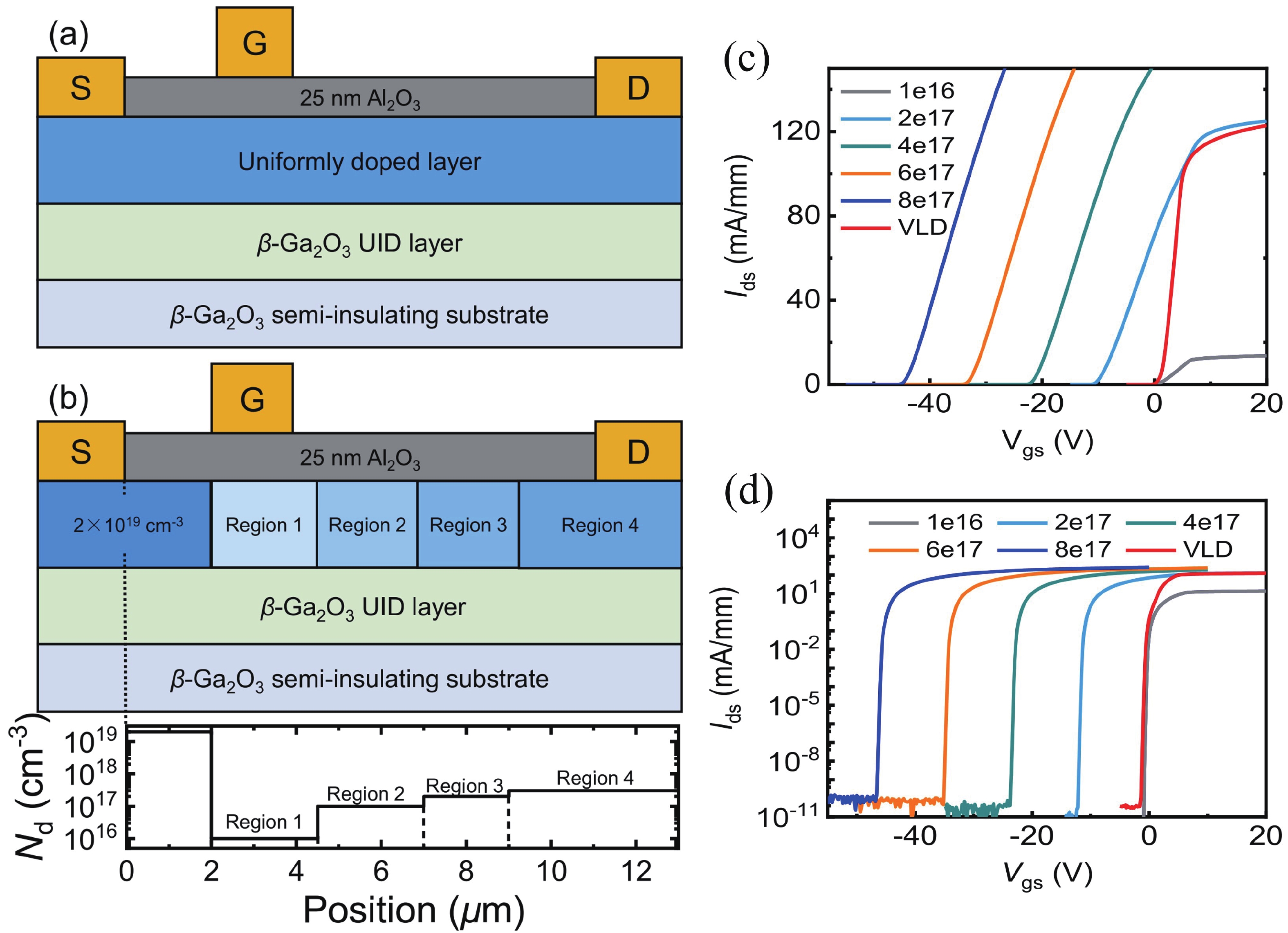
Zhou X Z, Liu Q, Xu G W, et al. Realizing high-performance β-Ga 2O 3 MOSFET by using variation of lateral doping: A TCAD study. IEEE Trans Electron Devices, 2021, 68, 1501 doi: 10.1109/TED.2021.3056326 |
| [49] |
Stengl R, Gosele U. Variation of lateral doping - A new concept to avoid high voltage breakdown of planar junctions. 1985 International Electron Devices Meeting, 2005, 154 doi: 10.1109/IEDM.1985.190917 |
| [50] |
Lv Y J, Zhou X Y, Long S B, et al. Enhancement-mode β-Ga 2O 3 metal-oxide-semiconductor field-effect transistor with high breakdown voltage over 3000 V realized by oxygen annealing. Phys Status Solidi RRL, 2020, 14, 1900586 doi: 10.1002/pssr.201900586 |
| [51] |
Ghosh S, Baral M, Kamparath R, et al. Investigations on band commutativity at all oxide p-type NiO/n-type β-Ga 2O 3 heterojunction using photoelectron spectroscopy. Appl Phys Lett, 2019, 115, 251603 doi: 10.1063/1.5126150 |
| [52] |
Lu X, Zhou X D, Jiang H X, et al. 1-kV sputtered p-NiO/n-Ga 2O 3 heterojunction diodes with an ultra-low leakage current below 1 μA/cm 2. IEEE Electron Device Lett, 2020, 41, 449 doi: 10.1109/LED.2020.2967418 |
| [53] |
Gong H H, Chen X H, Xu Y, et al. A 1.86-kV double-layered NiO/ β-Ga 2O 3 vertical p–n heterojunction diode. Appl Phys Lett, 2020, 117, 022104 doi: 10.1063/5.0010052 |
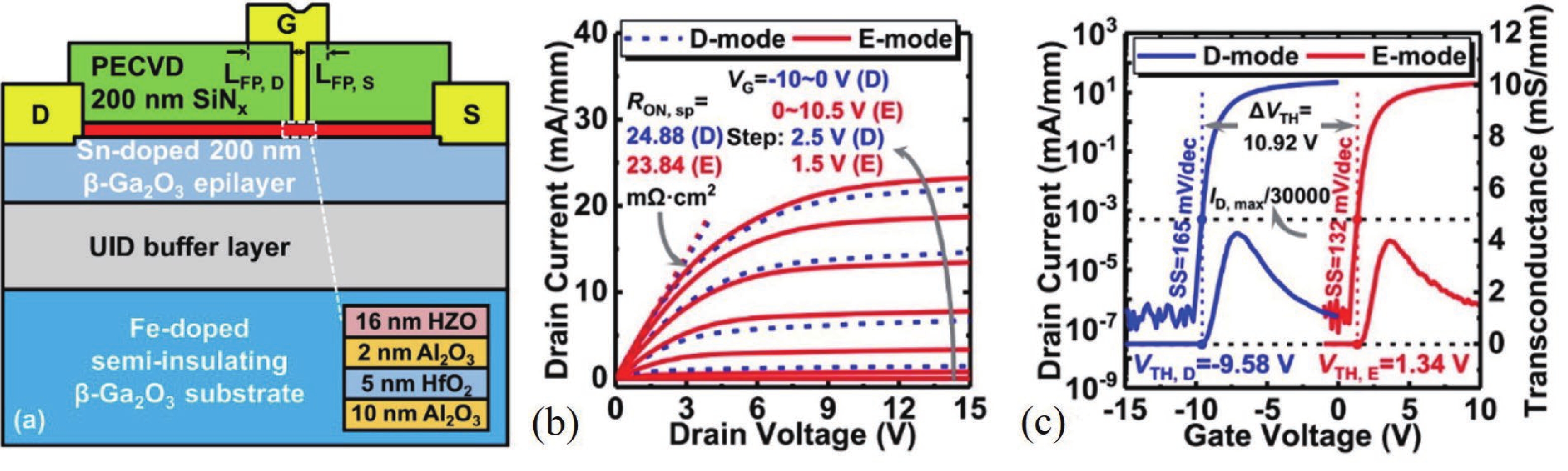
| [54] |
Wang C L, Gong H H, Lei W N, et al. Demonstration of the p-NiO x/n-Ga 2O 3 heterojunction gate FETs and diodes with BV 2/R on, sp figures of merit of 0.39 GW/cm 2 and 1.38 GW/cm 2. IEEE Electron Device Lett, 2021, 42, 485 doi: 10.1109/LED.2021.3062851 |
| [55] |
Lei W N, Dang K, Zhou H, et al. Proposal and simulation of Ga 2O 3 MOSFET with PN heterojunction structure for high-performance E-mode operation. IEEE Trans Electron Devices, 2022, 69, 3617 doi: 10.1109/TED.2022.3172919 |
| [56] |
Murakami H, Nomura K, Goto K, et al. Homoepitaxial growth of β-Ga 2O 3 layers by halide vapor phase epitaxy. Appl Phys Express, 2015, 8, 015503 doi: 10.7567/APEX.8.015503 |
| [57] |
Wong M H, Goto K, Murakami H, et al. Current aperture vertical β-Ga 2O 3 MOSFETs fabricated by N- and Si-ion implantation doping. IEEE Electron Device Lett, 2019, 40, 431 doi: 10.1109/LED.2018.2884542 |
| [58] |
Wong M H, Murakami H, Kumagai Y, et al. Enhancement-mode β-Ga 2O 3 current aperture vertical MOSFETs with N-ion-implanted blocker. IEEE Electron Device Lett, 2020, 41, 296 doi: 10.1109/LED.2019.2962657 |
| [59] |
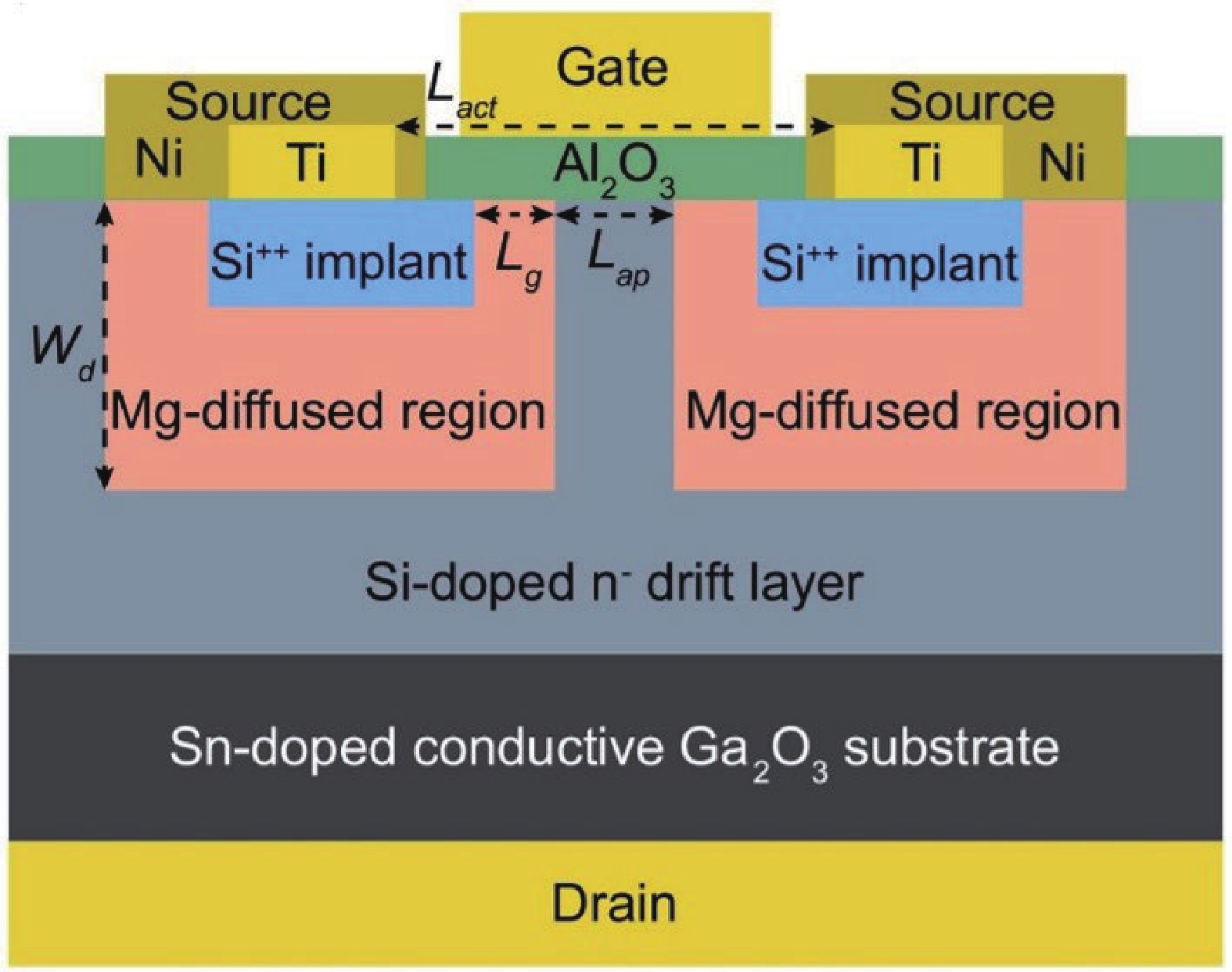
Zeng K, Soman R, Bian Z L, et al. Vertical Ga 2O 3 MOSFET with magnesium diffused current blocking layer. IEEE Electron Device Lett, 2022, 43, 1527 doi: 10.1109/LED.2022.3196035 |
| [60] |
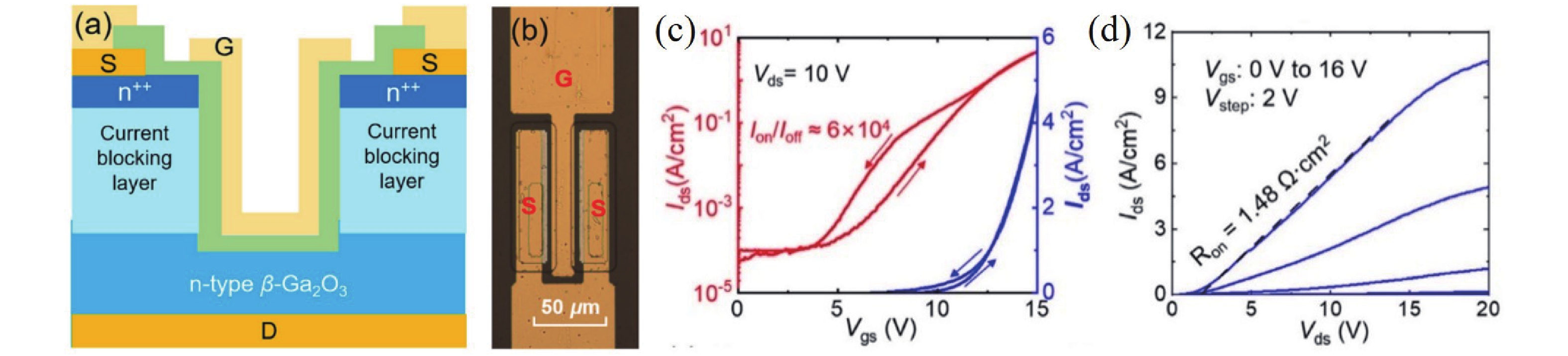
Zhou X Z, Ma Y J, Xu G W, et al. Enhancement-mode β-Ga 2O 3 U-shaped gate trench vertical MOSFET realized by oxygen annealing. Appl Phys Lett, 2022, 121, 223501 doi: 10.1063/5.0130292 |
| [61] |
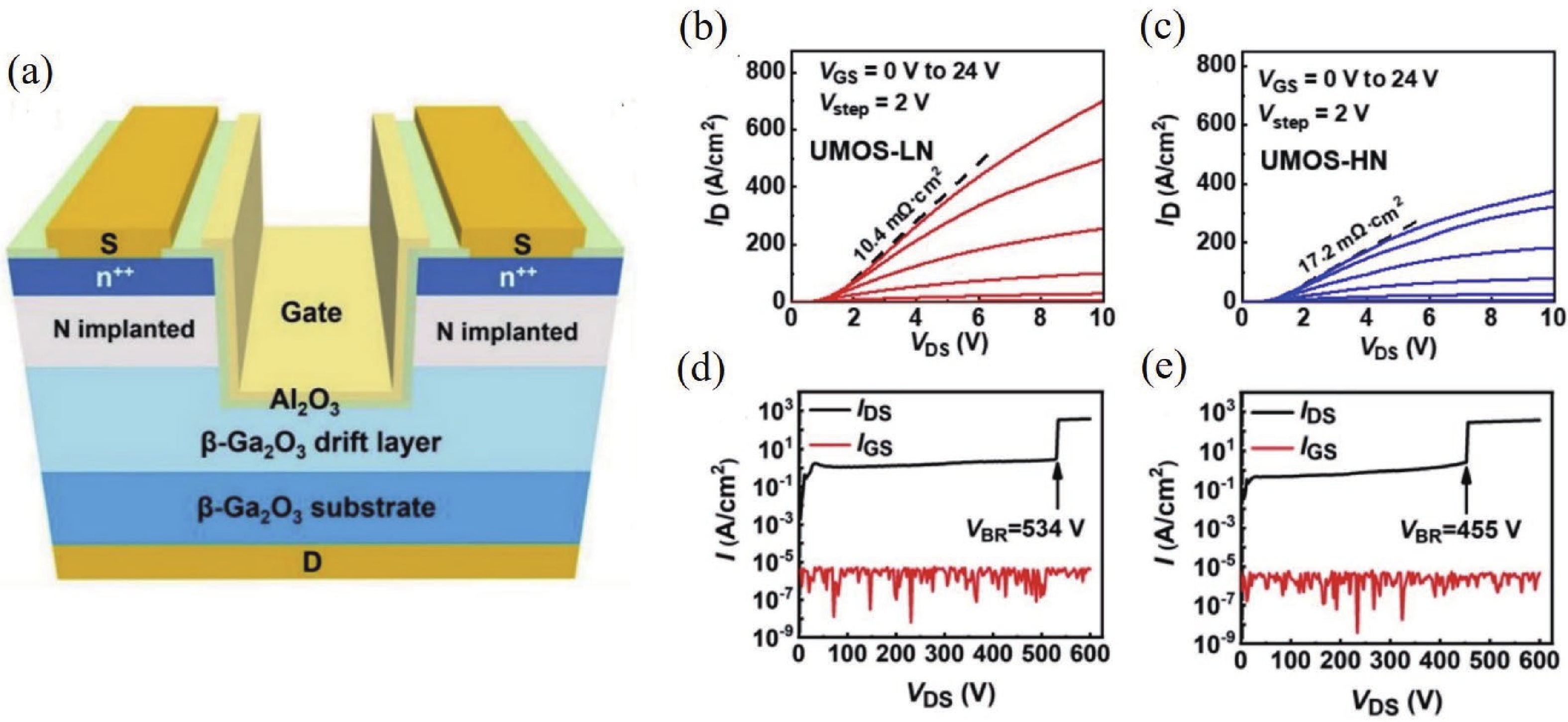
Ma Y, Zhou X, Tang W, et al. 702.3 A∙ cm –2/10.4 mΩ∙cm 2 vertical β-Ga 2O 3 U-shape trench gate MOSFET with N-ion implantation. IEEE Electron Device Lett, 2023, 44, 384 doi: 10.1109/LED.2023.3235777 |
| [62] |
Hu Z Y, Nomoto K, Li W S, et al. Enhancement-mode Ga 2O 3 vertical transistors with breakdown voltage >1 kV. IEEE Electron Device Lett, 2018, 39, 869 doi: 10.1109/LED.2018.2830184 |
| [63] |
Hu Z Y, Nomoto K, Li W S, et al. 1.6 kV vertical Ga 2O 3 FinFETs with source-connected field plates and normally-off operation. 2019 31st International Symposium on Power Semiconductor Devices and ICs (ISPSD), 2019, 483 doi: 10.1109/ISPSD.2019.8757633 |
| [64] |
Li W, Nomoto K, Hu Z, et al. Single and multi-fin normally-off Ga 2O 3 vertical transistors with a breakdown voltage over 2.6 kV. 2019 IEEE International Electron Devices Meeting (IEDM), 2020, 12.4.1 doi: 10.1109/IEDM19573.2019.8993526 |
| [65] |
Zeng K, Vaidya A, Singisetti U. 1.85 kV breakdown voltage in lateral field-plated Ga 2O 3 MOSFETs. IEEE Electron Device Lett, 2018, 39, 1385 doi: 10.1109/LED.2018.2859049 |
| [66] |
Mun J K, Cho K, Chang W, et al. 2.32 kV breakdown voltage lateral β-Ga 2O 3 MOSFETs with source-connected field plate. ECS J Solid State Sci Technol, 2019, 8, Q3079 doi: 10.1149/2.0151907jss |
| [67] |
Wang Y B, Gong H H, Jia X L, et al. Demonstration of β-Ga 2O 3 superjunction-equivalent MOSFETs. IEEE Trans Electron Devices, 2022, 69, 2203 doi: 10.1109/TED.2022.3152464 |
| [68] |
Deboy G, Marz N, Stengl J P, et al. A new generation of high voltage MOSFETs breaks the limit line of silicon. International Electron Devices Meeting, 1998, 683 doi: 10.1109/IEDM.1998.746448 |
| [69] |
Kim J, Kim K. A novel 4H-SiC super junction UMOSFET with heterojunction diode for enhanced reverse recovery characteristics. 2020 International Conference on Electronics, Information, and Communication (ICEIC), 2020, 1 doi: 10.1109/ICEIC49074.2020.9051221 |
| [70] |
Nakajima A, Sumida Y, Dhyani M H, et al. GaN-based super heterojunction field effect transistors using the polarization junction concept. IEEE Electron Device Lett, 2011, 32, 542 doi: 10.1109/LED.2011.2105242 |
| [71] |
Kim S H, Shoemaker D, Chatterjee B, et al. Thermally-aware layout design of β-Ga 2O 3 lateral MOSFETs. IEEE Trans Electron Devices, 2022, 69, 1251 doi: 10.1109/TED.2022.3143779 |
| [72] |
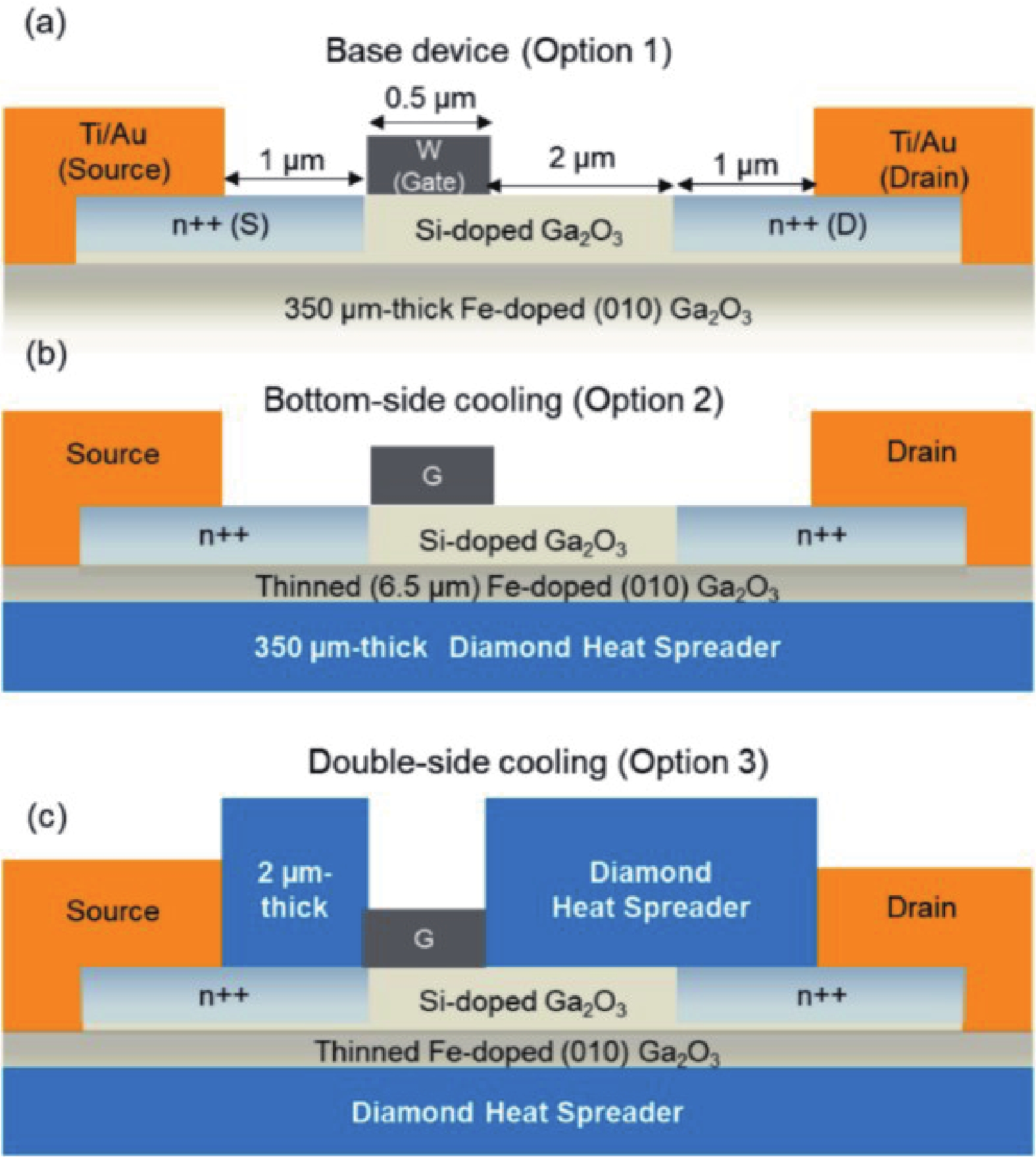
Kim S H, Spencer lundh J, Shoemaker D, et al. Device-level transient cooling of β-Ga 2O 3 MOSFETs. 2022 21st IEEE Intersociety Conference on Thermal and Thermomechanical Phenomena in Electronic Systems (iTherm), 2022, 1 doi: 10.1109/iTherm54085.2022.9899595 |


 DownLoad:


 Botong Li:got his BS degree from Jilin University in 2021. Now he is a master student at Suzhou Institute of Nano-Tech and Nano-Bionics, Chinese Academy of Sciences, under the supervision of Prof. Baoshun Zhang. His research focuses on the epitaxial growth and device fabrication of Ga2O3
 Baoshun Zhang:received his BS degree from Changchun University of Science and Technology in 1994 and PhD degree from the Institute of Semiconductors, Chinese Academy of Sciences in 2003. Then he joined in Hong Kong University of Science and Technology. Currently, he is a researcher at Suzhou Institute of Nano-Tech and Nano-Bionics, Chinese Academy of Sciences, and his research interests include semiconductor material growth and device technology research


