


Fig. 1.
(Color online) (a) Device schematic and (b) I–V characteristics of the sol-gel NiO/β-Ga2O3 heterojunction diode. Reproduced from Ref. [26]. Copyright 2016, The Japan Society of Applied Physics.
REVIEWS
Xing Lu, Yuxin Deng, Yanli Pei, Zimin Chen and Gang Wang
Corresponding author: Gang Wang, stswangg@mail.sysu.edu.cn
Abstract: Beta gallium oxide (β-Ga2O3) has attracted significant attention for applications in power electronics due to its ultra-wide bandgap of ~ 4.8 eV and the large critical electric field of 8 MV/cm. These properties yield a high Baliga’s figures of merit (BFOM) of more than 3000. Though β-Ga2O3 possesses superior material properties, the lack of p-type doping is the main obstacle that hinders the development of β-Ga2O3-based power devices for commercial use. Constructing heterojunctions by employing other p-type materials has been proven to be a feasible solution to this issue. Nickel oxide (NiO) is the most promising candidate due to its wide band gap of 3.6–4.0 eV. So far, remarkable progress has been made in NiO/β-Ga2O3 heterojunction power devices. This review aims to summarize recent advances in the construction, characterization, and device performance of the NiO/β-Ga2O3 heterojunction power devices. The crystallinity, band structure, and carrier transport property of the sputtered NiO/β-Ga2O3 heterojunctions are discussed. Various device architectures, including the NiO/β-Ga2O3 heterojunction pn diodes (HJDs), junction barrier Schottky (JBS) diodes, and junction field effect transistors (JFET), as well as the edge terminations and super-junctions based on the NiO/β-Ga2O3 heterojunction, are described.
Key words: gallium oxide (Ga2O3), nickel oxide (NiO), heterojunction, power devices
| [1] |
She X, Huang A Q, Lucía Ó, et al. Review of silicon carbide power devices and their applications. IEEE Trans Ind Electron, 2017, 64, 8193 doi: 10.1109/TIE.2017.2652401
|
| [2] |
Jones E A, Wang F F, Costinett D. Review of commercial GaN power devices and GaN-based converter design challenges. IEEE J Emerg Sel Top Power Electron, 2016, 4, 707 doi: 10.1109/JESTPE.2016.2582685
|
| [3] |
Saikumar A K, Nehate S D, Sundaram K B. Review—RF sputtered films of Ga2O3. ECS J Solid State Sci Technol, 2019, 8, Q3064 doi: 10.1149/2.0141907jss
|
| [4] |
Pearton S J, Yang J C, Cary P H, et al. A review of Ga2O3 materials, processing, and devices. Appl Phys Rev, 2018, 5, 011301 doi: 10.1063/1.5006941
|
| [5] |
Zhou H, Zhang J C, Zhang C F, et al. A review of the most recent progresses of state-of-art gallium oxide power devices. J Semicond, 2019, 40, 011803 doi: 10.1088/1674-4926/40/1/011803
|
| [6] |
Yoshioka S, Hayashi H, Kuwabara A, et al. Structures and energetics of Ga2O3 polymorphs. J Phys: Condens Matter, 2007, 19, 346211 doi: 10.1088/0953-8984/19/34/346211
|
| [7] |
Víllora E G, Shimamura K, Yoshikawa Y, et al. Large-size β-Ga2O3 single crystals and wafers. J Cryst Growth, 2004, 270, 420 doi: 10.1016/j.jcrysgro.2004.06.027
|
| [8] |
Kuramata A, Koshi K, Watanabe S, et al. High-quality β-Ga2O3 single crystals grown by edge-defined film-fed growth. Jpn J Appl Phys, 2016, 55, 1202A2 doi: 10.7567/JJAP.55.1202A2
|
| [9] |
Alema F, Zhang Y W, Osinsky A, et al. Low temperature electron mobility exceeding 104 cm2/V s in MOCVD grown β-Ga2O3. APL Mater, 2019, 7, 121110 doi: 10.1063/1.5132954
|
| [10] |
Zhang Y W, Alema F, Mauze A, et al. MOCVD grown epitaxial β-Ga2O3 thin film with an electron mobility of 176 cm2/V s at room temperature. APL Mater, 2018, 7, 022506 doi: 10.1063/1.5058059
|
| [11] |
Chen Y P, Xia X C, Liang H W, et al. Growth pressure controlled nucleation epitaxy of pure phase ε- and β-Ga2O3 films on Al2O3 via metal–organic chemical vapor deposition. Cryst Growth Des, 2018, 18, 1147 doi: 10.1021/acs.cgd.7b01576
|
| [12] |
Kukushkin S A, Nikolaev V I, Osipov A V, et al. Epitaxial gallium oxide on a SiC/Si substrate. Phys Solid State, 2016, 58, 1876 doi: 10.1134/S1063783416090201
|
| [13] |
Wei H L, Chen Z W, Wu Z P, et al. Epitaxial growth and characterization of CuGa2O4 films by laser molecular beam epitaxy. AIP Adv, 2017, 7, 115216 doi: 10.1063/1.5009032
|
| [14] |
Sasaki K, Higashiwaki M, Kuramata A, et al. MBE grown Ga2O3 and its power device applications. J Cryst Growth, 2013, 378, 591 doi: 10.1016/j.jcrysgro.2013.02.015
|
| [15] |
Joishi C, Rafique S, Xia Z B, et al. Low-pressure CVD-grown β-Ga2O3 bevel-field-plated Schottky barrier diodes. Appl Phys Express, 2018, 11, 031101 doi: 10.7567/APEX.11.031101
|
| [16] |
Baldini M, Albrecht M, Fiedler A, et al. Si- and Sn-doped homoepitaxial β-Ga2O3 layers grown by MOVPE on (010)-oriented substrates. ECS J Solid State Sci Technol, 2016, 6, Q3040 doi: 10.1149/2.0081702jss
|
| [17] |
Varley J B, Janotti A, Franchini C, et al. Role of self-trapping in luminescence and p-type conductivity of wide-band-gap oxides. Phys Rev B, 2012, 85, 081109 doi: 10.1103/PhysRevB.85.081109
|
| [18] |
Lyons J L. A survey of acceptor dopants for β. Semicond Sci Technol, 2018, 33, 05LT02 doi: 10.1088/1361-6641/aaba98
|
| [19] |
Yang J C, Xian M H, Carey P, et al. Vertical geometry 33.2 A, 4.8 MW cm2 Ga2O3 field-plated Schottky rectifier arrays. Appl Phys Lett, 2019, 114, 232106 doi: 10.1063/1.5100256
|
| [20] |
Zhou H, Yan Q L, Zhang J C, et al. High-performance vertical β-Ga2O3 Schottky barrier diode with implanted edge termination. IEEE Electron Device Lett, 2019, 40, 1788 doi: 10.1109/LED.2019.2939788
|
| [21] |
Li W S, Nomoto K, Hu Z Y, et al. Field-plated Ga2O3 trench Schottky barrier diodes with a BV2/Ron, sp of up to 0.95 GW/cm2. IEEE Electron Device Lett, 2020, 41, 107 doi: 10.1109/LED.2019.2953559
|
| [22] |
Jian Z A, Mohanty S, Ahmadi E. Switching performance analysis of 3.5 kV Ga2O3 power FinFETs. IEEE Trans Electron Devices, 2021, 68, 672 doi: 10.1109/TED.2020.3043988
|
| [23] |
Nakagomi S, Hiratsuka K, Kakuda Y, et al. Beta-gallium oxide/SiC heterojunction diodes with high rectification ratios. ECS J Solid State Sci Technol, 2016, 6, Q3030 doi: 10.1149/2.0061702jss
|
| [24] |
Zhang Y C, Li Y F, Wang Z Z, et al. Investigation of β-Ga2O3 films and β-Ga2O3/GaN heterostructures grown by metal organic chemical vapor deposition. Sci China Phys Mech Astron, 2020, 63, 117311 doi: 10.1007/s11433-019-1546-3
|
| [25] |
Wang Y G, Gong H H, Lv Y J, et al. 2.41 kV vertical P-NiO/n-Ga2O3 heterojunction diodes with a record Baliga’s figure-of-merit of 5.18 GW/cm2. IEEE Trans Power Electron, 2022, 37, 3743 doi: 10.1109/TPEL.2021.3123940
|
| [26] |
Kokubun Y, Kubo S, Nakagomi S. All-oxide p–n heterojunction diodes comprising p-type NiO and n-type β-Ga2O3. Appl Phys Express, 2016, 9, 091101 doi: 10.7567/APEX.9.091101
|
| [27] |
Lu X, Zhou X D, Jiang H X, et al. 1-kV sputtered p-NiO/n-Ga2O3 heterojunction diodes with an ultra-low leakage current below 1 μA/cm2. IEEE Electron Device Lett, 2020, 41, 449 doi: 10.1109/LED.2020.2967418
|
| [28] |
Watahiki T, Yuda Y, Furukawa A, et al. Heterojunction p-Cu2O/n-Ga2O3 diode with high breakdown voltage. Appl Phys Lett, 2017, 111, 222104 doi: 10.1063/1.4998311
|
| [29] |
Budde M, Splith D, Mazzolini P, et al. SnO/β-Ga2O3 vertical pn heterojunction diodes. Appl Phys Lett, 2020, 117, 252106 doi: 10.1063/5.0031442
|
| [30] |
Gallagher J C, Koehler A D, Tadjer M J, et al. Demonstration of CuI as a P–N heterojunction to β. Appl Phys Express, 2019, 12, 104005 doi: 10.7567/1882-0786/ab420e
|
| [31] |
Chen H L, Lu Y M, Hwang W S. Characterization of sputtered NiO thin films. Surf Coat Technol, 2005, 198, 138 doi: 10.1016/j.surfcoat.2004.10.032
|
| [32] |
Lv Y J, Wang Y G, Fu X C, et al. Demonstration of β-Ga2O3 junction barrier Schottky diodes with a Baliga’s figure of merit of 0.85 GW/cm2 or a 5A/700 V handling capabilities. IEEE Trans Power Electron, 2021, 36, 6179 doi: 10.1109/TPEL.2020.3036442
|
| [33] |
Wang C L, Gong H H, Lei W N, et al. Demonstration of the p-NiOx/n-Ga2O3 heterojunction gate FETs and diodes with BV2/Ron, sp figures of merit of 0.39 GW/cm2 and 1.38 GW/cm2. IEEE Electron Device Lett, 2021, 42, 485 doi: 10.1109/LED.2021.3062851
|
| [34] |
Yan Q L, Gong H H, Zhou H, et al. Low density of interface trap states and temperature dependence study of Ga2O3 Schottky barrier diode with p-NiOx termination. Appl Phys Lett, 2022, 120, 092106 doi: 10.1063/5.0082377
|
| [35] |
Wang Y B, Gong H H, Jia X L, et al. Demonstration of β-Ga2O3 superjunction-equivalent MOSFETs. IEEE Trans Electron Devices, 2022, 69, 2203 doi: 10.1109/TED.2022.3152464
|
| [36] |
Wang Y, Qin Q Z. A nanocrystalline NiO thin-film electrode prepared by pulsed laser ablation for Li-ion batteries. J Electrochem Soc, 2002, 149, A873 doi: 10.1149/1.1481715
|
| [37] |
Jlassi M, Sta I, Hajji M, et al. Optical and electrical properties of nickel oxide thin films synthesized by sol–gel spin coating. Mater Sci Semicond Process, 2014, 21, 7 doi: 10.1016/j.mssp.2014.01.018
|
| [38] |
Park J H, Seo J, Park S, et al. Efficient CH3NH3PbI3 perovskite solar cells employing nanostructured p-type NiO electrode formed by a pulsed laser deposition. Adv Mater, 2015, 27, 4013 doi: 10.1002/adma.201500523
|
| [39] |
Hotový I, Búc D, Haščík Š, et al. Characterization of NiO thin films deposited by reactive sputtering. Vacuum, 1998, 50, 41 doi: 10.1016/S0042-207X(98)00011-6
|
| [40] |
Budde M, Remmele T, Tschammer C, et al. Plasma-assisted molecular beam epitaxy of NiO on GaN(00.1). J Appl Phys, 2020, 127, 015306 doi: 10.1063/1.5129881
|
| [41] |
Tadjer M J, Luna L E, Cleveland E, et al. Fabrication and characterization of β-Ga2O3 heterojunction rectifiers. ECS Trans, 2018, 85, 21 doi: 10.1149/08507.0021ecst
|
| [42] |
Hajakbari F. Characterization of nanocrystalline nickel oxide thin films prepared at different thermal oxidation temperatures. J Nanostruct Chem, 2020, 10, 97 doi: 10.1007/s40097-020-00332-2
|
| [43] |
Pintor-Monroy M I, Barrera D, Murillo-Borjas B L, et al. Tunable electrical and optical properties of nickel oxide (NiOx) thin films for fully transparent NiOx-Ga2O3 p-n junction diodes. ACS Appl Mater Interfaces, 2018, 10, 38159 doi: 10.1021/acsami.8b08095
|
| [44] |
Schlupp P, Splith D, von Wenckstern H, et al. Electrical properties of vertical p-NiO/n-Ga2O3 and p-ZnCo2O4/n-Ga2O3 pn-heterodiodes. Phys Status Solidi A, 2019, 216, 1800729 doi: 10.1002/pssa.201800729
|
| [45] |
Zhang J Y, Han S B, Cui M Y, et al. Fabrication and interfacial electronic structure of wide bandgap NiO and Ga2O3 p–n heterojunction. ACS Appl Electron Mater, 2020, 2, 456 doi: 10.1021/acsaelm.9b00704
|
| [46] |
Li K H, Alfaraj N, Kang C H, et al. Deep-ultraviolet photodetection using single-crystalline β-Ga2O3/NiO heterojunctions. ACS Appl Mater Interfaces, 2019, 11, 35095 doi: 10.1021/acsami.9b10626
|
| [47] |
Deng Y X, Yang Z Q, Xu T L, et al. Band alignment and electrical properties of NiO/β-Ga2O3 heterojunctions with different β-Ga2O3 orientations. Appl Surf Sci, 2023, 622, 156917 doi: 10.1016/j.apsusc.2023.156917
|
| [48] |
Luo H X, Zhou X D, Chen Z M, et al. Fabrication and characterization of high-voltage NiO/β-Ga2O3 heterojunction power diodes. IEEE Trans Electron Devices, 2021, 68, 3991 doi: 10.1109/TED.2021.3091548
|
| [49] |
Liao C, Lu X, Xu T L, et al. Optimization of NiO/β-Ga2O3 heterojunction diodes for high-power application. IEEE Trans Electron Devices, 2022, 69, 5722 doi: 10.1109/TED.2022.3200642
|
| [50] |
Gong H H, Chen X H, Xu Y, et al. Band alignment and interface recombination in NiO/β-Ga2O3 type-II p-n heterojunctions. IEEE Trans Electron Devices, 2020, 67, 3341 doi: 10.1109/TED.2020.3001249
|
| [51] |
Guo Z, Verma A, Wu X F, et al. Anisotropic thermal conductivity in single crystal β-gallium oxide. Appl Phys Lett, 2015, 106, 111909 doi: 10.1063/1.4916078
|
| [52] |
Wong M H, Sasaki K, Kuramata A, et al. Electron channel mobility in silicon-doped Ga2O3 MOSFETs with a resistive buffer layer. Jpn J Appl Phys, 2016, 55, 1202B9 doi: 10.7567/JJAP.55.1202B9
|
| [53] |
Jang S, Jung S, Beers K, et al. A comparative study of wet etching and contacts on ( $ \bar{2}01$) and (010) oriented β-Ga2O3. J Alloys Compd, 2018, 731, 118 doi: 10.1016/j.jallcom.2017.09.336
|
| [54] |
Zhang K, Xu Z W, Zhao J L, et al. Anisotropies of angle-resolved polarized Raman response identifying in low miller index β-Ga2O3 single crystal. Appl Surf Sci, 2022, 581, 152426 doi: 10.1016/j.apsusc.2022.152426
|
| [55] |
Yatskiv R, Tiagulskyi S, Grym J. Influence of crystallographic orientation on Schottky barrier formation in gallium oxide. J Electron Mater, 2020, 49, 5133 doi: 10.1007/s11664-020-07996-0
|
| [56] |
Fu H Q, Chen H, Huang X Q, et al. A comparative study on the electrical properties of vertical ( $\bar{2}01 $) and (010) β-Ga2O3 Schottky barrier diodes on EFG single-crystal substrates. IEEE Trans Electron Devices, 2018, 65, 3507 doi: 10.1109/TED.2018.2841904
|
| [57] |
Xia X Y, Li J S, Chiang C C, et al. Annealing temperature dependence of band alignment of NiO/β-Ga2O3. J Phys D: Appl Phys, 2022, 55, 385105 doi: 10.1088/1361-6463/ac7e84
|
| [58] |
Wang Z P, Gong H H, Meng C X, et al. Majority and minority carrier traps in NiO/β-Ga2O3 p-n heterojunction diode. IEEE Trans Electron Devices, 2022, 69, 981 doi: 10.1109/TED.2022.3143491
|
| [59] |
Grundmann M, Karsthof R, von Wenckstern H. Interface recombination current in type II heterostructure bipolar diodes. ACS Appl Mater Interfaces, 2014, 6, 14785 doi: 10.1021/am504454g
|
| [60] |
Riben A R, Feucht D L. Electrical transport in nGe-pGaAs heterojunctions. Int J Electron, 1966, 20, 583 doi: 10.1080/00207216608937891
|
| [61] |
Riben A R, Feucht D L. nGe–pGaAs heterojunctions. Solid State Electron, 1966, 9, 1055 doi: 10.1016/0038-1101(66)90129-8
|
| [62] |
Zhang J C, Dong P F, Dang K, et al. Ultra-wide bandgap semiconductor Ga2O3 power diodes. Nat Commun, 2022, 13, 3900 doi: 10.1038/s41467-022-31664-y
|
| [63] |
Wang Z P, Gong H H, Yu X X, et al. Trap-mediated bipolar charge transport in NiO/Ga2O3 p+-n heterojunction power diodes. Sci China Mater, 2022, 66, 1157 doi: 10.1007/s40843-022-2244-y
|
| [64] |
Zimmermann C, Frodason Y K, Barnard A W, et al. Ti- and Fe-related charge transition levels in β-Ga2O3. Appl Phys Lett, 2020, 116, 072101 doi: 10.1063/1.5139402
|
| [65] |
Ingebrigtsen M E, Varley J B, Kuznetsov A Y, et al. Iron and intrinsic deep level states in Ga2O3. Appl Phys Lett, 2018, 112, 042104 doi: 10.1063/1.5020134
|
| [66] |
Hao W B, He Q M, Zhou K, et al. Low defect density and small I − V curve hysteresis in NiO/β-Ga2O3 pn diode with a high PFOM of 0.65 GW/cm2. Appl Phys Lett, 2021, 118, 043501 doi: 10.1063/5.0038349
|
| [67] |
Gong H H, Yu X X, Xu Y, et al. Vertical field-plated NiO/Ga2O3 heterojunction power diodes. 2021 5th IEEE Electron Devices Technology & Manufacturing Conference (EDTM), 2021, 1 doi: 10.1109/EDTM50988.2021.9420914
|
| [68] |
Gong H H, Chen X H, Xu Y, et al. A 1.86-kV double-layered NiO/β-Ga2O3 vertical p–n heterojunction diode. Appl Phys Lett, 2020, 117, 022104 doi: 10.1063/5.0010052
|
| [69] |
Li J S, Chiang C C, Xia X Y, et al. Demonstration of 4.7 kV breakdown voltage in NiO/β-Ga2O3 vertical rectifiers. Appl Phys Lett, 2022, 121, 042105 doi: 10.1063/5.0097564
|
| [70] |
Zhou F, Gong H H, Wang Z P, et al. Over 1.8 GW/cm2 beveled-mesa NiO/β-Ga2O3 heterojunction diode with 800 V/10 A nanosecond switching capability. Appl Phys Lett, 2021, 119, 262103 doi: 10.1063/5.0071280
|
| [71] |
Gong H H, Yu X X, Xu Y, et al. β-Ga2O3 vertical heterojunction barrier Schottky diodes terminated with p-NiO field limiting rings. Appl Phys Lett, 2021, 118, 202102 doi: 10.1063/5.0050919
|
| [72] |
De Santi C, Fregolent M, Buffolo M, et al. Carrier capture kinetics, deep levels, and isolation properties of β-Ga2O3 Schottky-barrier diodes damaged by nitrogen implantation. Appl Phys Lett, 2020, 117, 262108 doi: 10.1063/5.0029295
|
| [73] |
Yan Q L, Gong H H, Zhang J C, et al. β-Ga2O3 hetero-junction barrier Schottky diode with reverse leakage current modulation and BV2/Ron,sp value of 0.93 GW/cm2. Appl Phys Lett, 2021, 118, 122102 doi: 10.1063/5.0044130
|
| [74] |
Polyakov A Y, Lee I H, Smirnov N B, et al. Defects at the surface of β-Ga2O3 produced by Ar plasma exposure. APL Mater, 2019, 7, 061102 doi: 10.1063/1.5109025
|
| [75] |
Alfieri G, Mihaila A, Godignon P, et al. Deep level study of chlorine-based dry etched β-Ga2O3. J Appl Phys, 2021, 130, 025701 doi: 10.1063/5.0050416
|
| [76] |
Lu X, Xu T L, Deng Y X, et al. Performance-enhanced NiO/β-Ga2O3 heterojunction diodes fabricated on an etched β-Ga2O3 surface. Appl Surf Sci, 2022, 597, 153587 doi: 10.1016/j.apsusc.2022.153587
|
| [77] |
Lv Y J, Zhou X Y, Long S B, et al. Lateral source field-plated β-Ga2O3 MOSFET with recorded breakdown voltage of 2360 V and low specific on-resistance of 560 mΩ cm2. Semicond Sci Technol, 2019, 34, 11LT02 doi: 10.1088/1361-6641/ab4214
|
| [78] |
Mun J K, Cho K, Chang W, et al. Editors' choice—2.32 kV breakdown voltage lateral β-Ga2O3 MOSFETs with source-connected field plate. ECS J Solid State Sci Technol, 2019, 8, Q3079 doi: 10.1149/2.0151907jss
|
| [79] |
Tetzner K, Bahat Treidel E, Hilt O, et al. Lateral 1.8 kV β-Ga2O3 MOSFET with 155 MW/cm2 power figure of merit. IEEE Electron Device Lett, 2019, 40, 1503 doi: 10.1109/LED.2019.2930189
|
| [80] |
Lv Y J, Liu H Y, Zhou X Y, et al. Lateral β-Ga2O3 MOSFETs with high power figure of merit of 277 MW/cm2. IEEE Electron Device Lett, 2020, 41, 537 doi: 10.1109/LED.2020.2974515
|
| [81] |
Zhou X Z, Liu Q, Hao W B, et al. Normally-off β-Ga2O3 power heterojunction field-effect-transistor realized by p-NiO and recessed-gate. 2022 IEEE 34th International Symposium on Power Semiconductor Devices and ICs (ISPSD), 2022, 101 doi: 10.1109/ISPSD49238.2022.9813678
|
| [82] |
Konishi K, Goto K, Murakami H, et al. 1-kV vertical Ga2O3 field-plated Schottky barrier diodes. Appl Phys Lett, 2017, 110, 103506 doi: 10.1063/1.4977857
|
| [83] |
Zhang Y N, Zhang J C, Feng Z Q, et al. Impact of implanted edge termination on vertical β-Ga2O3 Schottky barrier diodes under OFF-state stressing. IEEE Trans Electron Devices, 2020, 67, 3948 doi: 10.1109/TED.2020.3002327
|
| [84] |
Gao Y Y, Li A, Feng Q, et al. High-voltage β-Ga2O3 Schottky diode with argon-implanted edge termination. Nanoscale Res Lett, 2019, 14, 8 doi: 10.1186/s11671-018-2849-y
|
| [85] |
Wang Y G, Lv Y J, Long S B, et al. High-voltage (-201) β-Ga2O3 vertical Schottky barrier diode with thermally-oxidized termination. IEEE Electron Device Lett, 2020, 41, 131 doi: 10.1109/LED.2019.2956016
|
| [86] |
Hirao T, Onose H, Kan Y S, et al. Edge termination with enhanced field-limiting rings insensitive to surface charge for high-voltage SiC power devices. IEEE Trans Electron Devices, 2020, 67, 2850 doi: 10.1109/TED.2020.2992577
|
| [87] |
Fujihira T. Theory of semiconductor superjunction devices. Jpn J Appl Phys, 1997, 36, 6254 doi: 10.1143/JJAP.36.6254
|
| [88] |
Deboy G, Marz N, Stengl J P, et al. A new generation of high voltage MOSFETs breaks the limit line of silicon. International Electron Devices Meeting, 1998, 683 doi: 10.1109/IEDM.1998.746448
|
| [89] |
Lorenz L, Deboy G, Knapp A, et al. COOLMOS/sup TM/-a new milestone in high voltage power MOS. 11th International Symposium on Power Semiconductor Devices and ICs, 1999, 3 doi: 10.1109/ISPSD.1999.764028
|
| [90] |
Udrea F, Deboy G, Fujihira T. Superjunction power devices, history, development, and future prospects. IEEE Trans Electron Devices, 2017, 64, 713 doi: 10.1109/TED.2017.2658344
|
| [91] |
Nassif-Khalil S G, Salama C A T. Super-junction LDMOST on a silicon-on-sapphire substrate. IEEE Trans Electron Devices, 2003, 50, 1385 doi: 10.1109/TED.2003.813460
|
| [92] |
Duan B X, Cao Z, Yuan X, et al. New superjunction LDMOS breaking silicon limit by electric field modulation of buffered step doping. IEEE Electron Device Lett, 2015, 36, 47 doi: 10.1109/LED.2014.2366298
|
| [93] |
Xiao M, Zhang R Z, Dong D, et al. Design and simulation of GaN superjunction transistors with 2-DEG channels and fin channels. IEEE J Emerg Sel Top Power Electron, 2019, 7, 1475 doi: 10.1109/JESTPE.2019.2912978
|
| [94] |
Zhong X Q, Wang B Z, Wang J, et al. Experimental demonstration and analysis of a 1.35-kV 0.92-m Ω·cm2 SiC superjunction Schottky diode. IEEE Trans Electron Devices, 2018, 65, 1458 doi: 10.1109/TED.2018.2809475
|
| [95] |
Nakajima A, Sumida Y, Dhyani M H, et al. GaN-based super heterojunction field effect transistors using the polarization junction concept. IEEE Electron Device Lett, 2011, 32, 542 doi: 10.1109/LED.2011.2105242
|
| [96] |
Wang H, Napoli E, Udrea F. Breakdown voltage for superjunction power devices with charge imbalance: An analytical model valid for both punch through and non punch through devices. IEEE Trans Electron Devices, 2009, 56, 3175 doi: 10.1109/TED.2009.2032595
|


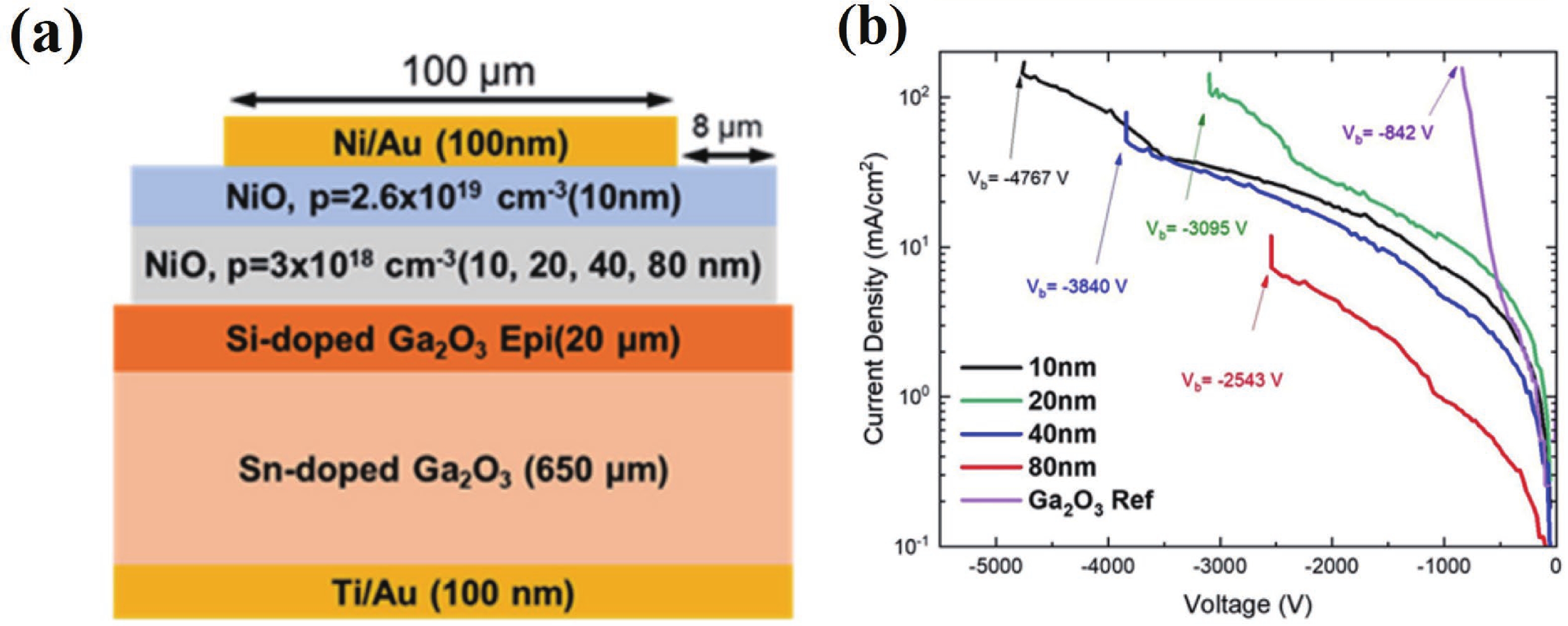
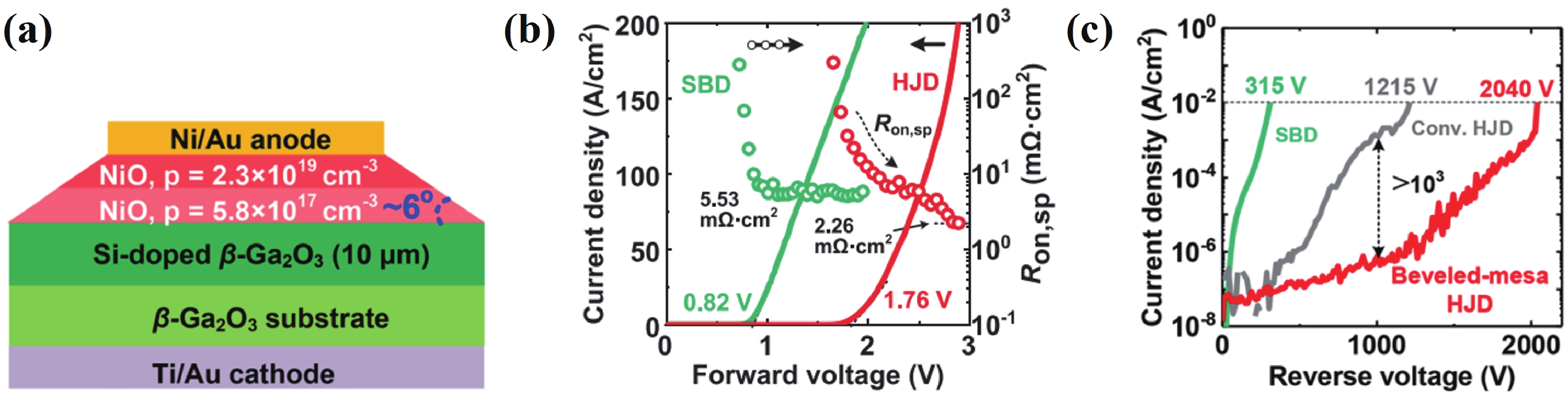
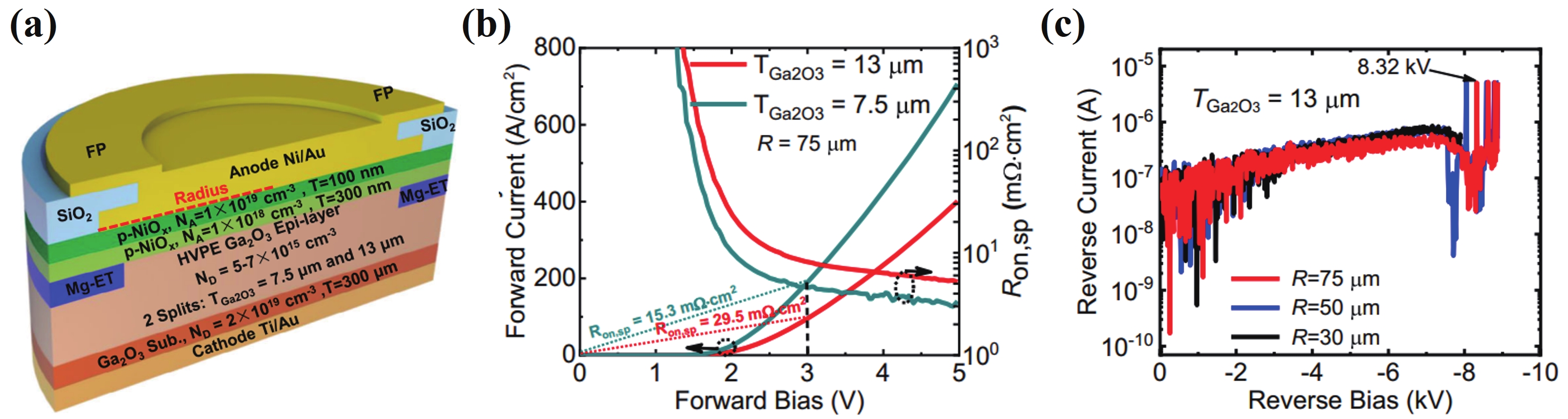

Table 1. Material properties of Ga2O3 and some competing semiconductors for power electronics.
| Material | Si | GaAs | 4H-SiC | GaN | Diamond | Ga2O3 |
| Band gap (eV) | 1.1 | 1.43 | 3.25 | 3.4 | 5.5 | 4.6–4.9 |
| Critical electric field (MV/cm) | 0.3 | 0.4 | 2.5 | 3.3 | 10 | 8 |
| Electron mobility (cm2/(V·s)) | 1480 | 8400 | 1000 | 1250 | 2000 | 300 |
| Dielectric constant | 11.8 | 12.9 | 9.7 | 9 | 5.5 | 10 |
| Baliga FOM (${\epsilon }{\mu }{{E} }_{{c} }^{3}$) | 1 | 14.7 | 317 | 846 | 24660 | >3000 |
 DownLoad: CSV
| [1] |
She X, Huang A Q, Lucía Ó, et al. Review of silicon carbide power devices and their applications. IEEE Trans Ind Electron, 2017, 64, 8193 doi: 10.1109/TIE.2017.2652401
|
| [2] |
Jones E A, Wang F F, Costinett D. Review of commercial GaN power devices and GaN-based converter design challenges. IEEE J Emerg Sel Top Power Electron, 2016, 4, 707 doi: 10.1109/JESTPE.2016.2582685
|
| [3] |
Saikumar A K, Nehate S D, Sundaram K B. Review—RF sputtered films of Ga2O3. ECS J Solid State Sci Technol, 2019, 8, Q3064 doi: 10.1149/2.0141907jss
|
| [4] |
Pearton S J, Yang J C, Cary P H, et al. A review of Ga2O3 materials, processing, and devices. Appl Phys Rev, 2018, 5, 011301 doi: 10.1063/1.5006941
|
| [5] |
Zhou H, Zhang J C, Zhang C F, et al. A review of the most recent progresses of state-of-art gallium oxide power devices. J Semicond, 2019, 40, 011803 doi: 10.1088/1674-4926/40/1/011803
|
| [6] |
Yoshioka S, Hayashi H, Kuwabara A, et al. Structures and energetics of Ga2O3 polymorphs. J Phys: Condens Matter, 2007, 19, 346211 doi: 10.1088/0953-8984/19/34/346211
|
| [7] |
Víllora E G, Shimamura K, Yoshikawa Y, et al. Large-size β-Ga2O3 single crystals and wafers. J Cryst Growth, 2004, 270, 420 doi: 10.1016/j.jcrysgro.2004.06.027
|
| [8] |
Kuramata A, Koshi K, Watanabe S, et al. High-quality β-Ga2O3 single crystals grown by edge-defined film-fed growth. Jpn J Appl Phys, 2016, 55, 1202A2 doi: 10.7567/JJAP.55.1202A2
|
| [9] |
Alema F, Zhang Y W, Osinsky A, et al. Low temperature electron mobility exceeding 104 cm2/V s in MOCVD grown β-Ga2O3. APL Mater, 2019, 7, 121110 doi: 10.1063/1.5132954
|
| [10] |
Zhang Y W, Alema F, Mauze A, et al. MOCVD grown epitaxial β-Ga2O3 thin film with an electron mobility of 176 cm2/V s at room temperature. APL Mater, 2018, 7, 022506 doi: 10.1063/1.5058059
|
| [11] |
Chen Y P, Xia X C, Liang H W, et al. Growth pressure controlled nucleation epitaxy of pure phase ε- and β-Ga2O3 films on Al2O3 via metal–organic chemical vapor deposition. Cryst Growth Des, 2018, 18, 1147 doi: 10.1021/acs.cgd.7b01576
|
| [12] |
Kukushkin S A, Nikolaev V I, Osipov A V, et al. Epitaxial gallium oxide on a SiC/Si substrate. Phys Solid State, 2016, 58, 1876 doi: 10.1134/S1063783416090201
|
| [13] |
Wei H L, Chen Z W, Wu Z P, et al. Epitaxial growth and characterization of CuGa2O4 films by laser molecular beam epitaxy. AIP Adv, 2017, 7, 115216 doi: 10.1063/1.5009032
|
| [14] |
Sasaki K, Higashiwaki M, Kuramata A, et al. MBE grown Ga2O3 and its power device applications. J Cryst Growth, 2013, 378, 591 doi: 10.1016/j.jcrysgro.2013.02.015
|
| [15] |
Joishi C, Rafique S, Xia Z B, et al. Low-pressure CVD-grown β-Ga2O3 bevel-field-plated Schottky barrier diodes. Appl Phys Express, 2018, 11, 031101 doi: 10.7567/APEX.11.031101
|
| [16] |
Baldini M, Albrecht M, Fiedler A, et al. Si- and Sn-doped homoepitaxial β-Ga2O3 layers grown by MOVPE on (010)-oriented substrates. ECS J Solid State Sci Technol, 2016, 6, Q3040 doi: 10.1149/2.0081702jss
|
| [17] |
Varley J B, Janotti A, Franchini C, et al. Role of self-trapping in luminescence and p-type conductivity of wide-band-gap oxides. Phys Rev B, 2012, 85, 081109 doi: 10.1103/PhysRevB.85.081109
|
| [18] |
Lyons J L. A survey of acceptor dopants for β. Semicond Sci Technol, 2018, 33, 05LT02 doi: 10.1088/1361-6641/aaba98
|
| [19] |
Yang J C, Xian M H, Carey P, et al. Vertical geometry 33.2 A, 4.8 MW cm2 Ga2O3 field-plated Schottky rectifier arrays. Appl Phys Lett, 2019, 114, 232106 doi: 10.1063/1.5100256
|
| [20] |
Zhou H, Yan Q L, Zhang J C, et al. High-performance vertical β-Ga2O3 Schottky barrier diode with implanted edge termination. IEEE Electron Device Lett, 2019, 40, 1788 doi: 10.1109/LED.2019.2939788
|
| [21] |
Li W S, Nomoto K, Hu Z Y, et al. Field-plated Ga2O3 trench Schottky barrier diodes with a BV2/Ron, sp of up to 0.95 GW/cm2. IEEE Electron Device Lett, 2020, 41, 107 doi: 10.1109/LED.2019.2953559
|
| [22] |
Jian Z A, Mohanty S, Ahmadi E. Switching performance analysis of 3.5 kV Ga2O3 power FinFETs. IEEE Trans Electron Devices, 2021, 68, 672 doi: 10.1109/TED.2020.3043988
|
| [23] |
Nakagomi S, Hiratsuka K, Kakuda Y, et al. Beta-gallium oxide/SiC heterojunction diodes with high rectification ratios. ECS J Solid State Sci Technol, 2016, 6, Q3030 doi: 10.1149/2.0061702jss
|
| [24] |
Zhang Y C, Li Y F, Wang Z Z, et al. Investigation of β-Ga2O3 films and β-Ga2O3/GaN heterostructures grown by metal organic chemical vapor deposition. Sci China Phys Mech Astron, 2020, 63, 117311 doi: 10.1007/s11433-019-1546-3
|
| [25] |
Wang Y G, Gong H H, Lv Y J, et al. 2.41 kV vertical P-NiO/n-Ga2O3 heterojunction diodes with a record Baliga’s figure-of-merit of 5.18 GW/cm2. IEEE Trans Power Electron, 2022, 37, 3743 doi: 10.1109/TPEL.2021.3123940
|
| [26] |
Kokubun Y, Kubo S, Nakagomi S. All-oxide p–n heterojunction diodes comprising p-type NiO and n-type β-Ga2O3. Appl Phys Express, 2016, 9, 091101 doi: 10.7567/APEX.9.091101
|
| [27] |
Lu X, Zhou X D, Jiang H X, et al. 1-kV sputtered p-NiO/n-Ga2O3 heterojunction diodes with an ultra-low leakage current below 1 μA/cm2. IEEE Electron Device Lett, 2020, 41, 449 doi: 10.1109/LED.2020.2967418
|
| [28] |
Watahiki T, Yuda Y, Furukawa A, et al. Heterojunction p-Cu2O/n-Ga2O3 diode with high breakdown voltage. Appl Phys Lett, 2017, 111, 222104 doi: 10.1063/1.4998311
|
| [29] |
Budde M, Splith D, Mazzolini P, et al. SnO/β-Ga2O3 vertical pn heterojunction diodes. Appl Phys Lett, 2020, 117, 252106 doi: 10.1063/5.0031442
|
| [30] |
Gallagher J C, Koehler A D, Tadjer M J, et al. Demonstration of CuI as a P–N heterojunction to β. Appl Phys Express, 2019, 12, 104005 doi: 10.7567/1882-0786/ab420e
|
| [31] |
Chen H L, Lu Y M, Hwang W S. Characterization of sputtered NiO thin films. Surf Coat Technol, 2005, 198, 138 doi: 10.1016/j.surfcoat.2004.10.032
|
| [32] |
Lv Y J, Wang Y G, Fu X C, et al. Demonstration of β-Ga2O3 junction barrier Schottky diodes with a Baliga’s figure of merit of 0.85 GW/cm2 or a 5A/700 V handling capabilities. IEEE Trans Power Electron, 2021, 36, 6179 doi: 10.1109/TPEL.2020.3036442
|
| [33] |
Wang C L, Gong H H, Lei W N, et al. Demonstration of the p-NiOx/n-Ga2O3 heterojunction gate FETs and diodes with BV2/Ron, sp figures of merit of 0.39 GW/cm2 and 1.38 GW/cm2. IEEE Electron Device Lett, 2021, 42, 485 doi: 10.1109/LED.2021.3062851
|
| [34] |
Yan Q L, Gong H H, Zhou H, et al. Low density of interface trap states and temperature dependence study of Ga2O3 Schottky barrier diode with p-NiOx termination. Appl Phys Lett, 2022, 120, 092106 doi: 10.1063/5.0082377
|
| [35] |
Wang Y B, Gong H H, Jia X L, et al. Demonstration of β-Ga2O3 superjunction-equivalent MOSFETs. IEEE Trans Electron Devices, 2022, 69, 2203 doi: 10.1109/TED.2022.3152464
|
| [36] |
Wang Y, Qin Q Z. A nanocrystalline NiO thin-film electrode prepared by pulsed laser ablation for Li-ion batteries. J Electrochem Soc, 2002, 149, A873 doi: 10.1149/1.1481715
|
| [37] |
Jlassi M, Sta I, Hajji M, et al. Optical and electrical properties of nickel oxide thin films synthesized by sol–gel spin coating. Mater Sci Semicond Process, 2014, 21, 7 doi: 10.1016/j.mssp.2014.01.018
|
| [38] |
Park J H, Seo J, Park S, et al. Efficient CH3NH3PbI3 perovskite solar cells employing nanostructured p-type NiO electrode formed by a pulsed laser deposition. Adv Mater, 2015, 27, 4013 doi: 10.1002/adma.201500523
|
| [39] |
Hotový I, Búc D, Haščík Š, et al. Characterization of NiO thin films deposited by reactive sputtering. Vacuum, 1998, 50, 41 doi: 10.1016/S0042-207X(98)00011-6
|
| [40] |
Budde M, Remmele T, Tschammer C, et al. Plasma-assisted molecular beam epitaxy of NiO on GaN(00.1). J Appl Phys, 2020, 127, 015306 doi: 10.1063/1.5129881
|
| [41] |
Tadjer M J, Luna L E, Cleveland E, et al. Fabrication and characterization of β-Ga2O3 heterojunction rectifiers. ECS Trans, 2018, 85, 21 doi: 10.1149/08507.0021ecst
|
| [42] |
Hajakbari F. Characterization of nanocrystalline nickel oxide thin films prepared at different thermal oxidation temperatures. J Nanostruct Chem, 2020, 10, 97 doi: 10.1007/s40097-020-00332-2
|
| [43] |
Pintor-Monroy M I, Barrera D, Murillo-Borjas B L, et al. Tunable electrical and optical properties of nickel oxide (NiOx) thin films for fully transparent NiOx-Ga2O3 p-n junction diodes. ACS Appl Mater Interfaces, 2018, 10, 38159 doi: 10.1021/acsami.8b08095
|
| [44] |
Schlupp P, Splith D, von Wenckstern H, et al. Electrical properties of vertical p-NiO/n-Ga2O3 and p-ZnCo2O4/n-Ga2O3 pn-heterodiodes. Phys Status Solidi A, 2019, 216, 1800729 doi: 10.1002/pssa.201800729
|
| [45] |
Zhang J Y, Han S B, Cui M Y, et al. Fabrication and interfacial electronic structure of wide bandgap NiO and Ga2O3 p–n heterojunction. ACS Appl Electron Mater, 2020, 2, 456 doi: 10.1021/acsaelm.9b00704
|
| [46] |
Li K H, Alfaraj N, Kang C H, et al. Deep-ultraviolet photodetection using single-crystalline β-Ga2O3/NiO heterojunctions. ACS Appl Mater Interfaces, 2019, 11, 35095 doi: 10.1021/acsami.9b10626
|
| [47] |
Deng Y X, Yang Z Q, Xu T L, et al. Band alignment and electrical properties of NiO/β-Ga2O3 heterojunctions with different β-Ga2O3 orientations. Appl Surf Sci, 2023, 622, 156917 doi: 10.1016/j.apsusc.2023.156917
|
| [48] |
Luo H X, Zhou X D, Chen Z M, et al. Fabrication and characterization of high-voltage NiO/β-Ga2O3 heterojunction power diodes. IEEE Trans Electron Devices, 2021, 68, 3991 doi: 10.1109/TED.2021.3091548
|
| [49] |
Liao C, Lu X, Xu T L, et al. Optimization of NiO/β-Ga2O3 heterojunction diodes for high-power application. IEEE Trans Electron Devices, 2022, 69, 5722 doi: 10.1109/TED.2022.3200642
|
| [50] |
Gong H H, Chen X H, Xu Y, et al. Band alignment and interface recombination in NiO/β-Ga2O3 type-II p-n heterojunctions. IEEE Trans Electron Devices, 2020, 67, 3341 doi: 10.1109/TED.2020.3001249
|
| [51] |
Guo Z, Verma A, Wu X F, et al. Anisotropic thermal conductivity in single crystal β-gallium oxide. Appl Phys Lett, 2015, 106, 111909 doi: 10.1063/1.4916078
|
| [52] |
Wong M H, Sasaki K, Kuramata A, et al. Electron channel mobility in silicon-doped Ga2O3 MOSFETs with a resistive buffer layer. Jpn J Appl Phys, 2016, 55, 1202B9 doi: 10.7567/JJAP.55.1202B9
|
| [53] |
Jang S, Jung S, Beers K, et al. A comparative study of wet etching and contacts on ( $ \bar{2}01$) and (010) oriented β-Ga2O3. J Alloys Compd, 2018, 731, 118 doi: 10.1016/j.jallcom.2017.09.336
|
| [54] |
Zhang K, Xu Z W, Zhao J L, et al. Anisotropies of angle-resolved polarized Raman response identifying in low miller index β-Ga2O3 single crystal. Appl Surf Sci, 2022, 581, 152426 doi: 10.1016/j.apsusc.2022.152426
|
| [55] |
Yatskiv R, Tiagulskyi S, Grym J. Influence of crystallographic orientation on Schottky barrier formation in gallium oxide. J Electron Mater, 2020, 49, 5133 doi: 10.1007/s11664-020-07996-0
|
| [56] |
Fu H Q, Chen H, Huang X Q, et al. A comparative study on the electrical properties of vertical ( $\bar{2}01 $) and (010) β-Ga2O3 Schottky barrier diodes on EFG single-crystal substrates. IEEE Trans Electron Devices, 2018, 65, 3507 doi: 10.1109/TED.2018.2841904
|
| [57] |
Xia X Y, Li J S, Chiang C C, et al. Annealing temperature dependence of band alignment of NiO/β-Ga2O3. J Phys D: Appl Phys, 2022, 55, 385105 doi: 10.1088/1361-6463/ac7e84
|
| [58] |
Wang Z P, Gong H H, Meng C X, et al. Majority and minority carrier traps in NiO/β-Ga2O3 p-n heterojunction diode. IEEE Trans Electron Devices, 2022, 69, 981 doi: 10.1109/TED.2022.3143491
|
| [59] |
Grundmann M, Karsthof R, von Wenckstern H. Interface recombination current in type II heterostructure bipolar diodes. ACS Appl Mater Interfaces, 2014, 6, 14785 doi: 10.1021/am504454g
|
| [60] |
Riben A R, Feucht D L. Electrical transport in nGe-pGaAs heterojunctions. Int J Electron, 1966, 20, 583 doi: 10.1080/00207216608937891
|
| [61] |
Riben A R, Feucht D L. nGe–pGaAs heterojunctions. Solid State Electron, 1966, 9, 1055 doi: 10.1016/0038-1101(66)90129-8
|
| [62] |
Zhang J C, Dong P F, Dang K, et al. Ultra-wide bandgap semiconductor Ga2O3 power diodes. Nat Commun, 2022, 13, 3900 doi: 10.1038/s41467-022-31664-y
|
| [63] |
Wang Z P, Gong H H, Yu X X, et al. Trap-mediated bipolar charge transport in NiO/Ga2O3 p+-n heterojunction power diodes. Sci China Mater, 2022, 66, 1157 doi: 10.1007/s40843-022-2244-y
|
| [64] |
Zimmermann C, Frodason Y K, Barnard A W, et al. Ti- and Fe-related charge transition levels in β-Ga2O3. Appl Phys Lett, 2020, 116, 072101 doi: 10.1063/1.5139402
|
| [65] |
Ingebrigtsen M E, Varley J B, Kuznetsov A Y, et al. Iron and intrinsic deep level states in Ga2O3. Appl Phys Lett, 2018, 112, 042104 doi: 10.1063/1.5020134
|
| [66] |
Hao W B, He Q M, Zhou K, et al. Low defect density and small I − V curve hysteresis in NiO/β-Ga2O3 pn diode with a high PFOM of 0.65 GW/cm2. Appl Phys Lett, 2021, 118, 043501 doi: 10.1063/5.0038349
|
| [67] |
Gong H H, Yu X X, Xu Y, et al. Vertical field-plated NiO/Ga2O3 heterojunction power diodes. 2021 5th IEEE Electron Devices Technology & Manufacturing Conference (EDTM), 2021, 1 doi: 10.1109/EDTM50988.2021.9420914
|
| [68] |
Gong H H, Chen X H, Xu Y, et al. A 1.86-kV double-layered NiO/β-Ga2O3 vertical p–n heterojunction diode. Appl Phys Lett, 2020, 117, 022104 doi: 10.1063/5.0010052
|
| [69] |
Li J S, Chiang C C, Xia X Y, et al. Demonstration of 4.7 kV breakdown voltage in NiO/β-Ga2O3 vertical rectifiers. Appl Phys Lett, 2022, 121, 042105 doi: 10.1063/5.0097564
|
| [70] |
Zhou F, Gong H H, Wang Z P, et al. Over 1.8 GW/cm2 beveled-mesa NiO/β-Ga2O3 heterojunction diode with 800 V/10 A nanosecond switching capability. Appl Phys Lett, 2021, 119, 262103 doi: 10.1063/5.0071280
|
| [71] |
Gong H H, Yu X X, Xu Y, et al. β-Ga2O3 vertical heterojunction barrier Schottky diodes terminated with p-NiO field limiting rings. Appl Phys Lett, 2021, 118, 202102 doi: 10.1063/5.0050919
|
| [72] |
De Santi C, Fregolent M, Buffolo M, et al. Carrier capture kinetics, deep levels, and isolation properties of β-Ga2O3 Schottky-barrier diodes damaged by nitrogen implantation. Appl Phys Lett, 2020, 117, 262108 doi: 10.1063/5.0029295
|
| [73] |
Yan Q L, Gong H H, Zhang J C, et al. β-Ga2O3 hetero-junction barrier Schottky diode with reverse leakage current modulation and BV2/Ron,sp value of 0.93 GW/cm2. Appl Phys Lett, 2021, 118, 122102 doi: 10.1063/5.0044130
|
| [74] |
Polyakov A Y, Lee I H, Smirnov N B, et al. Defects at the surface of β-Ga2O3 produced by Ar plasma exposure. APL Mater, 2019, 7, 061102 doi: 10.1063/1.5109025
|
| [75] |
Alfieri G, Mihaila A, Godignon P, et al. Deep level study of chlorine-based dry etched β-Ga2O3. J Appl Phys, 2021, 130, 025701 doi: 10.1063/5.0050416
|
| [76] |
Lu X, Xu T L, Deng Y X, et al. Performance-enhanced NiO/β-Ga2O3 heterojunction diodes fabricated on an etched β-Ga2O3 surface. Appl Surf Sci, 2022, 597, 153587 doi: 10.1016/j.apsusc.2022.153587
|
| [77] |
Lv Y J, Zhou X Y, Long S B, et al. Lateral source field-plated β-Ga2O3 MOSFET with recorded breakdown voltage of 2360 V and low specific on-resistance of 560 mΩ cm2. Semicond Sci Technol, 2019, 34, 11LT02 doi: 10.1088/1361-6641/ab4214
|
| [78] |
Mun J K, Cho K, Chang W, et al. Editors' choice—2.32 kV breakdown voltage lateral β-Ga2O3 MOSFETs with source-connected field plate. ECS J Solid State Sci Technol, 2019, 8, Q3079 doi: 10.1149/2.0151907jss
|
| [79] |
Tetzner K, Bahat Treidel E, Hilt O, et al. Lateral 1.8 kV β-Ga2O3 MOSFET with 155 MW/cm2 power figure of merit. IEEE Electron Device Lett, 2019, 40, 1503 doi: 10.1109/LED.2019.2930189
|
| [80] |
Lv Y J, Liu H Y, Zhou X Y, et al. Lateral β-Ga2O3 MOSFETs with high power figure of merit of 277 MW/cm2. IEEE Electron Device Lett, 2020, 41, 537 doi: 10.1109/LED.2020.2974515
|
| [81] |
Zhou X Z, Liu Q, Hao W B, et al. Normally-off β-Ga2O3 power heterojunction field-effect-transistor realized by p-NiO and recessed-gate. 2022 IEEE 34th International Symposium on Power Semiconductor Devices and ICs (ISPSD), 2022, 101 doi: 10.1109/ISPSD49238.2022.9813678
|
| [82] |
Konishi K, Goto K, Murakami H, et al. 1-kV vertical Ga2O3 field-plated Schottky barrier diodes. Appl Phys Lett, 2017, 110, 103506 doi: 10.1063/1.4977857
|
| [83] |
Zhang Y N, Zhang J C, Feng Z Q, et al. Impact of implanted edge termination on vertical β-Ga2O3 Schottky barrier diodes under OFF-state stressing. IEEE Trans Electron Devices, 2020, 67, 3948 doi: 10.1109/TED.2020.3002327
|
| [84] |
Gao Y Y, Li A, Feng Q, et al. High-voltage β-Ga2O3 Schottky diode with argon-implanted edge termination. Nanoscale Res Lett, 2019, 14, 8 doi: 10.1186/s11671-018-2849-y
|
| [85] |
Wang Y G, Lv Y J, Long S B, et al. High-voltage (-201) β-Ga2O3 vertical Schottky barrier diode with thermally-oxidized termination. IEEE Electron Device Lett, 2020, 41, 131 doi: 10.1109/LED.2019.2956016
|
| [86] |
Hirao T, Onose H, Kan Y S, et al. Edge termination with enhanced field-limiting rings insensitive to surface charge for high-voltage SiC power devices. IEEE Trans Electron Devices, 2020, 67, 2850 doi: 10.1109/TED.2020.2992577
|
| [87] |
Fujihira T. Theory of semiconductor superjunction devices. Jpn J Appl Phys, 1997, 36, 6254 doi: 10.1143/JJAP.36.6254
|
| [88] |
Deboy G, Marz N, Stengl J P, et al. A new generation of high voltage MOSFETs breaks the limit line of silicon. International Electron Devices Meeting, 1998, 683 doi: 10.1109/IEDM.1998.746448
|
| [89] |
Lorenz L, Deboy G, Knapp A, et al. COOLMOS/sup TM/-a new milestone in high voltage power MOS. 11th International Symposium on Power Semiconductor Devices and ICs, 1999, 3 doi: 10.1109/ISPSD.1999.764028
|
| [90] |
Udrea F, Deboy G, Fujihira T. Superjunction power devices, history, development, and future prospects. IEEE Trans Electron Devices, 2017, 64, 713 doi: 10.1109/TED.2017.2658344
|
| [91] |
Nassif-Khalil S G, Salama C A T. Super-junction LDMOST on a silicon-on-sapphire substrate. IEEE Trans Electron Devices, 2003, 50, 1385 doi: 10.1109/TED.2003.813460
|
| [92] |
Duan B X, Cao Z, Yuan X, et al. New superjunction LDMOS breaking silicon limit by electric field modulation of buffered step doping. IEEE Electron Device Lett, 2015, 36, 47 doi: 10.1109/LED.2014.2366298
|
| [93] |
Xiao M, Zhang R Z, Dong D, et al. Design and simulation of GaN superjunction transistors with 2-DEG channels and fin channels. IEEE J Emerg Sel Top Power Electron, 2019, 7, 1475 doi: 10.1109/JESTPE.2019.2912978
|
| [94] |
Zhong X Q, Wang B Z, Wang J, et al. Experimental demonstration and analysis of a 1.35-kV 0.92-m Ω·cm2 SiC superjunction Schottky diode. IEEE Trans Electron Devices, 2018, 65, 1458 doi: 10.1109/TED.2018.2809475
|
| [95] |
Nakajima A, Sumida Y, Dhyani M H, et al. GaN-based super heterojunction field effect transistors using the polarization junction concept. IEEE Electron Device Lett, 2011, 32, 542 doi: 10.1109/LED.2011.2105242
|
| [96] |
Wang H, Napoli E, Udrea F. Breakdown voltage for superjunction power devices with charge imbalance: An analytical model valid for both punch through and non punch through devices. IEEE Trans Electron Devices, 2009, 56, 3175 doi: 10.1109/TED.2009.2032595
|


Article views: 4286 Times PDF downloads: 594 Times Cited by: 0 Times
Received: 27 December 2022 Revised: 24 February 2023 Online: Accepted Manuscript: 16 March 2023Uncorrected proof: 17 March 2023Corrected proof: 29 May 2023Published: 08 June 2023
| Citation: |
Xing Lu, Yuxin Deng, Yanli Pei, Zimin Chen, Gang Wang. Recent advances in NiO/Ga2O3 heterojunctions for power electronics[J]. Journal of Semiconductors, 2023, 44(6): 061802. doi: 10.1088/1674-4926/44/6/061802
****
X Lu, Y X Deng, Y L Pei, Z M Chen, G Wang. Recent advances in NiO/Ga2O3 heterojunctions for power electronics[J]. J. Semicond, 2023, 44(6): 061802. doi: 10.1088/1674-4926/44/6/061802

|
 Xing Lu:received the B.S. degree from Fudan University, Shanghai, China, and the Ph.D. degree from The Hong Kong University of Science and Technology, Hong Kong. He is currently an Associate Professor with the State Key Laboratory of Optoelectronic Materials and Technologies, School of Electronics and Information Technology, Sun Yat-sen University, Guangzhou, China
 Gang Wang:received the B.S. degree from Jilin University, Changchun, China, and the Ph.D. degree from Nagoya Institute of Technology, Japan. He is currently a Professor with the State Key Laboratory of Optoelectronic Materials and Technologies, School of Electronics and Information Technology, Sun Yat-sen University, Guangzhou, China
| [1] |
She X, Huang A Q, Lucía Ó, et al. Review of silicon carbide power devices and their applications. IEEE Trans Ind Electron, 2017, 64, 8193 doi: 10.1109/TIE.2017.2652401
|
| [2] |
Jones E A, Wang F F, Costinett D. Review of commercial GaN power devices and GaN-based converter design challenges. IEEE J Emerg Sel Top Power Electron, 2016, 4, 707 doi: 10.1109/JESTPE.2016.2582685
|
| [3] |
Saikumar A K, Nehate S D, Sundaram K B. Review—RF sputtered films of Ga2O3. ECS J Solid State Sci Technol, 2019, 8, Q3064 doi: 10.1149/2.0141907jss
|
| [4] |
Pearton S J, Yang J C, Cary P H, et al. A review of Ga2O3 materials, processing, and devices. Appl Phys Rev, 2018, 5, 011301 doi: 10.1063/1.5006941
|
| [5] |
Zhou H, Zhang J C, Zhang C F, et al. A review of the most recent progresses of state-of-art gallium oxide power devices. J Semicond, 2019, 40, 011803 doi: 10.1088/1674-4926/40/1/011803
|
| [6] |
Yoshioka S, Hayashi H, Kuwabara A, et al. Structures and energetics of Ga2O3 polymorphs. J Phys: Condens Matter, 2007, 19, 346211 doi: 10.1088/0953-8984/19/34/346211
|
| [7] |
Víllora E G, Shimamura K, Yoshikawa Y, et al. Large-size β-Ga2O3 single crystals and wafers. J Cryst Growth, 2004, 270, 420 doi: 10.1016/j.jcrysgro.2004.06.027
|
| [8] |
Kuramata A, Koshi K, Watanabe S, et al. High-quality β-Ga2O3 single crystals grown by edge-defined film-fed growth. Jpn J Appl Phys, 2016, 55, 1202A2 doi: 10.7567/JJAP.55.1202A2
|
| [9] |
Alema F, Zhang Y W, Osinsky A, et al. Low temperature electron mobility exceeding 104 cm2/V s in MOCVD grown β-Ga2O3. APL Mater, 2019, 7, 121110 doi: 10.1063/1.5132954
|
| [10] |
Zhang Y W, Alema F, Mauze A, et al. MOCVD grown epitaxial β-Ga2O3 thin film with an electron mobility of 176 cm2/V s at room temperature. APL Mater, 2018, 7, 022506 doi: 10.1063/1.5058059
|
| [11] |
Chen Y P, Xia X C, Liang H W, et al. Growth pressure controlled nucleation epitaxy of pure phase ε- and β-Ga2O3 films on Al2O3 via metal–organic chemical vapor deposition. Cryst Growth Des, 2018, 18, 1147 doi: 10.1021/acs.cgd.7b01576
|
| [12] |
Kukushkin S A, Nikolaev V I, Osipov A V, et al. Epitaxial gallium oxide on a SiC/Si substrate. Phys Solid State, 2016, 58, 1876 doi: 10.1134/S1063783416090201
|
| [13] |
Wei H L, Chen Z W, Wu Z P, et al. Epitaxial growth and characterization of CuGa2O4 films by laser molecular beam epitaxy. AIP Adv, 2017, 7, 115216 doi: 10.1063/1.5009032
|
| [14] |
Sasaki K, Higashiwaki M, Kuramata A, et al. MBE grown Ga2O3 and its power device applications. J Cryst Growth, 2013, 378, 591 doi: 10.1016/j.jcrysgro.2013.02.015
|
| [15] |
Joishi C, Rafique S, Xia Z B, et al. Low-pressure CVD-grown β-Ga2O3 bevel-field-plated Schottky barrier diodes. Appl Phys Express, 2018, 11, 031101 doi: 10.7567/APEX.11.031101
|
| [16] |
Baldini M, Albrecht M, Fiedler A, et al. Si- and Sn-doped homoepitaxial β-Ga2O3 layers grown by MOVPE on (010)-oriented substrates. ECS J Solid State Sci Technol, 2016, 6, Q3040 doi: 10.1149/2.0081702jss
|
| [17] |
Varley J B, Janotti A, Franchini C, et al. Role of self-trapping in luminescence and p-type conductivity of wide-band-gap oxides. Phys Rev B, 2012, 85, 081109 doi: 10.1103/PhysRevB.85.081109
|
| [18] |
Lyons J L. A survey of acceptor dopants for β. Semicond Sci Technol, 2018, 33, 05LT02 doi: 10.1088/1361-6641/aaba98
|
| [19] |
Yang J C, Xian M H, Carey P, et al. Vertical geometry 33.2 A, 4.8 MW cm2 Ga2O3 field-plated Schottky rectifier arrays. Appl Phys Lett, 2019, 114, 232106 doi: 10.1063/1.5100256
|
| [20] |
Zhou H, Yan Q L, Zhang J C, et al. High-performance vertical β-Ga2O3 Schottky barrier diode with implanted edge termination. IEEE Electron Device Lett, 2019, 40, 1788 doi: 10.1109/LED.2019.2939788
|
| [21] |
Li W S, Nomoto K, Hu Z Y, et al. Field-plated Ga2O3 trench Schottky barrier diodes with a BV2/Ron, sp of up to 0.95 GW/cm2. IEEE Electron Device Lett, 2020, 41, 107 doi: 10.1109/LED.2019.2953559
|
| [22] |
Jian Z A, Mohanty S, Ahmadi E. Switching performance analysis of 3.5 kV Ga2O3 power FinFETs. IEEE Trans Electron Devices, 2021, 68, 672 doi: 10.1109/TED.2020.3043988
|
| [23] |
Nakagomi S, Hiratsuka K, Kakuda Y, et al. Beta-gallium oxide/SiC heterojunction diodes with high rectification ratios. ECS J Solid State Sci Technol, 2016, 6, Q3030 doi: 10.1149/2.0061702jss
|
| [24] |
Zhang Y C, Li Y F, Wang Z Z, et al. Investigation of β-Ga2O3 films and β-Ga2O3/GaN heterostructures grown by metal organic chemical vapor deposition. Sci China Phys Mech Astron, 2020, 63, 117311 doi: 10.1007/s11433-019-1546-3
|
| [25] |
Wang Y G, Gong H H, Lv Y J, et al. 2.41 kV vertical P-NiO/n-Ga2O3 heterojunction diodes with a record Baliga’s figure-of-merit of 5.18 GW/cm2. IEEE Trans Power Electron, 2022, 37, 3743 doi: 10.1109/TPEL.2021.3123940
|
| [26] |
Kokubun Y, Kubo S, Nakagomi S. All-oxide p–n heterojunction diodes comprising p-type NiO and n-type β-Ga2O3. Appl Phys Express, 2016, 9, 091101 doi: 10.7567/APEX.9.091101
|
| [27] |
Lu X, Zhou X D, Jiang H X, et al. 1-kV sputtered p-NiO/n-Ga2O3 heterojunction diodes with an ultra-low leakage current below 1 μA/cm2. IEEE Electron Device Lett, 2020, 41, 449 doi: 10.1109/LED.2020.2967418
|
| [28] |
Watahiki T, Yuda Y, Furukawa A, et al. Heterojunction p-Cu2O/n-Ga2O3 diode with high breakdown voltage. Appl Phys Lett, 2017, 111, 222104 doi: 10.1063/1.4998311
|
| [29] |
Budde M, Splith D, Mazzolini P, et al. SnO/β-Ga2O3 vertical pn heterojunction diodes. Appl Phys Lett, 2020, 117, 252106 doi: 10.1063/5.0031442
|
| [30] |
Gallagher J C, Koehler A D, Tadjer M J, et al. Demonstration of CuI as a P–N heterojunction to β. Appl Phys Express, 2019, 12, 104005 doi: 10.7567/1882-0786/ab420e
|
| [31] |
Chen H L, Lu Y M, Hwang W S. Characterization of sputtered NiO thin films. Surf Coat Technol, 2005, 198, 138 doi: 10.1016/j.surfcoat.2004.10.032
|
| [32] |
Lv Y J, Wang Y G, Fu X C, et al. Demonstration of β-Ga2O3 junction barrier Schottky diodes with a Baliga’s figure of merit of 0.85 GW/cm2 or a 5A/700 V handling capabilities. IEEE Trans Power Electron, 2021, 36, 6179 doi: 10.1109/TPEL.2020.3036442
|
| [33] |
Wang C L, Gong H H, Lei W N, et al. Demonstration of the p-NiOx/n-Ga2O3 heterojunction gate FETs and diodes with BV2/Ron, sp figures of merit of 0.39 GW/cm2 and 1.38 GW/cm2. IEEE Electron Device Lett, 2021, 42, 485 doi: 10.1109/LED.2021.3062851
|
| [34] |
Yan Q L, Gong H H, Zhou H, et al. Low density of interface trap states and temperature dependence study of Ga2O3 Schottky barrier diode with p-NiOx termination. Appl Phys Lett, 2022, 120, 092106 doi: 10.1063/5.0082377
|
| [35] |
Wang Y B, Gong H H, Jia X L, et al. Demonstration of β-Ga2O3 superjunction-equivalent MOSFETs. IEEE Trans Electron Devices, 2022, 69, 2203 doi: 10.1109/TED.2022.3152464
|
| [36] |
Wang Y, Qin Q Z. A nanocrystalline NiO thin-film electrode prepared by pulsed laser ablation for Li-ion batteries. J Electrochem Soc, 2002, 149, A873 doi: 10.1149/1.1481715
|
| [37] |
Jlassi M, Sta I, Hajji M, et al. Optical and electrical properties of nickel oxide thin films synthesized by sol–gel spin coating. Mater Sci Semicond Process, 2014, 21, 7 doi: 10.1016/j.mssp.2014.01.018
|
| [38] |
Park J H, Seo J, Park S, et al. Efficient CH3NH3PbI3 perovskite solar cells employing nanostructured p-type NiO electrode formed by a pulsed laser deposition. Adv Mater, 2015, 27, 4013 doi: 10.1002/adma.201500523
|
| [39] |
Hotový I, Búc D, Haščík Š, et al. Characterization of NiO thin films deposited by reactive sputtering. Vacuum, 1998, 50, 41 doi: 10.1016/S0042-207X(98)00011-6
|
| [40] |
Budde M, Remmele T, Tschammer C, et al. Plasma-assisted molecular beam epitaxy of NiO on GaN(00.1). J Appl Phys, 2020, 127, 015306 doi: 10.1063/1.5129881
|
| [41] |
Tadjer M J, Luna L E, Cleveland E, et al. Fabrication and characterization of β-Ga2O3 heterojunction rectifiers. ECS Trans, 2018, 85, 21 doi: 10.1149/08507.0021ecst
|
| [42] |
Hajakbari F. Characterization of nanocrystalline nickel oxide thin films prepared at different thermal oxidation temperatures. J Nanostruct Chem, 2020, 10, 97 doi: 10.1007/s40097-020-00332-2
|
| [43] |
Pintor-Monroy M I, Barrera D, Murillo-Borjas B L, et al. Tunable electrical and optical properties of nickel oxide (NiOx) thin films for fully transparent NiOx-Ga2O3 p-n junction diodes. ACS Appl Mater Interfaces, 2018, 10, 38159 doi: 10.1021/acsami.8b08095
|
| [44] |
Schlupp P, Splith D, von Wenckstern H, et al. Electrical properties of vertical p-NiO/n-Ga2O3 and p-ZnCo2O4/n-Ga2O3 pn-heterodiodes. Phys Status Solidi A, 2019, 216, 1800729 doi: 10.1002/pssa.201800729
|
| [45] |
Zhang J Y, Han S B, Cui M Y, et al. Fabrication and interfacial electronic structure of wide bandgap NiO and Ga2O3 p–n heterojunction. ACS Appl Electron Mater, 2020, 2, 456 doi: 10.1021/acsaelm.9b00704
|
| [46] |
Li K H, Alfaraj N, Kang C H, et al. Deep-ultraviolet photodetection using single-crystalline β-Ga2O3/NiO heterojunctions. ACS Appl Mater Interfaces, 2019, 11, 35095 doi: 10.1021/acsami.9b10626
|
| [47] |
Deng Y X, Yang Z Q, Xu T L, et al. Band alignment and electrical properties of NiO/β-Ga2O3 heterojunctions with different β-Ga2O3 orientations. Appl Surf Sci, 2023, 622, 156917 doi: 10.1016/j.apsusc.2023.156917
|
| [48] |
Luo H X, Zhou X D, Chen Z M, et al. Fabrication and characterization of high-voltage NiO/β-Ga2O3 heterojunction power diodes. IEEE Trans Electron Devices, 2021, 68, 3991 doi: 10.1109/TED.2021.3091548
|
| [49] |
Liao C, Lu X, Xu T L, et al. Optimization of NiO/β-Ga2O3 heterojunction diodes for high-power application. IEEE Trans Electron Devices, 2022, 69, 5722 doi: 10.1109/TED.2022.3200642
|
| [50] |
Gong H H, Chen X H, Xu Y, et al. Band alignment and interface recombination in NiO/β-Ga2O3 type-II p-n heterojunctions. IEEE Trans Electron Devices, 2020, 67, 3341 doi: 10.1109/TED.2020.3001249
|
| [51] |
Guo Z, Verma A, Wu X F, et al. Anisotropic thermal conductivity in single crystal β-gallium oxide. Appl Phys Lett, 2015, 106, 111909 doi: 10.1063/1.4916078
|
| [52] |
Wong M H, Sasaki K, Kuramata A, et al. Electron channel mobility in silicon-doped Ga2O3 MOSFETs with a resistive buffer layer. Jpn J Appl Phys, 2016, 55, 1202B9 doi: 10.7567/JJAP.55.1202B9
|
| [53] |
Jang S, Jung S, Beers K, et al. A comparative study of wet etching and contacts on ( $ \bar{2}01$) and (010) oriented β-Ga2O3. J Alloys Compd, 2018, 731, 118 doi: 10.1016/j.jallcom.2017.09.336
|
| [54] |
Zhang K, Xu Z W, Zhao J L, et al. Anisotropies of angle-resolved polarized Raman response identifying in low miller index β-Ga2O3 single crystal. Appl Surf Sci, 2022, 581, 152426 doi: 10.1016/j.apsusc.2022.152426
|
| [55] |
Yatskiv R, Tiagulskyi S, Grym J. Influence of crystallographic orientation on Schottky barrier formation in gallium oxide. J Electron Mater, 2020, 49, 5133 doi: 10.1007/s11664-020-07996-0
|
| [56] |
Fu H Q, Chen H, Huang X Q, et al. A comparative study on the electrical properties of vertical ( $\bar{2}01 $) and (010) β-Ga2O3 Schottky barrier diodes on EFG single-crystal substrates. IEEE Trans Electron Devices, 2018, 65, 3507 doi: 10.1109/TED.2018.2841904
|
| [57] |
Xia X Y, Li J S, Chiang C C, et al. Annealing temperature dependence of band alignment of NiO/β-Ga2O3. J Phys D: Appl Phys, 2022, 55, 385105 doi: 10.1088/1361-6463/ac7e84
|
| [58] |
Wang Z P, Gong H H, Meng C X, et al. Majority and minority carrier traps in NiO/β-Ga2O3 p-n heterojunction diode. IEEE Trans Electron Devices, 2022, 69, 981 doi: 10.1109/TED.2022.3143491
|
| [59] |
Grundmann M, Karsthof R, von Wenckstern H. Interface recombination current in type II heterostructure bipolar diodes. ACS Appl Mater Interfaces, 2014, 6, 14785 doi: 10.1021/am504454g
|
| [60] |
Riben A R, Feucht D L. Electrical transport in nGe-pGaAs heterojunctions. Int J Electron, 1966, 20, 583 doi: 10.1080/00207216608937891
|
| [61] |
Riben A R, Feucht D L. nGe–pGaAs heterojunctions. Solid State Electron, 1966, 9, 1055 doi: 10.1016/0038-1101(66)90129-8
|
| [62] |
Zhang J C, Dong P F, Dang K, et al. Ultra-wide bandgap semiconductor Ga2O3 power diodes. Nat Commun, 2022, 13, 3900 doi: 10.1038/s41467-022-31664-y
|
| [63] |
Wang Z P, Gong H H, Yu X X, et al. Trap-mediated bipolar charge transport in NiO/Ga2O3 p+-n heterojunction power diodes. Sci China Mater, 2022, 66, 1157 doi: 10.1007/s40843-022-2244-y
|
| [64] |
Zimmermann C, Frodason Y K, Barnard A W, et al. Ti- and Fe-related charge transition levels in β-Ga2O3. Appl Phys Lett, 2020, 116, 072101 doi: 10.1063/1.5139402
|
| [65] |
Ingebrigtsen M E, Varley J B, Kuznetsov A Y, et al. Iron and intrinsic deep level states in Ga2O3. Appl Phys Lett, 2018, 112, 042104 doi: 10.1063/1.5020134
|
| [66] |
Hao W B, He Q M, Zhou K, et al. Low defect density and small I − V curve hysteresis in NiO/β-Ga2O3 pn diode with a high PFOM of 0.65 GW/cm2. Appl Phys Lett, 2021, 118, 043501 doi: 10.1063/5.0038349
|
| [67] |
Gong H H, Yu X X, Xu Y, et al. Vertical field-plated NiO/Ga2O3 heterojunction power diodes. 2021 5th IEEE Electron Devices Technology & Manufacturing Conference (EDTM), 2021, 1 doi: 10.1109/EDTM50988.2021.9420914
|
| [68] |
Gong H H, Chen X H, Xu Y, et al. A 1.86-kV double-layered NiO/β-Ga2O3 vertical p–n heterojunction diode. Appl Phys Lett, 2020, 117, 022104 doi: 10.1063/5.0010052
|
| [69] |
Li J S, Chiang C C, Xia X Y, et al. Demonstration of 4.7 kV breakdown voltage in NiO/β-Ga2O3 vertical rectifiers. Appl Phys Lett, 2022, 121, 042105 doi: 10.1063/5.0097564
|
| [70] |
Zhou F, Gong H H, Wang Z P, et al. Over 1.8 GW/cm2 beveled-mesa NiO/β-Ga2O3 heterojunction diode with 800 V/10 A nanosecond switching capability. Appl Phys Lett, 2021, 119, 262103 doi: 10.1063/5.0071280
|
| [71] |
Gong H H, Yu X X, Xu Y, et al. β-Ga2O3 vertical heterojunction barrier Schottky diodes terminated with p-NiO field limiting rings. Appl Phys Lett, 2021, 118, 202102 doi: 10.1063/5.0050919
|
| [72] |
De Santi C, Fregolent M, Buffolo M, et al. Carrier capture kinetics, deep levels, and isolation properties of β-Ga2O3 Schottky-barrier diodes damaged by nitrogen implantation. Appl Phys Lett, 2020, 117, 262108 doi: 10.1063/5.0029295
|
| [73] |
Yan Q L, Gong H H, Zhang J C, et al. β-Ga2O3 hetero-junction barrier Schottky diode with reverse leakage current modulation and BV2/Ron,sp value of 0.93 GW/cm2. Appl Phys Lett, 2021, 118, 122102 doi: 10.1063/5.0044130
|
| [74] |
Polyakov A Y, Lee I H, Smirnov N B, et al. Defects at the surface of β-Ga2O3 produced by Ar plasma exposure. APL Mater, 2019, 7, 061102 doi: 10.1063/1.5109025
|
| [75] |
Alfieri G, Mihaila A, Godignon P, et al. Deep level study of chlorine-based dry etched β-Ga2O3. J Appl Phys, 2021, 130, 025701 doi: 10.1063/5.0050416
|
| [76] |
Lu X, Xu T L, Deng Y X, et al. Performance-enhanced NiO/β-Ga2O3 heterojunction diodes fabricated on an etched β-Ga2O3 surface. Appl Surf Sci, 2022, 597, 153587 doi: 10.1016/j.apsusc.2022.153587
|
| [77] |
Lv Y J, Zhou X Y, Long S B, et al. Lateral source field-plated β-Ga2O3 MOSFET with recorded breakdown voltage of 2360 V and low specific on-resistance of 560 mΩ cm2. Semicond Sci Technol, 2019, 34, 11LT02 doi: 10.1088/1361-6641/ab4214
|
| [78] |
Mun J K, Cho K, Chang W, et al. Editors' choice—2.32 kV breakdown voltage lateral β-Ga2O3 MOSFETs with source-connected field plate. ECS J Solid State Sci Technol, 2019, 8, Q3079 doi: 10.1149/2.0151907jss
|
| [79] |
Tetzner K, Bahat Treidel E, Hilt O, et al. Lateral 1.8 kV β-Ga2O3 MOSFET with 155 MW/cm2 power figure of merit. IEEE Electron Device Lett, 2019, 40, 1503 doi: 10.1109/LED.2019.2930189
|
| [80] |
Lv Y J, Liu H Y, Zhou X Y, et al. Lateral β-Ga2O3 MOSFETs with high power figure of merit of 277 MW/cm2. IEEE Electron Device Lett, 2020, 41, 537 doi: 10.1109/LED.2020.2974515
|
| [81] |
Zhou X Z, Liu Q, Hao W B, et al. Normally-off β-Ga2O3 power heterojunction field-effect-transistor realized by p-NiO and recessed-gate. 2022 IEEE 34th International Symposium on Power Semiconductor Devices and ICs (ISPSD), 2022, 101 doi: 10.1109/ISPSD49238.2022.9813678
|
| [82] |
Konishi K, Goto K, Murakami H, et al. 1-kV vertical Ga2O3 field-plated Schottky barrier diodes. Appl Phys Lett, 2017, 110, 103506 doi: 10.1063/1.4977857
|
| [83] |
Zhang Y N, Zhang J C, Feng Z Q, et al. Impact of implanted edge termination on vertical β-Ga2O3 Schottky barrier diodes under OFF-state stressing. IEEE Trans Electron Devices, 2020, 67, 3948 doi: 10.1109/TED.2020.3002327
|
| [84] |
Gao Y Y, Li A, Feng Q, et al. High-voltage β-Ga2O3 Schottky diode with argon-implanted edge termination. Nanoscale Res Lett, 2019, 14, 8 doi: 10.1186/s11671-018-2849-y
|
| [85] |
Wang Y G, Lv Y J, Long S B, et al. High-voltage (-201) β-Ga2O3 vertical Schottky barrier diode with thermally-oxidized termination. IEEE Electron Device Lett, 2020, 41, 131 doi: 10.1109/LED.2019.2956016
|
| [86] |
Hirao T, Onose H, Kan Y S, et al. Edge termination with enhanced field-limiting rings insensitive to surface charge for high-voltage SiC power devices. IEEE Trans Electron Devices, 2020, 67, 2850 doi: 10.1109/TED.2020.2992577
|
| [87] |
Fujihira T. Theory of semiconductor superjunction devices. Jpn J Appl Phys, 1997, 36, 6254 doi: 10.1143/JJAP.36.6254
|
| [88] |
Deboy G, Marz N, Stengl J P, et al. A new generation of high voltage MOSFETs breaks the limit line of silicon. International Electron Devices Meeting, 1998, 683 doi: 10.1109/IEDM.1998.746448
|
| [89] |
Lorenz L, Deboy G, Knapp A, et al. COOLMOS/sup TM/-a new milestone in high voltage power MOS. 11th International Symposium on Power Semiconductor Devices and ICs, 1999, 3 doi: 10.1109/ISPSD.1999.764028
|
| [90] |
Udrea F, Deboy G, Fujihira T. Superjunction power devices, history, development, and future prospects. IEEE Trans Electron Devices, 2017, 64, 713 doi: 10.1109/TED.2017.2658344
|
| [91] |
Nassif-Khalil S G, Salama C A T. Super-junction LDMOST on a silicon-on-sapphire substrate. IEEE Trans Electron Devices, 2003, 50, 1385 doi: 10.1109/TED.2003.813460
|
| [92] |
Duan B X, Cao Z, Yuan X, et al. New superjunction LDMOS breaking silicon limit by electric field modulation of buffered step doping. IEEE Electron Device Lett, 2015, 36, 47 doi: 10.1109/LED.2014.2366298
|
| [93] |
Xiao M, Zhang R Z, Dong D, et al. Design and simulation of GaN superjunction transistors with 2-DEG channels and fin channels. IEEE J Emerg Sel Top Power Electron, 2019, 7, 1475 doi: 10.1109/JESTPE.2019.2912978
|
| [94] |
Zhong X Q, Wang B Z, Wang J, et al. Experimental demonstration and analysis of a 1.35-kV 0.92-m Ω·cm2 SiC superjunction Schottky diode. IEEE Trans Electron Devices, 2018, 65, 1458 doi: 10.1109/TED.2018.2809475
|
| [95] |
Nakajima A, Sumida Y, Dhyani M H, et al. GaN-based super heterojunction field effect transistors using the polarization junction concept. IEEE Electron Device Lett, 2011, 32, 542 doi: 10.1109/LED.2011.2105242
|
| [96] |
Wang H, Napoli E, Udrea F. Breakdown voltage for superjunction power devices with charge imbalance: An analytical model valid for both punch through and non punch through devices. IEEE Trans Electron Devices, 2009, 56, 3175 doi: 10.1109/TED.2009.2032595
|

 WeChat ID
Journal of Semiconductors © 2017 All Rights Reserved 京ICP备05085259号-2


