


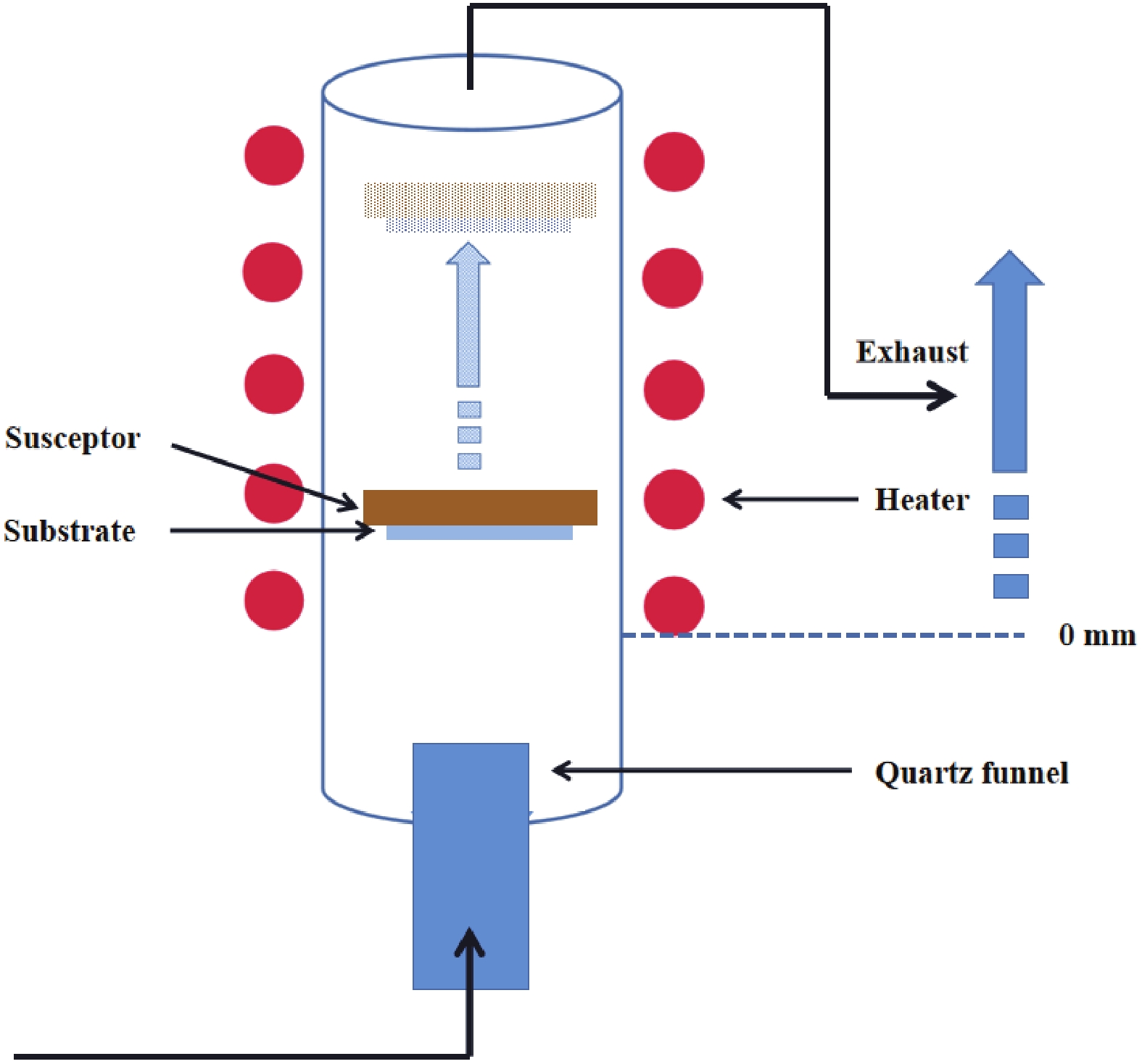
Fig. 1.
(Color online) Schematic of a vertical hot-wall mist-CVD.
ARTICLES
Xiaojie Wang1, Wenxiang Mu1, 2, , Jiahui Xie1, Jinteng Zhang1, Yang Li1, , Zhitai Jia1, 3 and Xutang Tao1, 2
Corresponding author: Wenxiang Mu, mwx@sdu.edu.cn; Yang Li, yangli@sdu.edu.cn
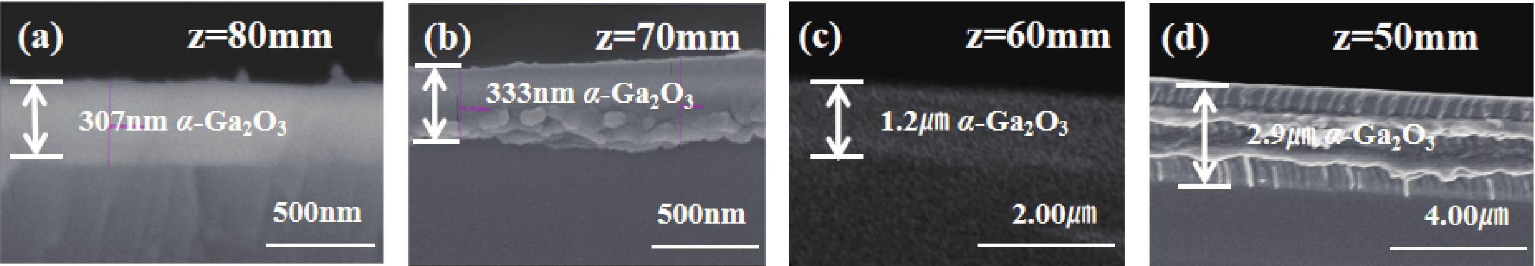
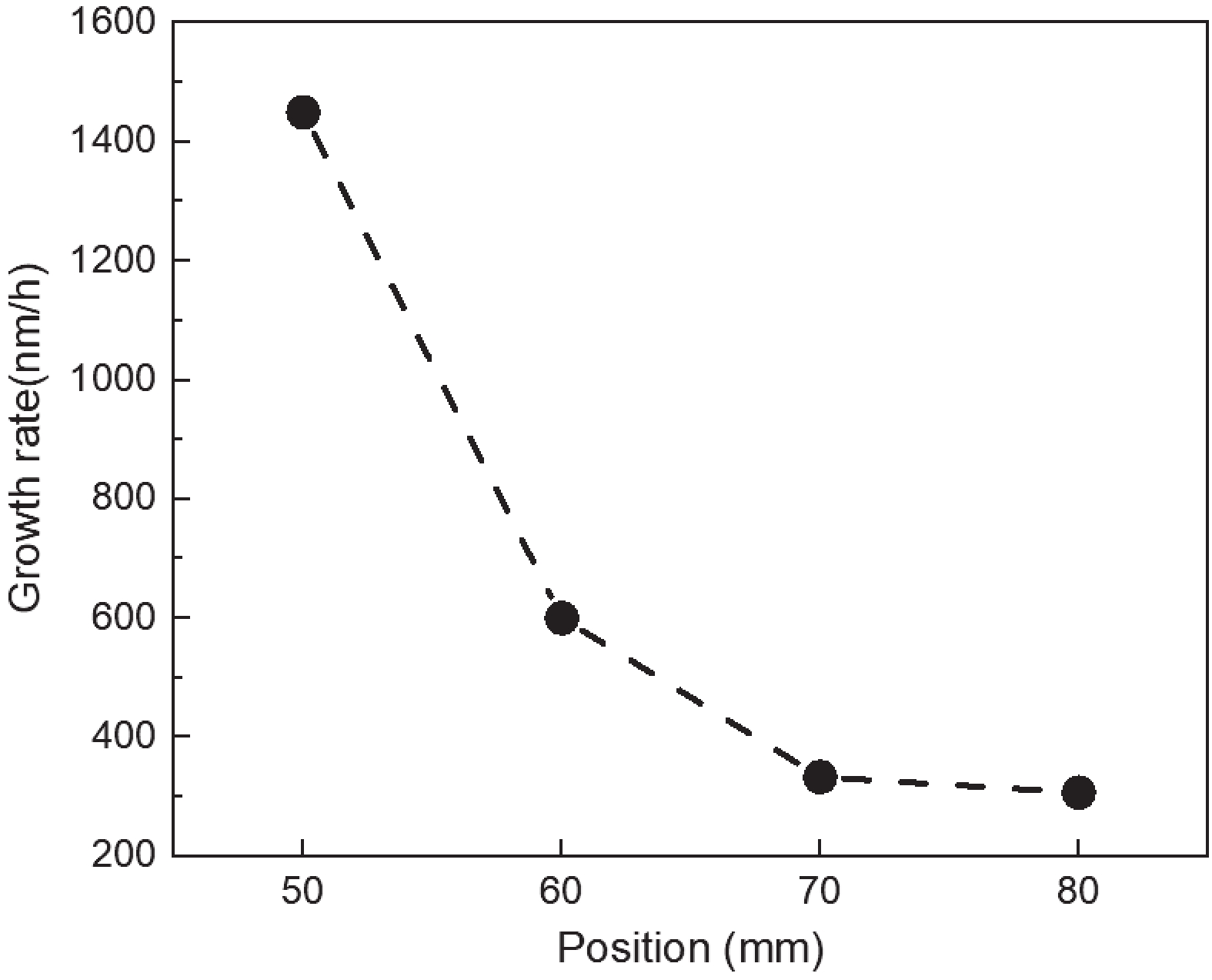
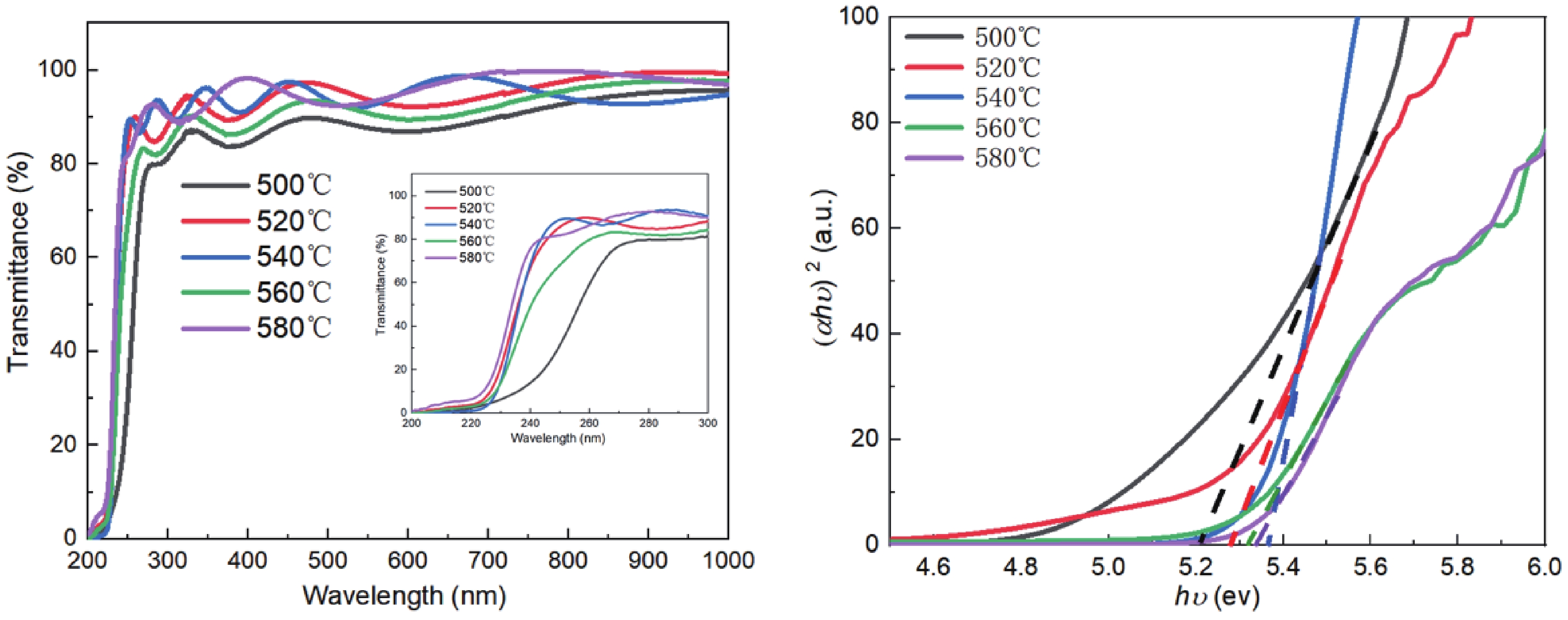
Abstract: High thickness uniformity and large-scale films of α-Ga2O3 are crucial factors for the development of power devices. In this work, a high-quality 2-inch α-Ga2O3 epitaxial film on c-plane sapphire substrates was prepared by the mist-CVD method. The growth rate and phase control mechanisms were systematically investigated. The growth rate of the α-Ga2O3 films was limited by the evaporation of the microdroplets containing gallium acetylacetonate. By adjusting the substrate position (z) from 80 to 50 mm, the growth rate was increased from 307 nm/h to 1.45 μm/h when the growth temperature was fixed at 520 °C. When the growth temperature exceeded 560 °C, ε-Ga2O3 was observed to form at the edges of 2-inch sapphire substrate. Phase control was achieved by adjusting the growth temperature. When the growth temperature was 540 °C and the substrate position was 50 mm, the full-width at half maximum (FWHM) of the rocking curves for the (0006) and (10-14) planes were 0.023° and 1.17°. The screw and edge dislocations were 2.3 × 10⁶ and 3.9 × 1010 cm-2, respectively. Furthermore, the bandgaps and optical transmittance of α-Ga2O3 films grown under different conditions were characterized utilizing UV-visible and near-IR scanning spectra.
Key words: ultra-wide bandgap semiconductor, mist-chemical vapor deposition, epitaxy, alpha-gallium oxide
| [1] |
Roy R, Hill V G, Osborn E F. Polymorphism of Ga2O3 and the system Ga2O3−H2O. J Am Chem Soc, 1952, 74(3), 719 doi: 10.1021/ja01123a039
|
| [2] |
Ricci F, Boschi F, Baraldi A, et al. Theoretical and experimental investigation of optical absorption anisotropy in β-Ga2O3. J Phys Condens Matter, 2016, 28(22), 224005 doi: 10.1088/0953-8984/28/22/224005
|
| [3] |
Kaneko K, Kawanowa H, Ito H, et al. Evaluation of misfit relaxation in α-Ga2O3 epitaxial growth on α-Al2O3 substrate. Jpn J Appl Phys, 2012, 51(2), 020201 doi: 10.1143/JJAP.51.020201
|
| [4] |
Kaneko K, Nomura T, Fujita S, et al. Corundum-structured alpha-phase Ga2O3-Cr2O3-Fe2O3 alloy system for novel functions. Phys Status Solidi C, 2010, 7(10), 2467 doi: 10.1002/pssc.200983896
|
| [5] |
Wang X, Faizan M, Na G, et al. Discovery of new polymorphs of gallium oxides with particle swarm optimization-based structure searches. Adv Electron Mater, 2020, 6(6), 2000119 doi: 10.1002/aelm.202000119
|
| [6] |
Fujita S, Kaneko K. Epitaxial growth of corundum-structured wide band gap III-oxide semiconductor thin films. J Cryst Growth, 2014, 401, 588 doi: 10.1016/j.jcrysgro.2014.02.032
|
| [7] |
Sun H D, Li K H, Castanedo C G T, et al. HCI flow-induced phase change of α-, β-, and ε-Ga2O3 films grown by MOCVD. Cryst Growth Des, 2019, 18(4), 2370 doi: 10.1021/acs.cgd.7b01791
|
| [8] |
Bhuiyan AFMAU, Feng Z X, Huang H L, et al. Metalorganic chemical vapor deposition of α-Ga2O3 and α-(AlxGa1-x)2O3 thin films on m-plane sapphire substrates. APL Mater, 2022, 9(10), 101109 doi: 10.1063/5.0065087
|
| [9] |
Oshima Y, Vilora E G, Shimamura K, et al. Halide vapor phase epitaxy of twin-free α-Ga2O3 on sapphire (0001) substrates. Appl Phys Express, 2015, 8(5), 055501 doi: 10.7567/APEX.8.055501
|
| [10] |
Son H, Jeon D W. Optimization of the growth temperature of α-Ga2O3 epilayers growth by halide vapor phase epitaxy. J Alloys Compd, 2018, 773, 631 doi: 10.1016/j.jallcom.2018.09.230
|
| [11] |
Oshima Y, Kawara K, Oshima T, et al. Rapid growth of α-Ga2O3 by HCl-boosted halide vapor phase epitaxy and effect of precursor supply conditions on crystal properties. Semicond Sci Technol, 2020, 35(5), 055022 doi: 10.1088/1361-6641/ab7843
|
| [12] |
Fujita S, Shinohara D, et al. Heteroepitaxy of corundum-structured α-Ga2O3 thin films on α-Al2O3 substrates by ultrasonic mist chemical vapor deposition. Jpn J Appl Phys, 2008, 47(9), 7311 doi: 10.1143/JJAP.47.7311
|
| [13] |
Hao J G, Ma T C, Chen X H, et al. Phase tailoring and wafer-scale uniform hetero-epitaxy of metastable-phased corundum α-Ga2O3 on sapphire. Appl Surf Sci, 2020, 513, 145871 doi: 10.1016/j.apsusc.2020.145871
|
| [14] |
Park S Y, Ha M T, Kim K H, et al. Enhanced thickness uniformity of large-scale α-Ga2O3 epilayers grown by vertical hot-wall mist chemical vapor deposition. Ceram Int, 2022, 48, 5075 doi: 10.1016/j.ceramint.2021.11.045
|
| [15] |
Ma T C, Chen X H, Ren F F, et al. Heteroepitaxial growth of thick α-Ga2O3 film on sapphire (0001) by MIST-CVD technique. J Semicond, 2019, 40, 012804 doi: 10.1088/1674-4926/40/1/012804
|
| [16] |
El Atab N, Chowdhury F, Ulusoy T G, et al. ~3-nm ZnO nanoislands deposition and application in charge trapping memory grown by single ALD step. Sci Rep, 2017, 6, 38712 doi: 10.1038/srep38712
|
| [17] |
Kim K H, Ha M T, Kwon Y J, et al. Growth of 2-inch α-Ga2O3 epilayers via rear-flow-controlled mist chemical vapor deposition. ECS J Solid State Sci Technol, 2019, 8(7), Q3165 doi: 10.1149/2.0301907jss
|
| [18] |
Akaiwa K, Ichino K. Electrical properties of Sn-doped α-Ga2O3 films on m-plane sapphire substrates grown by mist chemical vapor deposition. Phys Status Solidi A, 2020, 217(3), 1900632 doi: 10.1002/pssa.201900632
|
| [19] |
Xu Y, Zhang C F, Cheng Y L, et al. Influence of carrier gases on the quality of epitaxial corundum-structured α-Ga2O3 films grown by mist chemical vapor deposition method. Mater, 2019, 12(22), 3670 doi: 10.3390/ma12223670
|
| [20] |
Park S Y, Ha M T, Kim K H, et al. Enhanced thickness uniformity of large-scale α-Ga2O3 epilayers grown by vertical hot-wall mist chemical vapor deposition. Ceram Int, 2020, 48(4), 5075 doi: j.ceramint.2021.11.045
|
| [21] |
Ha Mt, Kim K H, Shin Y J, et al. Leidenfrost Motion of water microdroplets on surface substrate: Epitaxy of gallium oxide via mist chemical vapor deposition. Adv Mater, 2021, 8, 2001895 doi: 10.1002/admi.202001895
|
| [22] |
Machon D, Mcmillan P F, Xu B, et al. High-pressure study of the β-to-α transition in Ga2O3. Phys Rev, 2006, 73(9), 094125 doi: 10.1103/PhysRevB.73.094125
|
| [23] |
Akaiwa K, Fujita S, et al. Electrical conductive corundum-structured α-Ga2O3 thin films on sapphire with tin-doping grown by spray-assisted mist chemical vapor deposition. Jpn J Appl Phys, 2012, 51(7), 070203 doi: 10.1143/JJAP.51.070203
|
| [24] |
Oshima Y, Villora E G, Matsushita Y, et al. Epitaxial growth of phase-pure ε-Ga2O3 by halide vapor phase epitaxy. J Appl Phys, 2015, 118(8), 085301 doi: 10.1063/1.4929417
|
| [25] |
Ye J D, Gu S L, Liu W, et al. Competitive adsorption and two-site occupation effects in metal-organic chemical vapor deposition of ZnO. Appl Phys Lett, 2007, 90(17), 174107 doi: 10.1063/1.2731529
|


Article views: 1586 Times PDF downloads: 183 Times Cited by: 0 Times
Received: 30 January 2023 Revised: 27 February 2023 Online: Accepted Manuscript: 03 April 2023Uncorrected proof: 11 April 2023Corrected proof: 25 May 2023Published: 08 June 2023
| Citation: |
Xiaojie Wang, Wenxiang Mu, Jiahui Xie, Jinteng Zhang, Yang Li, Zhitai Jia, Xutang Tao. Rapid epitaxy of 2-inch and high-quality α-Ga2O3 films by mist-CVD method[J]. Journal of Semiconductors, 2023, 44(6): 062803. doi: 10.1088/1674-4926/44/6/062803
****
X J Wang, W X Mu, J H Xie, J T Zhang, Y Li, Z T Jia, X T Tao. Rapid epitaxy of 2-inch and high-quality α-Ga2O3 films by mist-CVD method[J]. J. Semicond, 2023, 44(6): 062803. doi: 10.1088/1674-4926/44/6/062803

|
 Xiaojie Wang:received his BS degree from Wuhan University of Science and Technology in 2019. He is currently a Master’s student at Shandong University. His research focuses on the preparation of α-Ga2O3 films
 Wenxiang Mu:received his PhD degree in 2018 at Shandong University, and has continued his research there. His research interests focus on the research of ultra-wide bandgap semiconductor Ga2O3
 Yang Li:received her PhD degree in 2018 from Shandong University. From 2018 to 2020, she was a postdoc in Shandong University. She is currently an associate professor in Shandong University, Jinan, China. Her current research interests include ultra-wide bandgap semiconductor materials and photoelectric functional crystals
| [1] |
Roy R, Hill V G, Osborn E F. Polymorphism of Ga2O3 and the system Ga2O3−H2O. J Am Chem Soc, 1952, 74(3), 719 doi: 10.1021/ja01123a039
|
| [2] |
Ricci F, Boschi F, Baraldi A, et al. Theoretical and experimental investigation of optical absorption anisotropy in β-Ga2O3. J Phys Condens Matter, 2016, 28(22), 224005 doi: 10.1088/0953-8984/28/22/224005
|
| [3] |
Kaneko K, Kawanowa H, Ito H, et al. Evaluation of misfit relaxation in α-Ga2O3 epitaxial growth on α-Al2O3 substrate. Jpn J Appl Phys, 2012, 51(2), 020201 doi: 10.1143/JJAP.51.020201
|
| [4] |
Kaneko K, Nomura T, Fujita S, et al. Corundum-structured alpha-phase Ga2O3-Cr2O3-Fe2O3 alloy system for novel functions. Phys Status Solidi C, 2010, 7(10), 2467 doi: 10.1002/pssc.200983896
|
| [5] |
Wang X, Faizan M, Na G, et al. Discovery of new polymorphs of gallium oxides with particle swarm optimization-based structure searches. Adv Electron Mater, 2020, 6(6), 2000119 doi: 10.1002/aelm.202000119
|
| [6] |
Fujita S, Kaneko K. Epitaxial growth of corundum-structured wide band gap III-oxide semiconductor thin films. J Cryst Growth, 2014, 401, 588 doi: 10.1016/j.jcrysgro.2014.02.032
|
| [7] |
Sun H D, Li K H, Castanedo C G T, et al. HCI flow-induced phase change of α-, β-, and ε-Ga2O3 films grown by MOCVD. Cryst Growth Des, 2019, 18(4), 2370 doi: 10.1021/acs.cgd.7b01791
|
| [8] |
Bhuiyan AFMAU, Feng Z X, Huang H L, et al. Metalorganic chemical vapor deposition of α-Ga2O3 and α-(AlxGa1-x)2O3 thin films on m-plane sapphire substrates. APL Mater, 2022, 9(10), 101109 doi: 10.1063/5.0065087
|
| [9] |
Oshima Y, Vilora E G, Shimamura K, et al. Halide vapor phase epitaxy of twin-free α-Ga2O3 on sapphire (0001) substrates. Appl Phys Express, 2015, 8(5), 055501 doi: 10.7567/APEX.8.055501
|
| [10] |
Son H, Jeon D W. Optimization of the growth temperature of α-Ga2O3 epilayers growth by halide vapor phase epitaxy. J Alloys Compd, 2018, 773, 631 doi: 10.1016/j.jallcom.2018.09.230
|
| [11] |
Oshima Y, Kawara K, Oshima T, et al. Rapid growth of α-Ga2O3 by HCl-boosted halide vapor phase epitaxy and effect of precursor supply conditions on crystal properties. Semicond Sci Technol, 2020, 35(5), 055022 doi: 10.1088/1361-6641/ab7843
|
| [12] |
Fujita S, Shinohara D, et al. Heteroepitaxy of corundum-structured α-Ga2O3 thin films on α-Al2O3 substrates by ultrasonic mist chemical vapor deposition. Jpn J Appl Phys, 2008, 47(9), 7311 doi: 10.1143/JJAP.47.7311
|
| [13] |
Hao J G, Ma T C, Chen X H, et al. Phase tailoring and wafer-scale uniform hetero-epitaxy of metastable-phased corundum α-Ga2O3 on sapphire. Appl Surf Sci, 2020, 513, 145871 doi: 10.1016/j.apsusc.2020.145871
|
| [14] |
Park S Y, Ha M T, Kim K H, et al. Enhanced thickness uniformity of large-scale α-Ga2O3 epilayers grown by vertical hot-wall mist chemical vapor deposition. Ceram Int, 2022, 48, 5075 doi: 10.1016/j.ceramint.2021.11.045
|
| [15] |
Ma T C, Chen X H, Ren F F, et al. Heteroepitaxial growth of thick α-Ga2O3 film on sapphire (0001) by MIST-CVD technique. J Semicond, 2019, 40, 012804 doi: 10.1088/1674-4926/40/1/012804
|
| [16] |
El Atab N, Chowdhury F, Ulusoy T G, et al. ~3-nm ZnO nanoislands deposition and application in charge trapping memory grown by single ALD step. Sci Rep, 2017, 6, 38712 doi: 10.1038/srep38712
|
| [17] |
Kim K H, Ha M T, Kwon Y J, et al. Growth of 2-inch α-Ga2O3 epilayers via rear-flow-controlled mist chemical vapor deposition. ECS J Solid State Sci Technol, 2019, 8(7), Q3165 doi: 10.1149/2.0301907jss
|
| [18] |
Akaiwa K, Ichino K. Electrical properties of Sn-doped α-Ga2O3 films on m-plane sapphire substrates grown by mist chemical vapor deposition. Phys Status Solidi A, 2020, 217(3), 1900632 doi: 10.1002/pssa.201900632
|
| [19] |
Xu Y, Zhang C F, Cheng Y L, et al. Influence of carrier gases on the quality of epitaxial corundum-structured α-Ga2O3 films grown by mist chemical vapor deposition method. Mater, 2019, 12(22), 3670 doi: 10.3390/ma12223670
|
| [20] |
Park S Y, Ha M T, Kim K H, et al. Enhanced thickness uniformity of large-scale α-Ga2O3 epilayers grown by vertical hot-wall mist chemical vapor deposition. Ceram Int, 2020, 48(4), 5075 doi: j.ceramint.2021.11.045
|
| [21] |
Ha Mt, Kim K H, Shin Y J, et al. Leidenfrost Motion of water microdroplets on surface substrate: Epitaxy of gallium oxide via mist chemical vapor deposition. Adv Mater, 2021, 8, 2001895 doi: 10.1002/admi.202001895
|
| [22] |
Machon D, Mcmillan P F, Xu B, et al. High-pressure study of the β-to-α transition in Ga2O3. Phys Rev, 2006, 73(9), 094125 doi: 10.1103/PhysRevB.73.094125
|
| [23] |
Akaiwa K, Fujita S, et al. Electrical conductive corundum-structured α-Ga2O3 thin films on sapphire with tin-doping grown by spray-assisted mist chemical vapor deposition. Jpn J Appl Phys, 2012, 51(7), 070203 doi: 10.1143/JJAP.51.070203
|
| [24] |
Oshima Y, Villora E G, Matsushita Y, et al. Epitaxial growth of phase-pure ε-Ga2O3 by halide vapor phase epitaxy. J Appl Phys, 2015, 118(8), 085301 doi: 10.1063/1.4929417
|
| [25] |
Ye J D, Gu S L, Liu W, et al. Competitive adsorption and two-site occupation effects in metal-organic chemical vapor deposition of ZnO. Appl Phys Lett, 2007, 90(17), 174107 doi: 10.1063/1.2731529
|

 WeChat ID
Journal of Semiconductors © 2017 All Rights Reserved 京ICP备05085259号-2

 DownLoad:

