ARTICLES

High threshold voltage enhancement-mode GaN p-FET with Si-rich LPCVD SiNx gate insulator for high hole mobility

Liyang Zhu1, Kuangli Chen1, Ying Ma2, Yong Cai2, Chunhua Zhou1, , Zhaoji Li1, Bo Zhang1 and Qi Zhou1, 3,

+ Author Affiliations

 Corresponding author: Chunhua Zhou, czhou@uestc.edu.cn; Qi Zhou, zhouqi@uestc.edu.cn

PDF

Turn off MathJax

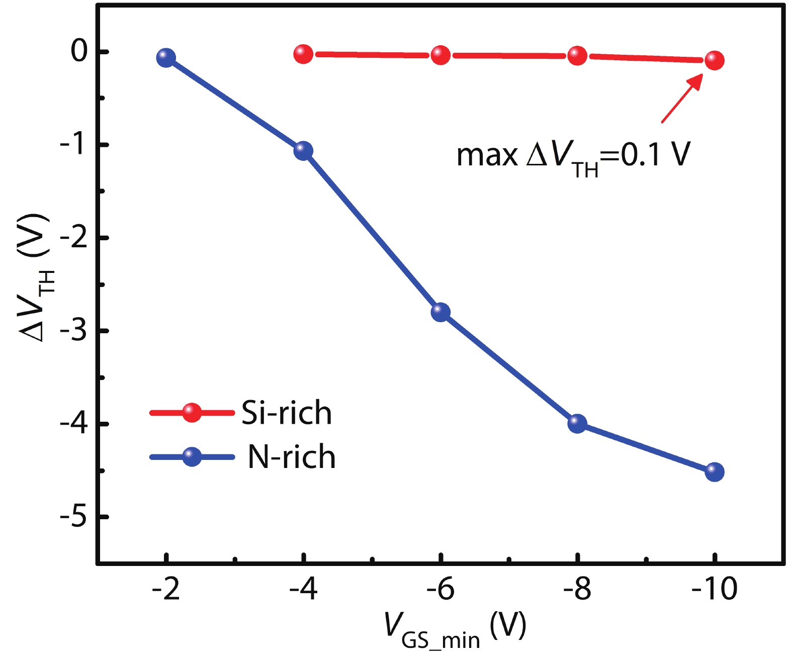
Abstract: In this work, the GaN p-MISFET with LPCVD-SiNx is studied as a gate dielectric to improve device performance. By changing the Si/N stoichiometry of SiNx, it is found that the channel hole mobility can be effectively enhanced with Si-rich SiNx gate dielectric, which leads to a respectably improved drive current of GaN p-FET. The record high channel mobility of 19.4 cm2/(V∙s) was achieved in the device featuring an Enhancement-mode channel. Benefiting from the significantly improved channel mobility, the fabricated E-mode GaN p-MISFET is capable of delivering a decent-high current of 1.6 mA/mm, while simultaneously featuring a negative threshold-voltage (VTH) of –2.3 V (defining at a stringent criteria of 10 μA/mm). The device also exhibits a well pinch-off at 0 V with low leakage current of 1 nA/mm. This suggests that a decent E-mode operation of the fabricated p-FET is obtained. In addition, the VTH shows excellent stability, while the threshold-voltage hysteresis ΔVTH is as small as 0.1 V for a gate voltage swing up to –10 V, which is among the best results reported in the literature. The results indicate that optimizing the Si/N stoichiometry of LPCVD-SiNx is a promising approach to improve the device performance of GaN p-MISFET.

Key words: p-channelGaN p-FETLPCVDchannel mobilityhole mobilityenhancement-mode


[1]
Teo K H, Zhang Y H, Chowdhury N, et al. Emerging GaN technologies for power, RF, digital, and quantum computing applications: Recent advances and prospects. J Appl Phys, 2021, 130, 160902 doi: 10.1063/5.0061555
[2]
Amano H, Baines Y, Beam E, et al. The 2018 GaN power electronics roadmap. J Phys D: Appl Phys, 2018, 51, 163001 doi: 10.1088/1361-6463/aaaf9d
[3]
Trescases O, Murray S K, Jiang W L, et al. GaN power ICs: Reviewing strengths, gaps, and future directions. 2020 IEEE International Electron Devices Meeting (IEDM), 2021, 27.4.1 doi: 10.1109/IEDM13553.2020.9371918
[4]
Dan K. Monolithic GaN power IC technology drives wide bandgap adoption. 2020 IEEE International Electron Devices Meeting (IEDM), 2021, 27.5.1 doi: 10.1109/IEDM13553.2020.9372021
[5]
Hahn H, Reuters B, Kotzea S, et al. First monolithic integration of GaN-based enhancement mode n-channel and p-channel heterostructure field effect transistors. 72nd Device Research Conference, 2014, 259 doi: 10.1109/DRC.2014.6872396
[6]
Nakajima A, Nishizawa S I, Ohashi H, et al. One-chip operation of GaN-based P-channel and N-channel heterojunction field effect transistors. 2014 IEEE 26th International Symposium on Power Semiconductor Devices & IC's (ISPSD), 2014, 241 doi: 10.1109/ISPSD.2014.6856021
[7]
Zheng Z Y, Zhang L, Song W J, et al. Gallium nitride-based complementary logic integrated circuits. Nat Electron, 2021, 4, 595 doi: 10.1038/s41928-021-00611-y
[8]
Niu X R, Hou B, Yang L, et al. Analytical model on the threshold voltage of p-channel heterostructure field-effect transistors on a GaN-based complementary circuit platform. IEEE Trans Electron Devices, 2022, 69, 57 doi: 10.1109/TED.2021.3129712
[9]
Raj A, Krishna A, Hatui N, et al. Demonstration of a GaN/AlGaN superlattice-based p-channel FinFET with high ON-current. IEEE Electron Device Lett, 2020, 41, 220 doi: 10.1109/LED.2019.2963428
[10]
Bader S J, Chaudhuri R, Nomoto K, et al. Gate-recessed E-mode p-channel HFET with high on-current based on GaN/AlN 2D hole gas. IEEE Electron Device Lett, 2018, 39, 1848 doi: 10.1109/LED.2018.2874190
[11]
Raj A, Krishna A, Hatui N, et al. GaN/AlGaN superlattice based E-mode p-channel MES-FinFET with regrown contacts and >50 mA/mm on-current. 2021 IEEE International Electron Devices Meeting (IEDM), 2022, 5.4.1 doi: 10.1109/IEDM19574.2021.9720496
[12]
Chowdhury N, Xie Q Y, Palacios T. Tungsten-gated GaN/AlGaN p-FET with Imax > 120 mA/mm on GaN-on-Si. IEEE Electron Device Lett, 2022, 43, 545 doi: 10.1109/LED.2022.3149659
[13]
Chowdhury N, Xie Q Y, Palacios T. Self-aligned E-mode GaN p-channel FinFET with ION > 100 mA/mm and ION/IOFF > 107. IEEE Electron Device Lett, 2022, 43, 358 doi: 10.1109/LED.2022.3140281
[14]
Du H H, Liu Z H, Hao L, et al. High-performance E-mode p-channel GaN FinFET on silicon substrate with high ION/IOFF and high threshold voltage. IEEE Electron Device Lett, 2022, 43, 705 doi: 10.1109/LED.2022.3155152
[15]
Zheng Z Y, Song W J, Zhang L, et al. High ION and ION/IOFF ratio enhancement−mode buried ratio enhancement−mode buried p-channel GaN MOSFETs on p-GaN gate power HEMT platform. IEEE Electron Device Lett, 2020, 41, 26 doi: 10.1109/LED.2019.2954035
[16]
Yin Y D, Lee K B. High-performance enhancement-mode p-channel GaN MISFETs with steep subthreshold swing. IEEE Electron Device Lett, 2022, 43, 533 doi: 10.1109/LED.2022.3152308
[17]
Chowdhury N, Lemettinen J, Xie Q Y, et al. P-channel GaN transistor based on p-GaN/AlGaN/GaN on Si. IEEE Electron Device Lett, 2019, 40, 1036 doi: 10.1109/LED.2019.2916253
[18]
Chowdhury N, Xie Q Y, Yuan M Y, et al. Regrowth-free GaN-based complementary logic on a Si substrate. IEEE Electron Device Lett, 2020, 41, 820 doi: 10.1109/LED.2020.2987003
[19]
Schroder D K. Semiconductor material and device characterization. Wiley-IEEE Press, 2005
[20]
Makino T. Composition and structure control by source gas ratio in LPCVD SiNx. J Electrochem Soc, 1983, 130, 450 doi: 10.1149/1.2119729
[21]
Zhu L Y, Zhou Q, Chen K L, et al. The modulation effect of LPCVD-Si xNy stoichiometry on 2-DEG characteristic of UTB AlGaN/GaN heterostructure. IEEE Trans Electron Devices, 2022, 69, 4828 doi: 10.1109/TED.2022.3188609
[22]
Jin H, Jiang Q M, Huang S, et al. An enhancement-mode GaN p-FET with improved breakdown voltage. IEEE Electron Device Lett, 2022, 43, 1191 doi: 10.1109/LED.2022.3184998
[23]
Zheng Z Y, Zhang L, Song W J, et al. Threshold voltage instability of enhancement-mode GaN buried p-channel MOSFETs. IEEE Electron Device Lett, 2021, 42, 1584 doi: 10.1109/LED.2021.3114776
[24]
Zhang L, Zheng Z Y, Cheng Y, et al. SiN/in-situ-GaON staggered gate stack on p-GaN for enhanced stability in buried-channel GaN p-FETs. 2021 IEEE International Electron Devices Meeting (IEDM), 2022, 5.3.1 doi: 10.1109/IEDM19574.2021.9720653
[25]
Poncé S, Jena D, Giustino F. Hole mobility of strained GaN from first principles. Phys Rev B, 2019, 100, 085204 doi: 10.1103/PhysRevB.100.085204
[26]
Siddique A, Ahmed R, Anderson J, et al. Effect of reactant gas stoichiometry of in-situ SiNx passivation on structural properties of MOCVD AlGaN/GaN HEMTs. J Cryst Growth, 2019, 517, 28 doi: 10.1016/j.jcrysgro.2019.03.020
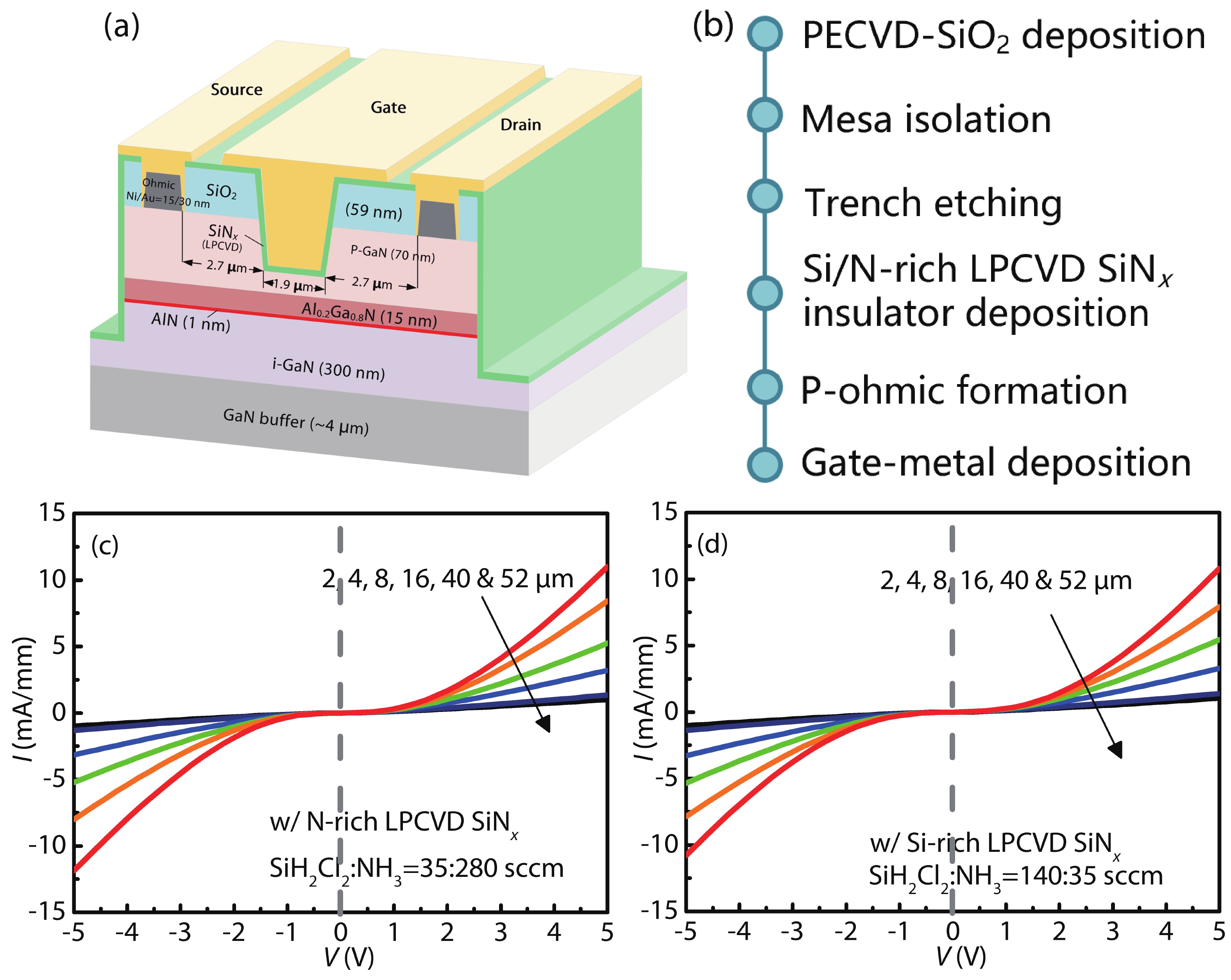
Fig. 1.  (Color online) (a) Epitaxial structure and schematic of the proposed device. (b) The fabrication procedure. The I–V characteristic measured from TLM for the samples with (c) N-rich LPCVD SiNx and (d) Si-rich LPCVD SiNx.

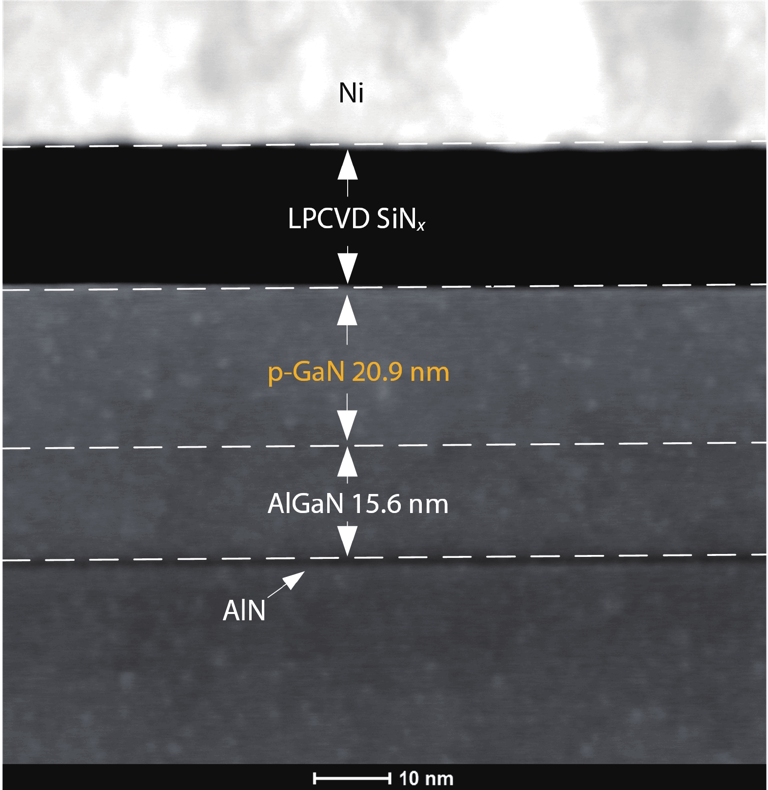
Fig. 2.  (Color online) The focused ion beam section of ~22 nm channel.

Fig. 3.  (Color online) The transfer characteristic of (a) Si-rich sample and (b) N-rich sample. The output characteristic of (c) Si-rich sample and (d) N-rich.

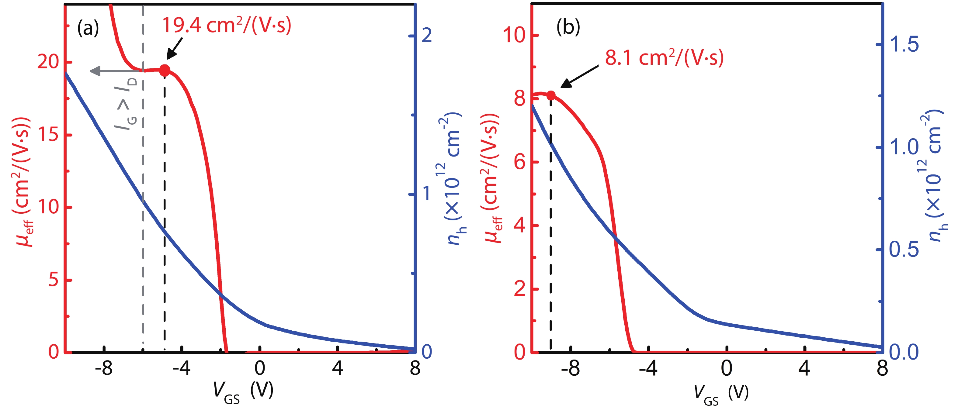
Fig. 4.  (Color online) The μeff and the nh of (a) Si-rich and (b) N-rich sample with ~48 nm trench.

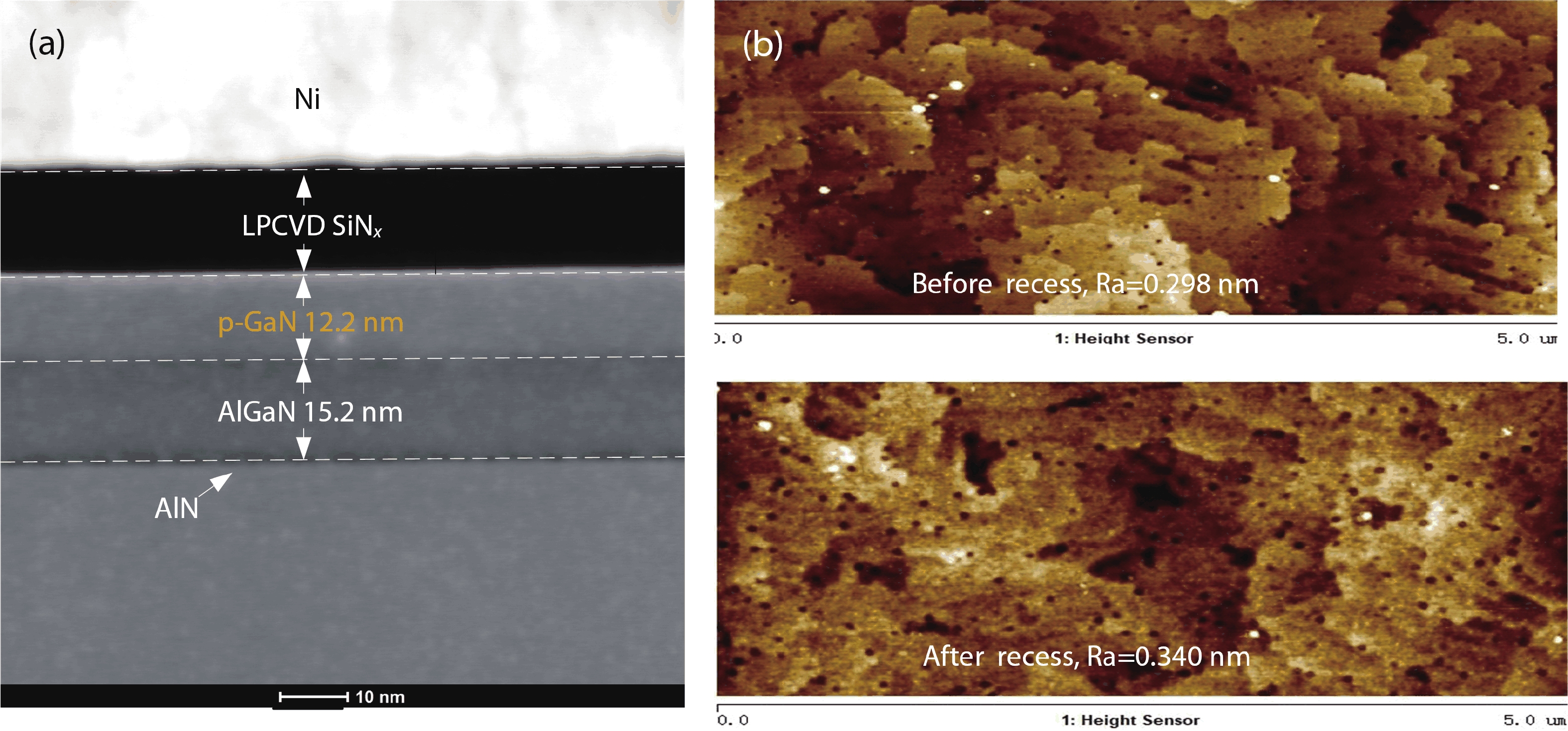
Fig. 5.  (Color online) (a) The focused ion beam section of ~12 nm channel. (b) The surface morphology characterized before/after recess.

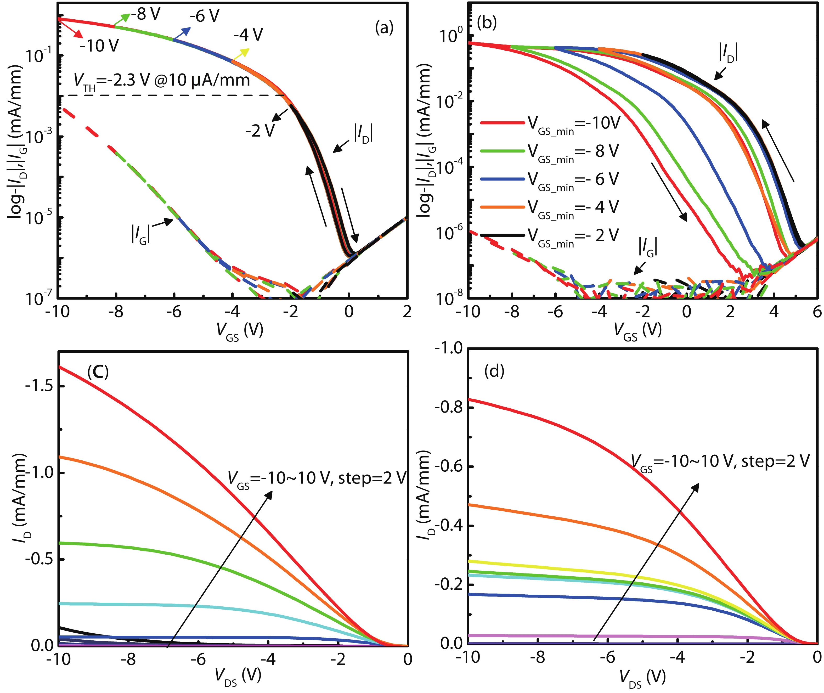
Fig. 6.  (Color online) The transfer characteristic of (a) Si-rich sample and (b) N-rich sample. The output characteristic of (c) Si-rich sample and (d) N-rich.

Fig. 7.  (Color online) The ΔVTH with different VGS sweep ranges.

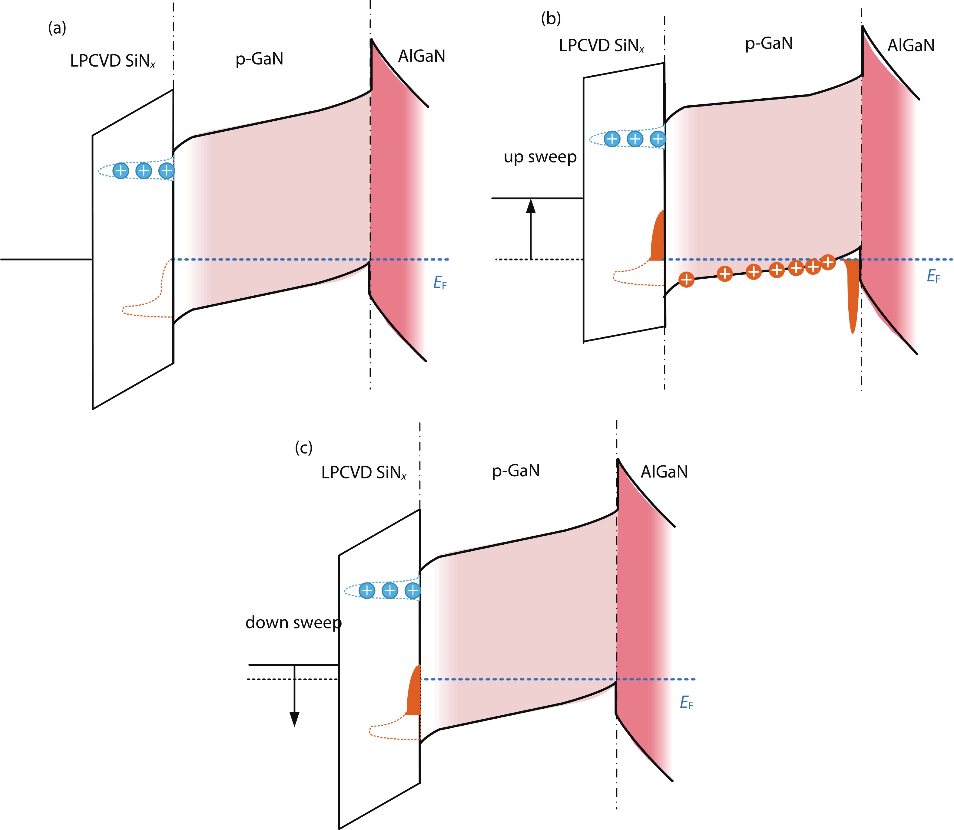
Fig. 8.  (Color online) The Band diagram schematics of the MIS gate of Si-rich sample during the (a) initial state, (b) up sweep and (c) down back.

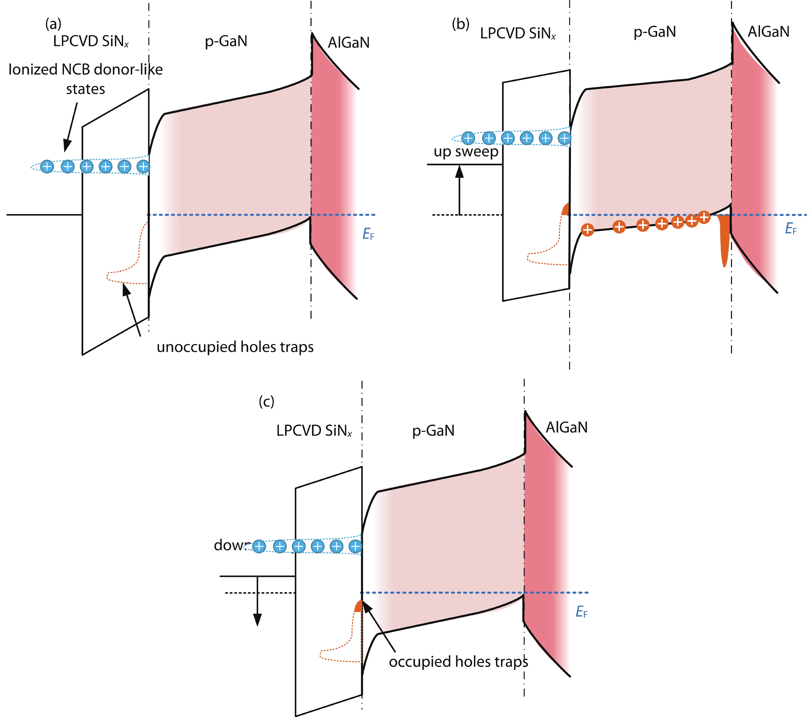
Fig. 9.  (Color online) the Band diagram schematics of the MIS gate of N-rich sample during the (a) initial state, (b) up sweep and (c) down back.

Fig. 10.  (Color online) The μeff and the nh of (a) Si-rich and (b) N-rich sample with ~58 nm trench.

Table 1.   Benchmark of typical parameters of GaN p-FETs.

GroupMobility (cm2/(V∙s))ION/IOFF fVTH (V)ΔVTH (V@VGS_min)RON (kΩ∙mm)
This work19.4a5×105−2.3c−0.1 (@-10 V)5.7
Xidian[14]2b~102−2.2dN. A.0.54
Sheffield[16]11.8a~107−0.73c−0.12 (@−8 V)1
HKUST[24]N. A.e~2×10⁷−1.7c~−0.1 (@−6 V)0.65
SINANO[22]11b~106−2.7c−2.4 (@−12 V)0.061
MIT[12]15b~103.5dN. A.2.3
MIT[13]11b~10−0.3dN. A.2.3
MIT[18]10a~102−1N. A.2.4
MIT[17]7.5a~1062N. A.
HKUST[15]10.2b~2×10⁷−1.7cN. A.
a mobility in channel; b mobility in access region;
c defined at ID = 0.01 mA/mm; d defined by linear-extrapolation;
e N. A. is abbreviation for “not available”; f IOFF in here was the current when VGS is biased to 0 V.
DownLoad: CSV
[1]
Teo K H, Zhang Y H, Chowdhury N, et al. Emerging GaN technologies for power, RF, digital, and quantum computing applications: Recent advances and prospects. J Appl Phys, 2021, 130, 160902 doi: 10.1063/5.0061555
[2]
Amano H, Baines Y, Beam E, et al. The 2018 GaN power electronics roadmap. J Phys D: Appl Phys, 2018, 51, 163001 doi: 10.1088/1361-6463/aaaf9d
[3]
Trescases O, Murray S K, Jiang W L, et al. GaN power ICs: Reviewing strengths, gaps, and future directions. 2020 IEEE International Electron Devices Meeting (IEDM), 2021, 27.4.1 doi: 10.1109/IEDM13553.2020.9371918
[4]
Dan K. Monolithic GaN power IC technology drives wide bandgap adoption. 2020 IEEE International Electron Devices Meeting (IEDM), 2021, 27.5.1 doi: 10.1109/IEDM13553.2020.9372021
[5]
Hahn H, Reuters B, Kotzea S, et al. First monolithic integration of GaN-based enhancement mode n-channel and p-channel heterostructure field effect transistors. 72nd Device Research Conference, 2014, 259 doi: 10.1109/DRC.2014.6872396
[6]
Nakajima A, Nishizawa S I, Ohashi H, et al. One-chip operation of GaN-based P-channel and N-channel heterojunction field effect transistors. 2014 IEEE 26th International Symposium on Power Semiconductor Devices & IC's (ISPSD), 2014, 241 doi: 10.1109/ISPSD.2014.6856021
[7]
Zheng Z Y, Zhang L, Song W J, et al. Gallium nitride-based complementary logic integrated circuits. Nat Electron, 2021, 4, 595 doi: 10.1038/s41928-021-00611-y
[8]
Niu X R, Hou B, Yang L, et al. Analytical model on the threshold voltage of p-channel heterostructure field-effect transistors on a GaN-based complementary circuit platform. IEEE Trans Electron Devices, 2022, 69, 57 doi: 10.1109/TED.2021.3129712
[9]
Raj A, Krishna A, Hatui N, et al. Demonstration of a GaN/AlGaN superlattice-based p-channel FinFET with high ON-current. IEEE Electron Device Lett, 2020, 41, 220 doi: 10.1109/LED.2019.2963428
[10]
Bader S J, Chaudhuri R, Nomoto K, et al. Gate-recessed E-mode p-channel HFET with high on-current based on GaN/AlN 2D hole gas. IEEE Electron Device Lett, 2018, 39, 1848 doi: 10.1109/LED.2018.2874190
[11]
Raj A, Krishna A, Hatui N, et al. GaN/AlGaN superlattice based E-mode p-channel MES-FinFET with regrown contacts and >50 mA/mm on-current. 2021 IEEE International Electron Devices Meeting (IEDM), 2022, 5.4.1 doi: 10.1109/IEDM19574.2021.9720496
[12]
Chowdhury N, Xie Q Y, Palacios T. Tungsten-gated GaN/AlGaN p-FET with Imax > 120 mA/mm on GaN-on-Si. IEEE Electron Device Lett, 2022, 43, 545 doi: 10.1109/LED.2022.3149659
[13]
Chowdhury N, Xie Q Y, Palacios T. Self-aligned E-mode GaN p-channel FinFET with ION > 100 mA/mm and ION/IOFF > 107. IEEE Electron Device Lett, 2022, 43, 358 doi: 10.1109/LED.2022.3140281
[14]
Du H H, Liu Z H, Hao L, et al. High-performance E-mode p-channel GaN FinFET on silicon substrate with high ION/IOFF and high threshold voltage. IEEE Electron Device Lett, 2022, 43, 705 doi: 10.1109/LED.2022.3155152
[15]
Zheng Z Y, Song W J, Zhang L, et al. High ION and ION/IOFF ratio enhancement−mode buried ratio enhancement−mode buried p-channel GaN MOSFETs on p-GaN gate power HEMT platform. IEEE Electron Device Lett, 2020, 41, 26 doi: 10.1109/LED.2019.2954035
[16]
Yin Y D, Lee K B. High-performance enhancement-mode p-channel GaN MISFETs with steep subthreshold swing. IEEE Electron Device Lett, 2022, 43, 533 doi: 10.1109/LED.2022.3152308
[17]
Chowdhury N, Lemettinen J, Xie Q Y, et al. P-channel GaN transistor based on p-GaN/AlGaN/GaN on Si. IEEE Electron Device Lett, 2019, 40, 1036 doi: 10.1109/LED.2019.2916253
[18]
Chowdhury N, Xie Q Y, Yuan M Y, et al. Regrowth-free GaN-based complementary logic on a Si substrate. IEEE Electron Device Lett, 2020, 41, 820 doi: 10.1109/LED.2020.2987003
[19]
Schroder D K. Semiconductor material and device characterization. Wiley-IEEE Press, 2005
[20]
Makino T. Composition and structure control by source gas ratio in LPCVD SiNx. J Electrochem Soc, 1983, 130, 450 doi: 10.1149/1.2119729
[21]
Zhu L Y, Zhou Q, Chen K L, et al. The modulation effect of LPCVD-Si xNy stoichiometry on 2-DEG characteristic of UTB AlGaN/GaN heterostructure. IEEE Trans Electron Devices, 2022, 69, 4828 doi: 10.1109/TED.2022.3188609
[22]
Jin H, Jiang Q M, Huang S, et al. An enhancement-mode GaN p-FET with improved breakdown voltage. IEEE Electron Device Lett, 2022, 43, 1191 doi: 10.1109/LED.2022.3184998
[23]
Zheng Z Y, Zhang L, Song W J, et al. Threshold voltage instability of enhancement-mode GaN buried p-channel MOSFETs. IEEE Electron Device Lett, 2021, 42, 1584 doi: 10.1109/LED.2021.3114776
[24]
Zhang L, Zheng Z Y, Cheng Y, et al. SiN/in-situ-GaON staggered gate stack on p-GaN for enhanced stability in buried-channel GaN p-FETs. 2021 IEEE International Electron Devices Meeting (IEDM), 2022, 5.3.1 doi: 10.1109/IEDM19574.2021.9720653
[25]
Poncé S, Jena D, Giustino F. Hole mobility of strained GaN from first principles. Phys Rev B, 2019, 100, 085204 doi: 10.1103/PhysRevB.100.085204
[26]
Siddique A, Ahmed R, Anderson J, et al. Effect of reactant gas stoichiometry of in-situ SiNx passivation on structural properties of MOCVD AlGaN/GaN HEMTs. J Cryst Growth, 2019, 517, 28 doi: 10.1016/j.jcrysgro.2019.03.020
  • Search

    Advanced Search >>

    GET CITATION

    shu

    Export: BibTex EndNote

    Article Metrics

    Article views: 772 Times PDF downloads: 122 Times Cited by: 0 Times

    History

    Received: 14 January 2023 Revised: 12 February 2023 Online: Accepted Manuscript: 30 March 2023Uncorrected proof: 06 April 2023Corrected proof: 13 July 2023Published: 10 August 2023

    Catalog

      Email This Article

      User name:
      Email:*请输入正确邮箱
      Code:*验证码错误
      Liyang Zhu, Kuangli Chen, Ying Ma, Yong Cai, Chunhua Zhou, Zhaoji Li, Bo Zhang, Qi Zhou. High threshold voltage enhancement-mode GaN p-FET with Si-rich LPCVD SiNx gate insulator for high hole mobility[J]. Journal of Semiconductors, 2023, 44(8): 082801. doi: 10.1088/1674-4926/44/8/082801 L Y Zhu, K L Chen, Y Ma, Y Cai, C H Zhou, Z J Li, B Zhang, Q Zhou. High threshold voltage enhancement-mode GaN p-FET with Si-rich LPCVD SiNx gate insulator for high hole mobility[J]. J. Semicond, 2023, 44(8): 082801. doi: 10.1088/1674-4926/44/8/082801Export: BibTex EndNote
      Citation:
      Liyang Zhu, Kuangli Chen, Ying Ma, Yong Cai, Chunhua Zhou, Zhaoji Li, Bo Zhang, Qi Zhou. High threshold voltage enhancement-mode GaN p-FET with Si-rich LPCVD SiNx gate insulator for high hole mobility[J]. Journal of Semiconductors, 2023, 44(8): 082801. doi: 10.1088/1674-4926/44/8/082801

      L Y Zhu, K L Chen, Y Ma, Y Cai, C H Zhou, Z J Li, B Zhang, Q Zhou. High threshold voltage enhancement-mode GaN p-FET with Si-rich LPCVD SiNx gate insulator for high hole mobility[J]. J. Semicond, 2023, 44(8): 082801. doi: 10.1088/1674-4926/44/8/082801
      Export: BibTex EndNote

      High threshold voltage enhancement-mode GaN p-FET with Si-rich LPCVD SiNx gate insulator for high hole mobility

      doi: 10.1088/1674-4926/44/8/082801
      More Information
      • Author Bio:

        Liyang Zhu received his B.S. degree from the University of Electronic Science and Technology of China, Chengdu, China, in 2016. He is currently a doctoral candidate with the University of Electronic Science and Technology of China, Chengdu, China

        Qi Zhou received his Ph.D. degree in electronic and computer engineering from the Hong Kong University of Science and Technology, Hong Kong, in 2012. He is currently a professor with the University of Electronic Science and Technology of China, Chengdu, China

      • Corresponding author: czhou@uestc.edu.cnzhouqi@uestc.edu.cn
      • Received Date: 2023-01-14
      • Revised Date: 2023-02-12
      • Available Online: 2023-03-30

      Catalog

        /

        DownLoad:  Full-Size Img  PowerPoint
        Return
        Return