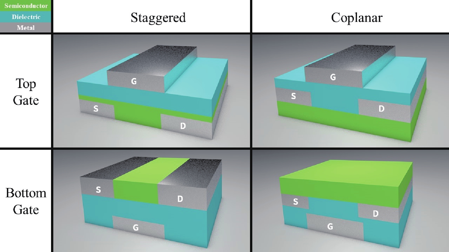
Fig. 1.
(Color online) Schematic diagram of TFT structure classified according to Weimer’s definition and deposition order.
REVIEWS
Feilian Chen1, Meng Zhang1, , Yunhao Wan2, Xindi Xu2, Man Wong3 and Hoi-Sing Kwok3
Corresponding author: Meng Zhang, zhangmeng@connect.ust.hk, ecezhangmeng@gmail.com
Abstract: Indium-tin-zinc oxide (ITZO) thin-film transistor (TFT) technology holds promise for achieving high mobility and offers significant opportunities for commercialization. This paper provides a review of progress made in improving the mobility of ITZO TFTs. This paper begins by describing the development and current status of metal-oxide TFTs, and then goes on to explain the advantages of selecting ITZO as the TFT channel layer. The evaluation criteria for TFTs are subsequently introduced, and the reasons and significance of enhancing mobility are clarified. This paper then explores the development of high-mobility ITZO TFTs from five perspectives: active layer optimization, gate dielectric optimization, electrode optimization, interface optimization, and device structure optimization. Finally, a summary and outlook of the research field are presented.
Key words: thin-film transistor (TFT), indium-tin-zinc oxide (ITZO) TFT, mobility, active matrix (AM) displays
| [1] |
Hirao T, Furuta M, Furuta H, et al. Novel top-gate zinc oxide thin-film transistors (ZnO TFTs) for AMLCDs. Journal of the Society for Information Display, 2007, 15, 17. doi: 10.1889/1.2451545
|
| [2] |
Stewart M, Howell R S, Pires L, et al. Polysilicon TFT technology for active matrix OLED displays. IEEE Trans Electron Devices, 2001, 48, 845 doi: 10.1109/16.918227
|
| [3] |
Sheraw C D, Zhou L, Huang J R, et al. Organic thin-film transistor-driven polymer-dispersed liquid crystal displays on flexible polymeric substrates. Appl Phys Lett, 2002, 80, 1088 doi: 10.1063/1.1448659
|
| [4] |
Kwon J Y, Son K S, Jung J S, et al. Bottom-gate gallium indium zinc oxide thin-film transistor array for high-resolution AMOLED display. IEEE Electron Device Lett, 2008, 29, 1309 doi: 10.1109/LED.2008.2006637
|
| [5] |
Nathan A, Kumar A, Sakariya K, et al. Amorphous silicon thin film transistor circuit integration for organic LED displays on glass and plastic. IEEE J Solid State Circuits, 2004, 39, 1477 doi: 10.1109/JSSC.2004.829373
|
| [6] |
Weimer P K. The TFT A new thin-film transistor. Proc IRE, 1962, 50, 1462 doi: 10.1109/JRPROC.1962.288190
|
| [7] |
Luan S W, Neudeck G W. An experimental study of the source/drain parasitic resistance effects in amorphous silicon thin film transistors. J Appl Phys, 1992, 72, 766 doi: 10.1063/1.351809
|
| [8] |
Sera K, Okumura F, Uchida H, et al. High-performance TFTs fabricated by XeCl excimer laser annealing of hydrogenated amorphous-silicon film. IEEE Trans Electron Devices, 1989, 36, 2868 doi: 10.1109/16.40970
|
| [9] |
Kuriyama H, Kiyama S, Noguchi S, et al. Enlargement of poly-Si film grain size by excimer laser annealing and its application to high-performance poly-Si thin film transistor. Jpn J Appl Phys, 1991, 30, 3700 doi: 10.1143/JJAP.30.3700
|
| [10] |
Brotherton S D. Polycrystalline silicon thin film transistors. Semicond Sci Technol, 1995, 10, 721 doi: 10.1088/0268-1242/10/6/001
|
| [11] |
Meng Z G, Wang M X, Wong M. High performance low temperature metal-induced unilaterally crystallized polycrystalline silicon thin film transistors for system-on-panel applications. IEEE Trans Electron Devices, 2000, 47, 404 doi: 10.1109/16.822287
|
| [12] |
Zhao X F, Wen D Z, Zhuang C C, et al. Fabrication and characteristics of magnetic field sensors based on nano-polysilicon thin-film transistors. J Semicond, 2013, 34, 036001 doi: 10.1088/1674-4926/34/3/036001
|
| [13] |
Cai W S, Li H Y, Li M C, et al. Performance enhancement of solution-processed InZnO thin-film transistors by Al doping and surface passivation. J Semicond, 2022, 43, 034102 doi: 10.1088/1674-4926/43/3/034102
|
| [14] |
Liang Y Y, Kyungsoo J, Velumani S, et al. Effects of interface trap density on the electrical performance of amorphous InSnZnO thin-film transistor. J Semicond, 2015, 36, 024007 doi: 10.1088/1674-4926/36/2/024007
|
| [15] |
Zhu X M, Wu H Z, Wang S J, et al. Optical and electrical properties of N-doped ZnO and fabrication of thin-film transistors. J Semicond, 2009, 30, 033001 doi: 10.1088/1674-4926/30/3/033001
|
| [16] |
Zhu Y, He Y L, Jiang S S, et al. Indium–gallium–zinc–oxide thin-film transistors: Materials, devices, and applications. J Semicond, 2021, 42, 031101 doi: 10.1088/1674-4926/42/3/031101
|
| [17] |
Mittal P, Negi Y S, Singh R K. Impact of source and drain contact thickness on the performance of organic thin film transistors. J Semicond, 2014, 35, 124002 doi: 10.1088/1674-4926/35/12/124002
|
| [18] |
Li Z F, Luo X Y. ADO-phosphonic acid self-assembled monolayer modified dielectrics for organic thin film transistors. J Semicond, 2014, 35, 104004 doi: 10.1088/1674-4926/35/10/104004
|
| [19] |
Lin C L, Cheng M H, Tu C D, et al. Highly reliable integrated gate driver circuit for large TFT-LCD applications. IEEE Electron Device Lett, 2012, 33, 679 doi: 10.1109/LED.2012.2188269
|
| [20] |
Liao C W, He C D, Chen T, et al. Design of integrated amorphous-silicon thin-film transistor gate driver. J Disp Technol, 2013, 9, 7 doi: 10.1109/JDT.2012.2221154
|
| [21] |
Lin C L, Tu C D, Chuang M C, et al. Design of bidirectional and highly stable integrated hydrogenated amorphous silicon gate driver circuits. J Disp Technol, 2011, 7, 10 doi: 10.1109/JDT.2010.2085077
|
| [22] |
Tanaka T, Asuma H, Ogawa K, et al. An LCD addressed by a-Si: H TFTs with peripheral poly-Si TFT circuits. Proceedings of IEEE International Electron Devices Meeting. Washington, DC, USA. IEEE, 2002, 389 doi: 10.1109/IEDM.1993.347327
|
| [23] |
Nomura K, Ohta H, Takagi A, et al. Room-temperature fabrication of transparent flexible thin-film transistors using amorphous oxide semiconductors. Nature, 2004, 432, 488 doi: 10.1038/nature03090
|
| [24] |
Son K S, Kim T S, Jung J S, et al. 4 inch QVGA AMOLED driven by the threshold voltage controlled amorphous GIZO (Ga2O3-In2O3-ZnO) TFT. SID Symp Dig Tech Pap, 2008, 39, 633 doi: 10.1889/1.3069743
|
| [25] |
Lee J H, Kim D H, Yang D J, et al. World’s largest (15-inch) XGA AMLCD panel using IGZO oxide TFT. SID Symp Dig Tech Pap, 2008, 39, 625 doi: 10.1889/1.3069740
|
| [26] |
Park J S, Kim T W, Stryakhilev D, et al. Flexible full color organic light-emitting diode display on polyimide plastic substrate driven by amorphous indium gallium zinc oxide thin-film transistors. Appl Phys Lett, 2009, 95, 013503 doi: 10.1063/1.3159832
|
| [27] |
Park J S, Lim J H. 4-3: Invited paper: High mobility oxide thin-film transistors for AMOLED displays. SID Symp Dig Tech Pap, 2022, 53, 20 doi: https://doi.org/10.1002/sdtp.15405
|
| [28] |
Arai T. Oxide-TFT technologies for next-generation AMOLED displays. J Soc Inf Disp, 2012, 20, 156 doi: 10.1889/JSID20.3.156
|
| [29] |
Lin C L, Lai P C, Lai P C, et al. Pixel circuit with parallel driving scheme for compensating luminance variation based on a-IGZO TFT for AMOLED displays. J Disp Technol, 2016, 12, 1681 doi: 10.1109/JDT.2016.2616507
|
| [30] |
Chen Y F, Lee S H, Kim H, et al. In-pixel temperature sensor for high-luminance active matrix micro-light-emitting diode display using low-temperature polycrystalline silicon and oxide thin-film-transistors. J Soc Inf Disp, 2020, 28, 528 doi: 10.1002/jsid.915
|
| [31] |
Cho D, Moon J, Kihm T Y, et al. 48-4: LTPO technology development for enhanced display performance: Image sticking phenomena, circuit operation and backplane process integration. SID Symp Dig Tech Pap, 2022, 53, 620 doi: 10.1002/sdtp.15564
|
| [32] |
Shiah Y S, Sim K, Shi Y H, et al. Mobility–stability trade-off in oxide thin-film transistors. Nat Electron, 2021, 4, 800 doi: 10.1038/s41928-021-00671-0
|
| [33] |
Shi J L, Zhang J Y, Yang L, et al. Wide bandgap oxide semiconductors: From materials physics to optoelectronic devices. Adv Mater, 2021, 33, 2006230 doi: 10.1002/adma.202006230
|
| [34] |
Noh J Y, Kim H, Nahm H H, et al. Cation composition effects on electronic structures of In-Sn-Zn-O amorphous semiconductors. J Appl Phys, 2013, 113, 183706 doi: 10.1063/1.4803706
|
| [35] |
Fortunato E, Barquinha P, Martins R. Oxide semiconductor thin-film transistors: A review of recent advances. Adv Mater, 2012, 24, 2945 doi: 10.1002/adma.201103228
|
| [36] |
Wallmark J, Johnson H. Field-effect transistors: Physics, technology and applications. Prentice-Hall, 1966
|
| [37] |
Petti L, Münzenrieder N, Vogt C, et al. Metal oxide semiconductor thin-film transistors for flexible electronics. Appl Phys Rev, 2016, 3, 021303 doi: 10.1063/1.4953034
|
| [38] |
Jang K, Raja J, Lee Y J, et al. Effects of carrier concentration, indium content, and crystallinity on the electrical properties of indium-tin-zinc-oxide thin-film transistors. IEEE Electron Device Lett, 2013, 34, 1151 doi: 10.1109/LED.2013.2272084
|
| [39] |
Kim S H, Ahn C H, Yun M G, et al. Anomalous tin chemical bonding in indium-zinc-tin oxide films and their thin film transistor performance. J Phys D: Appl Phys, 2014, 47, 485101 doi: 10.1088/0022-3727/47/48/485101
|
| [40] |
Park J, Rim Y S, Li C, et al. Defect-induced instability mechanisms of sputtered amorphous indium tin zinc oxide thin-film transistors. J Appl Phys, 2018, 123, 161568 doi: 10.1063/1.5004148
|
| [41] |
Wu Z D, Zhang H B, Wang X L, et al. Effects of target quality on electrical performance and stability of In-Sn-Zn-O thin-film transistors. IEEE Electron Device Lett, 2021, 42, 529 doi: 10.1109/LED.2021.3062369
|
| [42] |
Jia J J, Torigoshi Y, Kawashima E, et al. Amorphous indium-tin-zinc oxide films deposited by magnetron sputtering with various reactive gases: Spatial distribution of thin film transistor performance. Appl Phys Lett, 2015, 106, 023502 doi: 10.1063/1.4905654
|
| [43] |
Pan T M, Peng B J, Her J L, et al. Effect of in and Zn content on structural and electrical properties of InZnSnO thin-film transistors using an Yb2TiO5 gate dielectric. IEEE Trans Electron Devices, 2017, 64, 2233 doi: 10.1109/TED.2017.2680410
|
| [44] |
Lee D H, Han S Y, Herman G S, et al. Inkjet printed high-mobility indium zinc tin oxide thin film transistors. J Mater Chem, 2009, 19, 3135 doi: 10.1039/b822893k
|
| [45] |
Kim B J, Kim H J, Yoon T S, et al. Solution processed IZTO thin film transistor on silicon nitride dielectric layer. J Ind Eng Chem, 2011, 17, 96 doi: 10.1016/j.jiec.2010.12.003
|
| [46] |
Bukke R N, Mude N N, Saha J K, et al. High performance of a-IZTO TFT by purification of the semiconductor oxide precursor. Adv Mater Interfaces, 2019, 6, 1900277 doi: 10.1002/admi.201900277
|
| [47] |
Sheng J Z, Hong T, Kang D, et al. Design of InZnSnO semiconductor alloys synthesized by supercycle atomic layer deposition and their rollable applications. ACS Appl Mater Interfaces, 2019, 11, 12683 doi: 10.1021/acsami.9b02999
|
| [48] |
Baek I H, Pyeon J J, Han S H, et al. High-performance thin-film transistors of quaternary indium–zinc–tin oxide films grown by atomic layer deposition. ACS Appl Mater Interfaces, 2019, 11, 14892 doi: 10.1021/acsami.9b03331
|
| [49] |
Liu H Y, Hsu W C, Chen J H, et al. Amorphous ITZO thin-film transistors by using ultrasonic spray pyrolysis deposition. IEEE Trans Electron Devices, 2020, 67, 1009 doi: 10.1109/TED.2020.2965949
|
| [50] |
Li R, Dai S Q, Ma Y B, et al. High-performance transparent Li-doped indium-tin-zinc-oxide thin film transistor fabricated by radio frequency magnetron sputtering method. Mater Lett, 2018, 230, 132 doi: 10.1016/j.matlet.2018.07.098
|
| [51] |
Li R, Dai S Q, Su J B, et al. Effect of thermal annealing on the electrical characteristics of an amorphous ITZO: Li thin film transistor fabricated using the magnetron sputtering method. Mater Sci Semicond Process, 2019, 96, 8 doi: 10.1016/j.mssp.2019.02.005
|
| [52] |
Zhang Y P, Zhang H, Yang J, et al. Solution-processed yttrium-doped IZTO semiconductors for high-stability thin film transistor applications. IEEE Trans Electron Devices, 2019, 66, 5170 doi: 10.1109/TED.2019.2949702
|
| [53] |
Zhang H B, Liang L Y, Wang X L, et al. Praseodymium-doped In-Sn-Zn-O TFTs with effective improvement of negative-bias illumination stress stability. IEEE Trans Electron Devices, 2022, 69, 152 doi: 10.1109/TED.2021.3126278
|
| [54] |
Jia J J, Torigoshi Y, Suko A, et al. Effect of nitrogen addition on the structural, electrical, and optical properties of In-Sn-Zn oxide thin films. Appl Surf Sci, 2017, 396, 897 doi: 10.1016/j.apsusc.2016.11.058
|
| [55] |
Li Z Y, Yang H Z, Chen S C, et al. Impact of active layer thickness of nitrogen-doped In–Sn–Zn–O films on materials and thin film transistor performances. J Phys D: Appl Phys, 2018, 51, 175101 doi: 10.1088/1361-6463/aab7db
|
| [56] |
Fuh C S, Liu P T, Huang W H, et al. Effect of annealing on defect elimination for high mobility amorphous indium-zinc-tin-oxide thin-film transistor. IEEE Electron Device Lett, 2014, 35, 1103 doi: 10.1109/LED.2014.2354598
|
| [57] |
Zhong W, Li G Y, Lan L F, et al. Effects of annealing temperature on properties of InSnZnO thin film transistors prepared by Co-sputtering. RSC Adv, 2018, 8, 34817 doi: 10.1039/C8RA06692B
|
| [58] |
Maeng S, Kim H, Choi G, et al. Investigation of electrical performance and operation stability of RF-sputtered InSnZnO thin film transistors by oxygen-ambient rapid thermal annealing. Semicond Sci Technol, 2020, 35, 125019 doi: 10.1088/1361-6641/abbc8f
|
| [59] |
Park S, Park K, Kim H, et al. Light-induced bias stability of crystalline indium-tin-zinc-oxide thin film transistors. Appl Surf Sci, 2020, 526, 146655 doi: 10.1016/j.apsusc.2020.146655
|
| [60] |
Wang X L, Liang L Y, Zhang H B, et al. Huge mobility enhancement of InSnZnO thin-film transistors via Al-induced microstructure regularization. Appl Phys Lett, 2021, 119, 212102 doi: 10.1063/5.0072077
|
| [61] |
Kim G B, On N, Kim T, et al. High mobility IZTO thin-film transistors based on spinel phase formation at low temperature through a catalytic chemical reaction. Small Methods, 2023, 2201522 doi: 10.1002/smtd.202201522
|
| [62] |
Tseng W H, Fang S W, Lu C Y, et al. The effect of nitrous oxide plasma treatment on the bias temperature stress of metal oxide thin film transistors with high mobility. Solid State Electron, 2015, 103, 173 doi: 10.1016/j.sse.2014.07.017
|
| [63] |
Wang B H, Huang W, Chi L F, et al. High- k gate dielectrics for emerging flexible and stretchable electronics. Chem Rev, 2018, 118, 5690 doi: 10.1021/acs.chemrev.8b00045
|
| [64] |
Bak Y G, Park J W, Park Y J, et al. In-Zn-Sn-O thin film based transistor with high-k HfO2 dielectric. Thin Solid Films, 2022, 753, 139290 doi: 10.1016/j.tsf.2022.139290
|
| [65] |
Jang K, Raja J, Kim J, et al. Bias-stability improvement using Al2O3 interfacial dielectrics in a-InSnZnO thin-film transistors. Semicond Sci Technol, 2013, 28, 085015 doi: 10.1088/0268-1242/28/8/085015
|
| [66] |
Raja J, Nguyen C P T, Lee C M, et al. Improved data retention of InSnZnO nonvolatile memory by H2O2 treated Al2O3 tunneling layer: A cost-effective method. IEEE Electron Device Lett, 2016, 37, 1272 doi: 10.1109/LED.2016.2599559
|
| [67] |
Javey A, Kim H, Brink M, et al. High-κ dielectrics for advanced carbon-nanotube transistors and logic gates. Nat Mater, 2002, 1, 241 doi: 10.1038/nmat769
|
| [68] |
Ruan D B, Liu P T, Chiu Y C, et al. Investigation of low operation voltage InZnSnO thin-film transistors with different high-k gate dielectric by physical vapor deposition. Thin Solid Films, 2018, 660, 885 doi: 10.1016/j.tsf.2018.02.036
|
| [69] |
Bukke R N, Avis C, Naik M N, et al. Remarkable increase in field effect mobility of amorphous IZTO thin-film transistors with purified ZrOx gate insulator. IEEE Electron Device Lett, 2018, 39, 371 doi: 10.1109/LED.2018.2791633
|
| [70] |
Bukke R N, Naik Mude N, Lee J, et al. Effect of Hf alloy in ZrOx gate insulator for solution processed a-IZTO thin film transistors. IEEE Electron Device Lett, 2019, 40, 32 doi: 10.1109/LED.2018.2880177
|
| [71] |
Kim M, Jeong H J, Sheng J Z, et al. The impact of plasma-enhanced atomic layer deposited ZrSiOx insulators on low voltage operated In-Sn-Zn-O thin film transistors. Ceram Int, 2019, 45, 19166 doi: 10.1016/j.ceramint.2019.06.163
|
| [72] |
Choi W H, Jeon W, Park J S. Nanoscale surface engineering of a high- k ZrO2/SiO2 gate insulator for a high performance ITZO TFT via plasma-enhanced atomic layer deposition. J Mater Chem C, 2020, 8, 13342 doi: 10.1039/D0TC02419H
|
| [73] |
Zhong W, Zhang J F, Liu Y, et al. Gate dielectric treated by self-assembled monolayers (SAMs) to enhance the performance of InSnZnO thin-film transistors. IEEE Trans Electron Devices, 2022, 69, 2398 doi: 10.1109/TED.2022.3155709
|
| [74] |
Nguyen C P T, Trinh T T, Raja J, et al. Source/drain metallization effects on the specific contact resistance of indium tin zinc oxide thin film transistors. Mater Sci Semicond Process, 2015, 39, 649 doi: 10.1016/j.mssp.2015.05.069
|
| [75] |
Park J, Shin M, Yi J. Comparative study of aluminum and nickel contact electrodes for indium–tin–zinc oxide thin film transistors using oxygen vacancy diffusion model. Mater Sci Semicond Process, 2020, 120, 105253 doi: 10.1016/j.mssp.2020.105253
|
| [76] |
Cho S H, Lee Y U, Lee J S, et al. Effect of self-assembled monolayer (SAM) on the oxide semiconductor thin film transistor. J Disp Technol, 2012, 8, 35 doi: 10.1109/JDT.2011.2169936
|
| [77] |
Zhong W, Li G Y, Lan L F, et al. InSnZnO thin-film transistors with vapor- phase self-assembled monolayer as passivation layer. IEEE Electron Device Lett, 2018, 39, 1680 doi: 10.1109/LED.2018.2872352
|
| [78] |
Zhong W, Yao R H, Liu Y, et al. Effect of self-assembled monolayers (SAMs) as surface passivation on the flexible a-InSnZnO thin-film transistors. IEEE Trans Electron Devices, 2020, 67, 3157 doi: 10.1109/TED.2020.3004420
|
| [79] |
Chen Y Y, Li B, Zhong W, et al. InSnZnO thin-film transistors with nitrogenous self-assembled multilayers passivation. IEEE Trans Electron Devices, 2021, 68, 5612 doi: 10.1109/TED.2021.3114267
|
| [80] |
Bukke R N, Avis C, Jang J. Solution-processed amorphous In–Zn–Sn oxide thin-film transistor performance improvement by solution-processed Y2O3 passivation. IEEE Electron Device Lett, 2016, 37, 433 doi: 10.1109/LED.2016.2528288
|
| [81] |
Zhong W, Kang L Y, Deng S B, et al. Effect of Sc2O3 passivation layer on the electrical characteristics and stability of InSnZnO thin-film transistors. IEEE Trans Electron Devices, 2021, 68, 4956 doi: 10.1109/TED.2021.3105486
|
| [82] |
Shi Y H, Shiah Y S, Sim K, et al. High-performance a-ITZO TFTs with high bias stability enabled by self-aligned passivation using a-GaOx. Appl Phys Lett, 2022, 121, 212101 doi: 10.1063/5.0123253
|
| [83] |
Shiah Y S, Sim K, Ueda S, et al. Unintended carbon-related impurity and negative bias instability in high-mobility oxide TFTs. IEEE Electron Device Lett, 2021, 42, 1319 doi: 10.1109/LED.2021.3101654
|
| [84] |
Jeon G J, Yang J, Lee S H, et al. Abnormal thermal instability of Al-InSnZnO thin-film transistor by hydroxyl-induced oxygen vacancy at SiOx/active interface. IEEE Electron Device Lett, 2021, 42, 363 doi: 10.1109/LED.2021.3054859
|
| [85] |
Xia Z H, Lu L, Li J P, et al. Characteristics of elevated-metal metal-oxide thin-film transistors based on indium-tin-zinc oxide. IEEE Electron Device Lett, 2017, 38, 894 doi: 10.1109/LED.2017.2707090
|
| [86] |
Kim J, Kim D H, Cho S I, et al. Channel-shortening effect suppression of a high-mobility self-aligned oxide TFT using trench structure. IEEE Electron Device Lett, 2021, 42, 1798 doi: 10.1109/LED.2021.3125146
|
| [87] |
Lee J, Jin J D, Maeng S, et al. Enhancement of the electrical performance and bias stability of RF-sputtered indium tin zinc oxide thin-film transistors with vertical stoichiometric oxygen control. ACS Appl Electron Mater, 2022, 4, 1800 doi: 10.1021/acsaelm.2c00054
|
| [88] |
Jin J D, Lin X Y, Zhang J W, et al. Low-voltage, high-performance, indium-tin-zinc-oxide thin-film transistors based on dual-channel and anodic-oxide. Adv Electron Mater, 2023, 9, 2201117 doi: 10.1002/aelm.202201117
|
| [89] |
Nguyen C P T, Raja J, Kim S, et al. Enhanced electrical properties of oxide semiconductor thin-film transistors with high conductivity thin layer insertion for the channel region. Appl Surf Sci, 2017, 396, 1472 doi: 10.1016/j.apsusc.2016.11.194
|
| [90] |
Lee M, Jo J W, Kim Y J, et al. Corrugated heterojunction metal-oxide thin-film transistors with high electron mobility via vertical interface manipulation. Adv Mater, 2018, 30, 1804120 doi: 10.1002/adma.201804120
|
| [91] |
Yu W, Zhao D Y, Cai J, et al. Performance enhancement of TiZO thin film transistors by introducing a thin ITO interlayer. IEEE J Electron Devices Soc, 2019, 7, 1302 doi: 10.1109/JEDS.2019.2951738
|
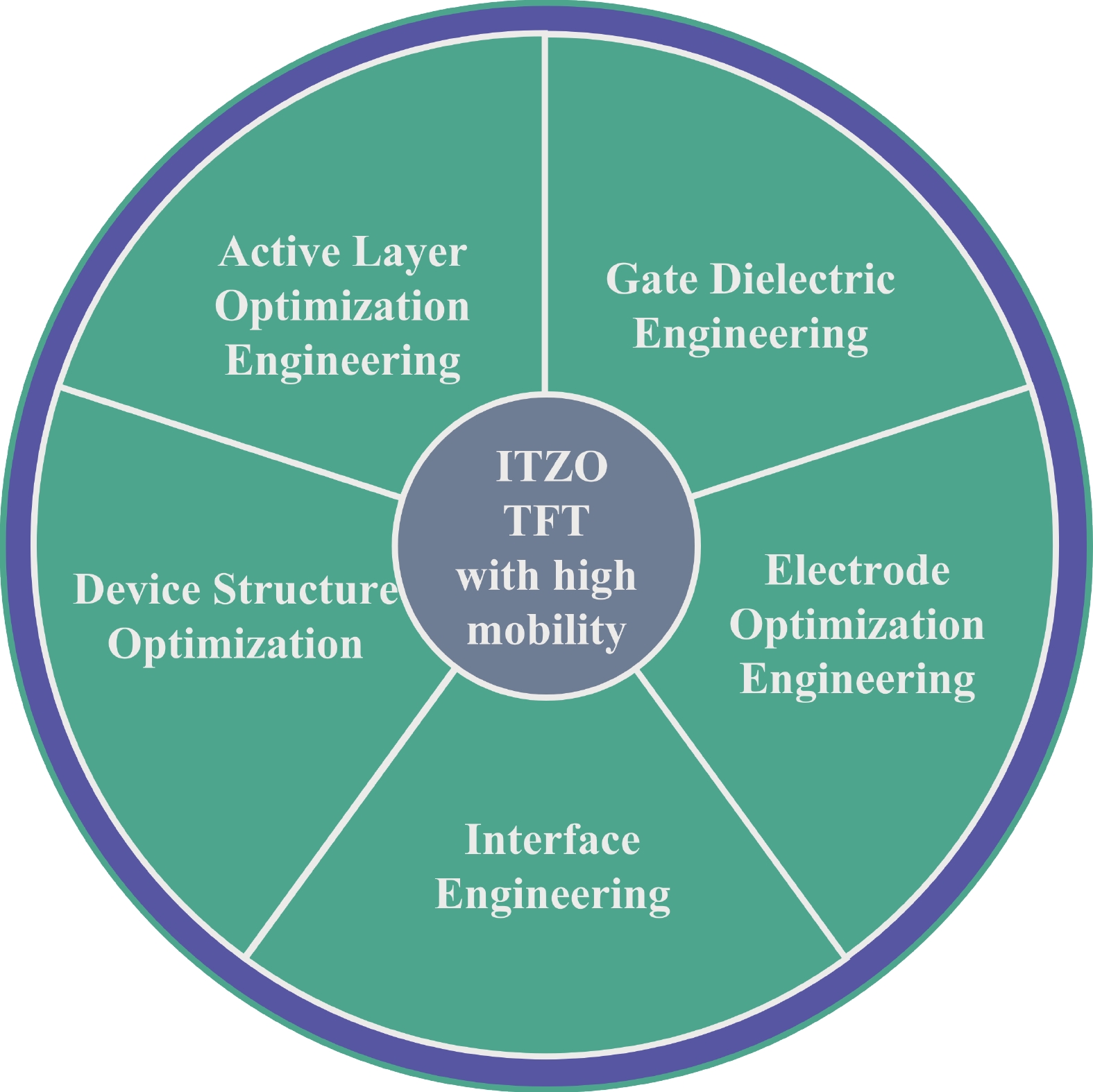

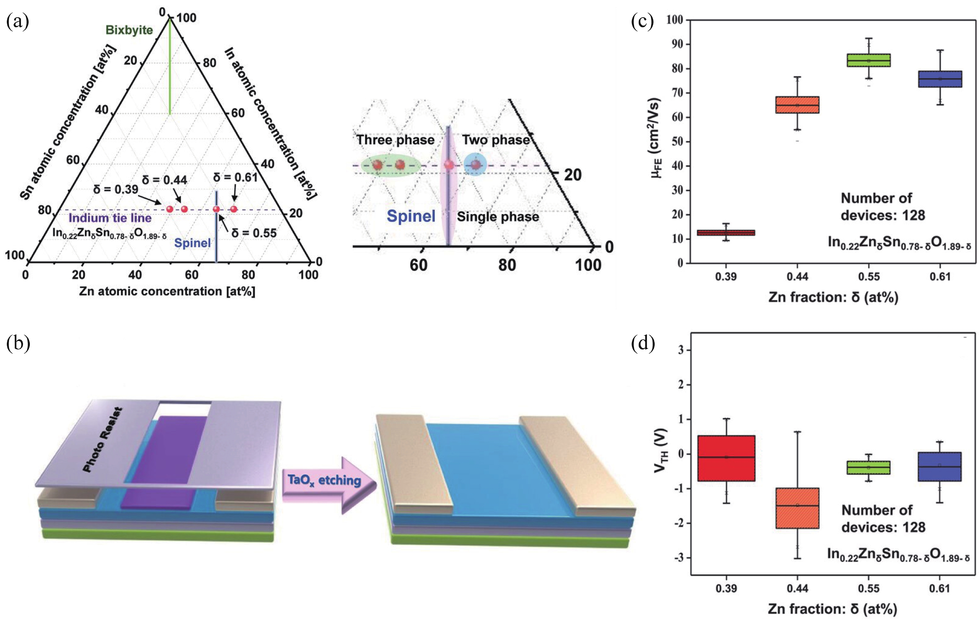
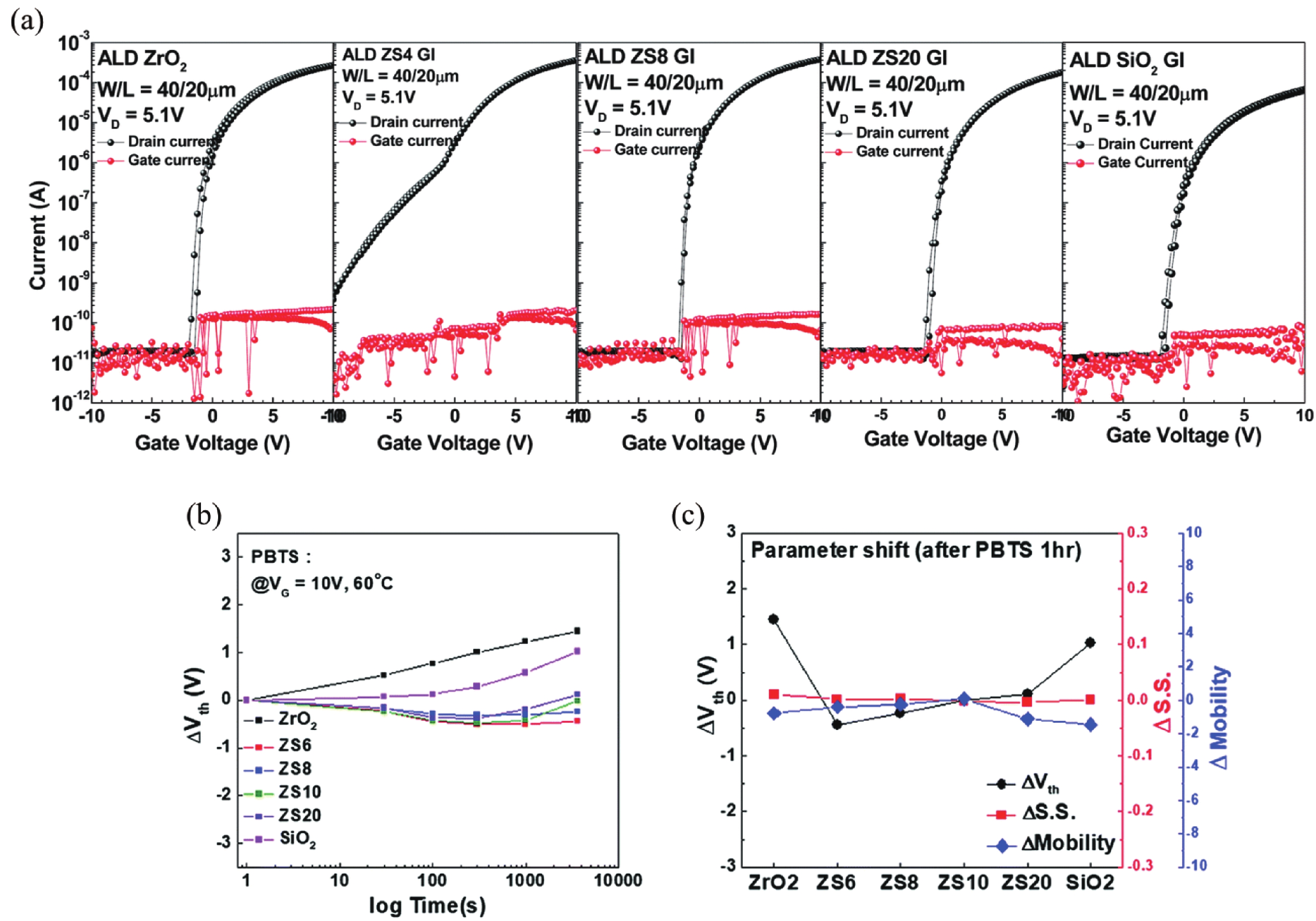

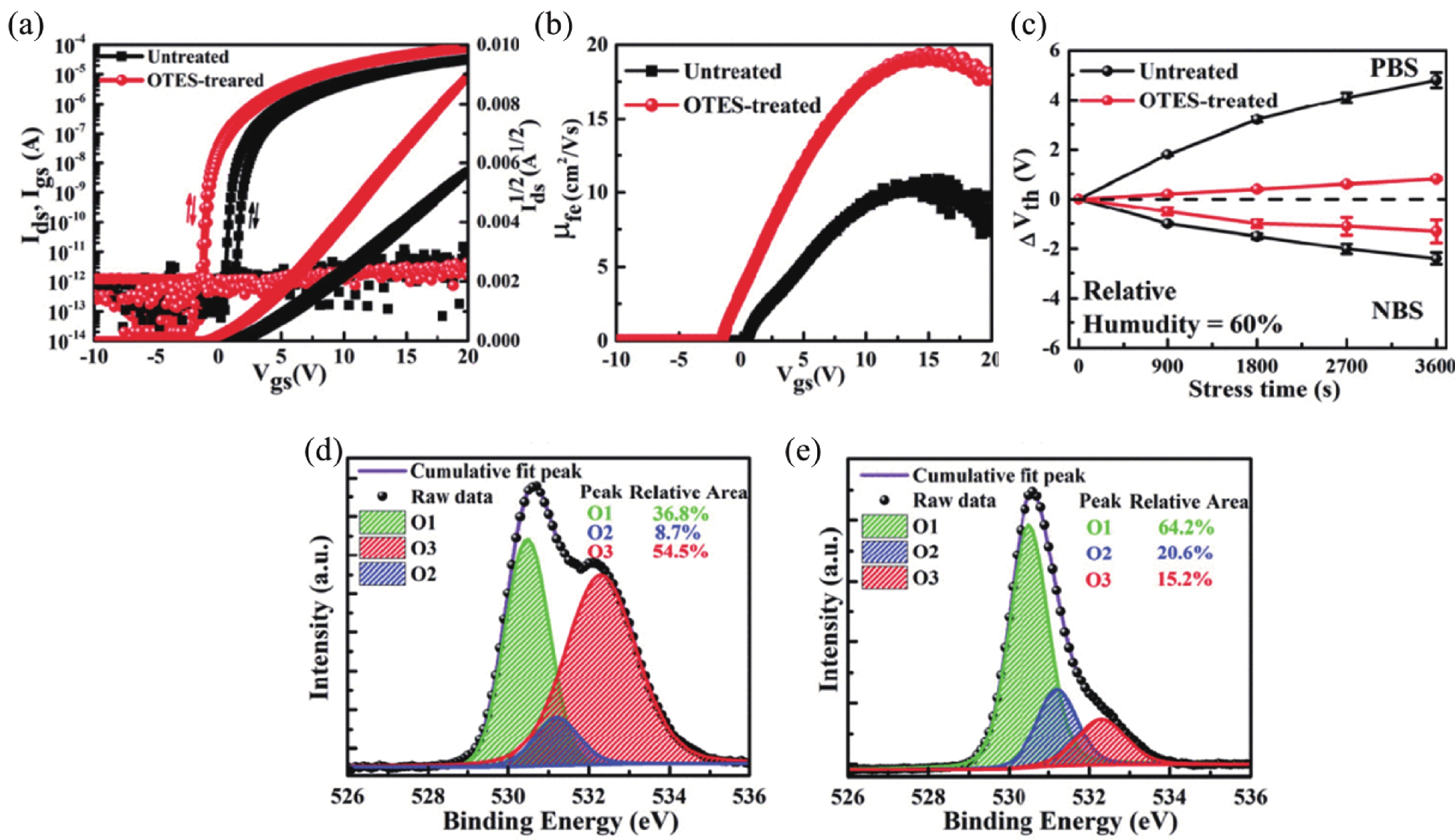
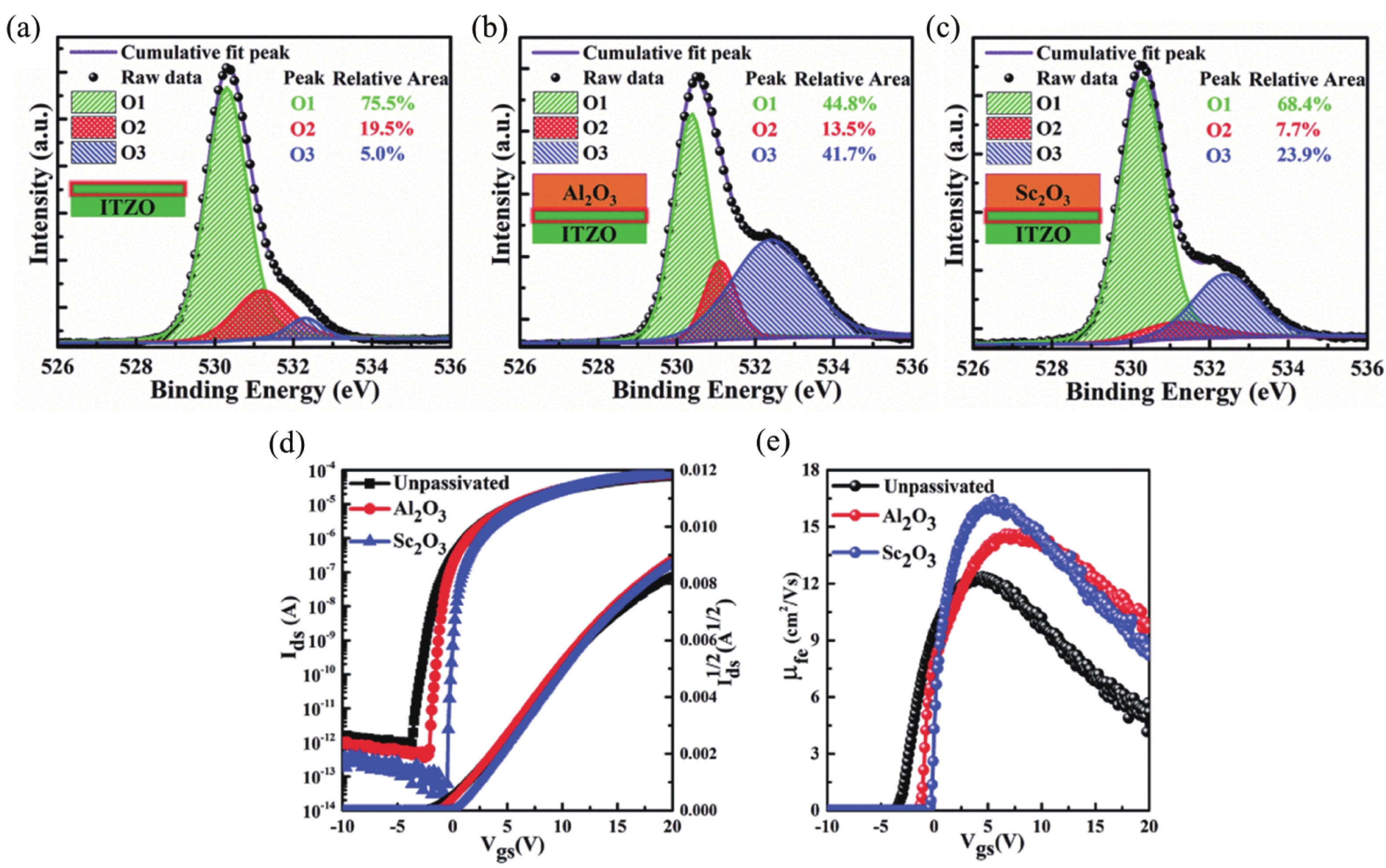

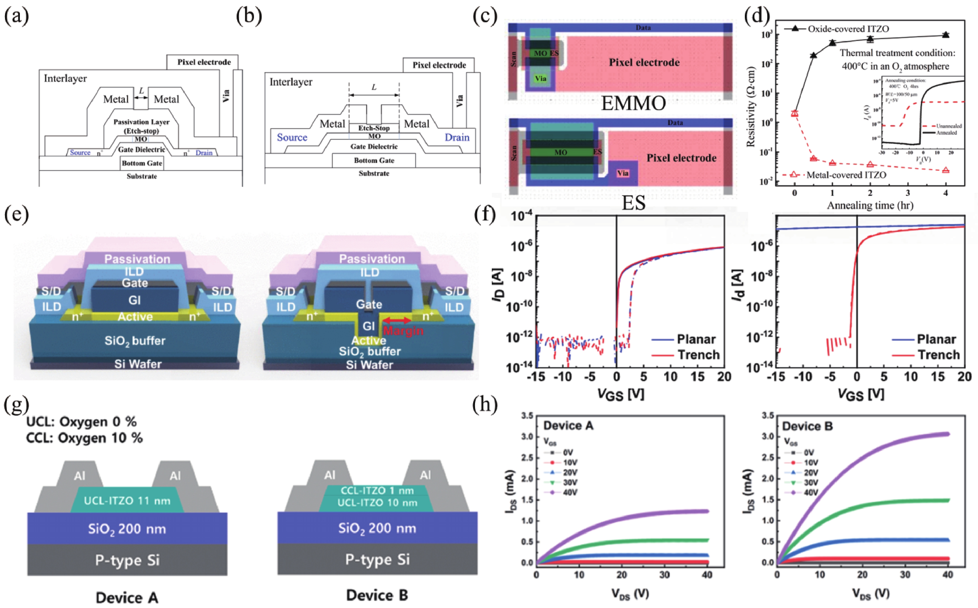
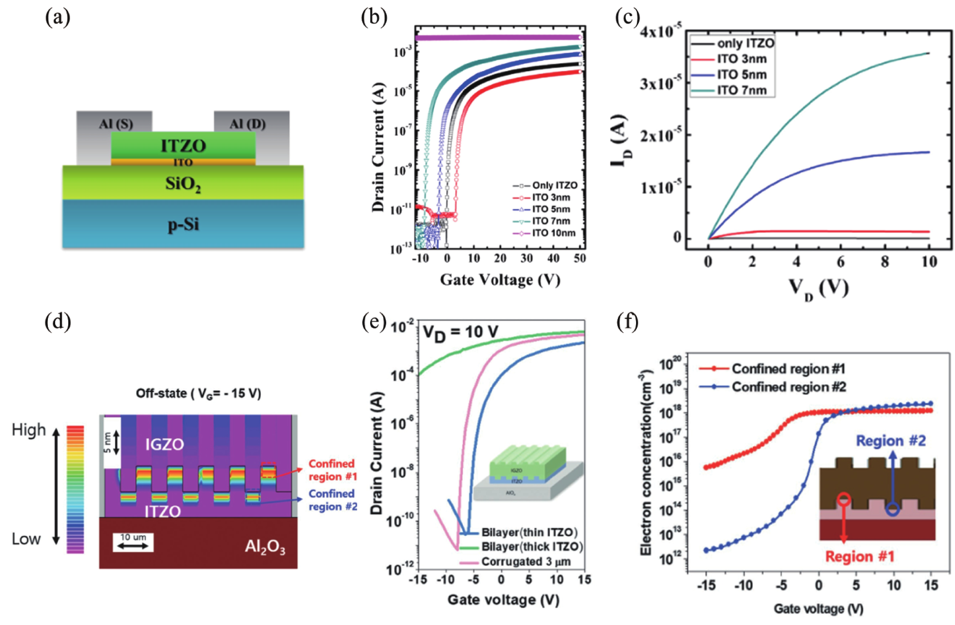
Table 1. Summary of active layer optimizations for ITZO TFTs.
| Methods | Material | W/L (μm) | T (°C) | μ (cm2/(V·s)) | SS (V/dec) | VTH (V) | Year | Ref. | |
| AC film preparation |
Sputtering | ITZO | 150/25 | 350 | 37.2 | 0.93 | N.A. | 2013 | [38] |
| Sputtering | ITZO | 500/50 | 350 | 36.9 | 0.30 | 3.8 | 2014 | [39] | |
| Sputtering | ITZO | 500/100 | 350 | 47.3 | 1.26 | −0.6 | 2018 | [40] | |
| Sputtering | ITZO | 800/400 | 350 | 36.1 | 0.13 | −0.03 | 2021 | [41] | |
| Sputtering | ITZO | 1000/200 | 300 | 30.8 | 1.00 | 0.4 | 2015 | [42] | |
| Sputtering | ITZO | 50/5 | 300 | 27.9 | 0.20 | 0.52 | 2017 | [43] | |
| Inkjet printing | ITZO | 1400/200 | 600 | 30.0 | N.A. | 2.0 | 2009 | [44] | |
| Solution | ITZO | 200/1000 | 600 | 4.36 | 0.53 | 2.1 | 2011 | [45] | |
| Solution | ITZO | 20/10 | 300 | 9.5 | 0.08 | 0.51 | 2019 | [46] | |
| ALD | ITZO | 40/20 | 350 | 27.8 | 0.28 | −1.2 | 2019 | [47] | |
| ALD | ITZO | N.A. | 400 | 22.0 | 0.15 | 0.8 | 2019 | [48] | |
| USPD | ITZO | 200/15 | N.A. | 43.84 | 0.09 | 0.5 | 2020 | [49] | |
| Doping | Sputtering | ITZO:Li | 70/70 | 325 | 39.1 | N.A. | 0.4 | 2018 | [50] |
| Sputtering | ITZO:Li | N.A. | 325 | 39.4 | N.A. | 2.2 | 2019 | [51] | |
| Sputtering | ITZO:Y | 1000/100 | 500 | 0.20 | 0.07 | 3.7 | 2019 | [52] | |
| Sputtering | ITZO:Pr | 800/400 | 350 | 20.9 | 0.27 | 0.39 | 2022 | [53] | |
| Sputtering | ITZO:N | 1500/150 | 250 | 17.53 | 0.36 | −8.2 | 2018 | [55] | |
| Post treatment |
Sputtering | ITZO | N.A. | 400 | 39.6 | 0.25 | −2.8 | 2014 | [56] |
| Sputtering | ITZO | 300/300 | 300 | 27.4 | 0.23 | −0.64 | 2018 | [57] | |
| Sputtering | ITZO | 1000/50 | 150 | 9.8 | 0.82 | 1.93 | 2020 | [58] | |
| Sputtering | ITZO | 1000/500 | 700 | 33.6 | 0.26 | 0.83 | 2020 | [59] | |
| Sputtering | ITZO | 800/600 | 400 | 53.2 | 0.18 | −0.21 | 2021 | [60] | |
| Sputtering | ITZO | 60/50 | 300 | 83.2 | 0.15 | 0.14 | 2023 | [61] |
 DownLoad: CSV
Table 2. Summary of gate dielectric engineering for ITZO TFTs.
| Methods | Dielectric | W/L (μm) | T (°C) | μ (cm2/(V·s)) | SS (V/dec) | VTH (V) | Year | Ref. |
| Sputtering | HfO2 | 480/120 | 400 | 18.9 | 0.48 | −4.64 | 2022 | [64] |
| Sputtering | Al2O3 | 50/50 | 350 | 17.1 | 0.15 | N.A. | 2013 | [65] |
| Sputtering | Al2O3 | 200/200 | 250 | 31.08 | 0.096 | 0.28 | 2016 | [66] |
| Sputtering | ZrO2 | 500/50 | 300 | 40.7 | 0.126 | −0.05 | 2018 | [68] |
| Solution process | ZrO2 | 50/10 | 300 | 15.42 | 0.087 | N.A. | 2018 | [69] |
| Solution process | HZO | 50/10 | 300 | 4.76 | 0.07 | N.A. | 2018 | [70] |
| Sputtering | ZrSiOx | 40/20 | 350 | 28.6 | 0.15 | −0.4 | 2019 | [71] |
| Sputtering | ZS8 | 40/20 | N.A. | 27.7 | 0.17 | −1.1 | 2020 | [72] |
| Sputtering | C8-SAM/Al2O3 | 300/300 | 300 | 13.7 | 0.2 | 1.0 | 2022 | [73] |
DownLoad: CSV
Table 3. Summary of backchannel interface optimization for ITZO TFTs.
| Methods | Dielectric | Passivation | W/L (μm) | T (°C) | μ (cm2/(V·s)) | SS (V/dec) | VTH (V) | Year | Ref. |
| Sputtering | AlOx:Nd | C18-SAM | 300/300 | 300 | 22.9 | 0.077 | −0.1 | 2018 | [77] |
| Sputtering | AlOx:Nd | OTES SAMs | 300/300 | 300 | 19.4 | 0.09 | 0.6 | 2020 | [78] |
| Sputtering | AlOx:Nd | ODA SAMs | 300/300 | 350 | 19.89 | 0.152 | −0.6 | 2021 | [79] |
| Solution process | ZrO2 | Y2O3 | 50/5 | 350 | 4.75 | 0.114 | 0.42 | 2016 | [80] |
| Sputtering | AlOx:Nd | Sc2O3 | 300/300 | 300 | 16.4 | 0.09 | 1.0 | 2021 | [81] |
| Sputtering | SiO2 | GaOx | 60/30 | 400 | 58.3 | 0.087 | −0.7 | 2022 | [82] |
| Sputtering | SiO2 | N.A. | 60/30 | 400 | ~50 | N.A. | N.A. | 2021 | [83] |
DownLoad: CSV
| [1] |
Hirao T, Furuta M, Furuta H, et al. Novel top-gate zinc oxide thin-film transistors (ZnO TFTs) for AMLCDs. Journal of the Society for Information Display, 2007, 15, 17. doi: 10.1889/1.2451545
|
| [2] |
Stewart M, Howell R S, Pires L, et al. Polysilicon TFT technology for active matrix OLED displays. IEEE Trans Electron Devices, 2001, 48, 845 doi: 10.1109/16.918227
|
| [3] |
Sheraw C D, Zhou L, Huang J R, et al. Organic thin-film transistor-driven polymer-dispersed liquid crystal displays on flexible polymeric substrates. Appl Phys Lett, 2002, 80, 1088 doi: 10.1063/1.1448659
|
| [4] |
Kwon J Y, Son K S, Jung J S, et al. Bottom-gate gallium indium zinc oxide thin-film transistor array for high-resolution AMOLED display. IEEE Electron Device Lett, 2008, 29, 1309 doi: 10.1109/LED.2008.2006637
|
| [5] |
Nathan A, Kumar A, Sakariya K, et al. Amorphous silicon thin film transistor circuit integration for organic LED displays on glass and plastic. IEEE J Solid State Circuits, 2004, 39, 1477 doi: 10.1109/JSSC.2004.829373
|
| [6] |
Weimer P K. The TFT A new thin-film transistor. Proc IRE, 1962, 50, 1462 doi: 10.1109/JRPROC.1962.288190
|
| [7] |
Luan S W, Neudeck G W. An experimental study of the source/drain parasitic resistance effects in amorphous silicon thin film transistors. J Appl Phys, 1992, 72, 766 doi: 10.1063/1.351809
|
| [8] |
Sera K, Okumura F, Uchida H, et al. High-performance TFTs fabricated by XeCl excimer laser annealing of hydrogenated amorphous-silicon film. IEEE Trans Electron Devices, 1989, 36, 2868 doi: 10.1109/16.40970
|
| [9] |
Kuriyama H, Kiyama S, Noguchi S, et al. Enlargement of poly-Si film grain size by excimer laser annealing and its application to high-performance poly-Si thin film transistor. Jpn J Appl Phys, 1991, 30, 3700 doi: 10.1143/JJAP.30.3700
|
| [10] |
Brotherton S D. Polycrystalline silicon thin film transistors. Semicond Sci Technol, 1995, 10, 721 doi: 10.1088/0268-1242/10/6/001
|
| [11] |
Meng Z G, Wang M X, Wong M. High performance low temperature metal-induced unilaterally crystallized polycrystalline silicon thin film transistors for system-on-panel applications. IEEE Trans Electron Devices, 2000, 47, 404 doi: 10.1109/16.822287
|
| [12] |
Zhao X F, Wen D Z, Zhuang C C, et al. Fabrication and characteristics of magnetic field sensors based on nano-polysilicon thin-film transistors. J Semicond, 2013, 34, 036001 doi: 10.1088/1674-4926/34/3/036001
|
| [13] |
Cai W S, Li H Y, Li M C, et al. Performance enhancement of solution-processed InZnO thin-film transistors by Al doping and surface passivation. J Semicond, 2022, 43, 034102 doi: 10.1088/1674-4926/43/3/034102
|
| [14] |
Liang Y Y, Kyungsoo J, Velumani S, et al. Effects of interface trap density on the electrical performance of amorphous InSnZnO thin-film transistor. J Semicond, 2015, 36, 024007 doi: 10.1088/1674-4926/36/2/024007
|
| [15] |
Zhu X M, Wu H Z, Wang S J, et al. Optical and electrical properties of N-doped ZnO and fabrication of thin-film transistors. J Semicond, 2009, 30, 033001 doi: 10.1088/1674-4926/30/3/033001
|
| [16] |
Zhu Y, He Y L, Jiang S S, et al. Indium–gallium–zinc–oxide thin-film transistors: Materials, devices, and applications. J Semicond, 2021, 42, 031101 doi: 10.1088/1674-4926/42/3/031101
|
| [17] |
Mittal P, Negi Y S, Singh R K. Impact of source and drain contact thickness on the performance of organic thin film transistors. J Semicond, 2014, 35, 124002 doi: 10.1088/1674-4926/35/12/124002
|
| [18] |
Li Z F, Luo X Y. ADO-phosphonic acid self-assembled monolayer modified dielectrics for organic thin film transistors. J Semicond, 2014, 35, 104004 doi: 10.1088/1674-4926/35/10/104004
|
| [19] |
Lin C L, Cheng M H, Tu C D, et al. Highly reliable integrated gate driver circuit for large TFT-LCD applications. IEEE Electron Device Lett, 2012, 33, 679 doi: 10.1109/LED.2012.2188269
|
| [20] |
Liao C W, He C D, Chen T, et al. Design of integrated amorphous-silicon thin-film transistor gate driver. J Disp Technol, 2013, 9, 7 doi: 10.1109/JDT.2012.2221154
|
| [21] |
Lin C L, Tu C D, Chuang M C, et al. Design of bidirectional and highly stable integrated hydrogenated amorphous silicon gate driver circuits. J Disp Technol, 2011, 7, 10 doi: 10.1109/JDT.2010.2085077
|
| [22] |
Tanaka T, Asuma H, Ogawa K, et al. An LCD addressed by a-Si: H TFTs with peripheral poly-Si TFT circuits. Proceedings of IEEE International Electron Devices Meeting. Washington, DC, USA. IEEE, 2002, 389 doi: 10.1109/IEDM.1993.347327
|
| [23] |
Nomura K, Ohta H, Takagi A, et al. Room-temperature fabrication of transparent flexible thin-film transistors using amorphous oxide semiconductors. Nature, 2004, 432, 488 doi: 10.1038/nature03090
|
| [24] |
Son K S, Kim T S, Jung J S, et al. 4 inch QVGA AMOLED driven by the threshold voltage controlled amorphous GIZO (Ga2O3-In2O3-ZnO) TFT. SID Symp Dig Tech Pap, 2008, 39, 633 doi: 10.1889/1.3069743
|
| [25] |
Lee J H, Kim D H, Yang D J, et al. World’s largest (15-inch) XGA AMLCD panel using IGZO oxide TFT. SID Symp Dig Tech Pap, 2008, 39, 625 doi: 10.1889/1.3069740
|
| [26] |
Park J S, Kim T W, Stryakhilev D, et al. Flexible full color organic light-emitting diode display on polyimide plastic substrate driven by amorphous indium gallium zinc oxide thin-film transistors. Appl Phys Lett, 2009, 95, 013503 doi: 10.1063/1.3159832
|
| [27] |
Park J S, Lim J H. 4-3: Invited paper: High mobility oxide thin-film transistors for AMOLED displays. SID Symp Dig Tech Pap, 2022, 53, 20 doi: https://doi.org/10.1002/sdtp.15405
|
| [28] |
Arai T. Oxide-TFT technologies for next-generation AMOLED displays. J Soc Inf Disp, 2012, 20, 156 doi: 10.1889/JSID20.3.156
|
| [29] |
Lin C L, Lai P C, Lai P C, et al. Pixel circuit with parallel driving scheme for compensating luminance variation based on a-IGZO TFT for AMOLED displays. J Disp Technol, 2016, 12, 1681 doi: 10.1109/JDT.2016.2616507
|
| [30] |
Chen Y F, Lee S H, Kim H, et al. In-pixel temperature sensor for high-luminance active matrix micro-light-emitting diode display using low-temperature polycrystalline silicon and oxide thin-film-transistors. J Soc Inf Disp, 2020, 28, 528 doi: 10.1002/jsid.915
|
| [31] |
Cho D, Moon J, Kihm T Y, et al. 48-4: LTPO technology development for enhanced display performance: Image sticking phenomena, circuit operation and backplane process integration. SID Symp Dig Tech Pap, 2022, 53, 620 doi: 10.1002/sdtp.15564
|
| [32] |
Shiah Y S, Sim K, Shi Y H, et al. Mobility–stability trade-off in oxide thin-film transistors. Nat Electron, 2021, 4, 800 doi: 10.1038/s41928-021-00671-0
|
| [33] |
Shi J L, Zhang J Y, Yang L, et al. Wide bandgap oxide semiconductors: From materials physics to optoelectronic devices. Adv Mater, 2021, 33, 2006230 doi: 10.1002/adma.202006230
|
| [34] |
Noh J Y, Kim H, Nahm H H, et al. Cation composition effects on electronic structures of In-Sn-Zn-O amorphous semiconductors. J Appl Phys, 2013, 113, 183706 doi: 10.1063/1.4803706
|
| [35] |
Fortunato E, Barquinha P, Martins R. Oxide semiconductor thin-film transistors: A review of recent advances. Adv Mater, 2012, 24, 2945 doi: 10.1002/adma.201103228
|
| [36] |
Wallmark J, Johnson H. Field-effect transistors: Physics, technology and applications. Prentice-Hall, 1966
|
| [37] |
Petti L, Münzenrieder N, Vogt C, et al. Metal oxide semiconductor thin-film transistors for flexible electronics. Appl Phys Rev, 2016, 3, 021303 doi: 10.1063/1.4953034
|
| [38] |
Jang K, Raja J, Lee Y J, et al. Effects of carrier concentration, indium content, and crystallinity on the electrical properties of indium-tin-zinc-oxide thin-film transistors. IEEE Electron Device Lett, 2013, 34, 1151 doi: 10.1109/LED.2013.2272084
|
| [39] |
Kim S H, Ahn C H, Yun M G, et al. Anomalous tin chemical bonding in indium-zinc-tin oxide films and their thin film transistor performance. J Phys D: Appl Phys, 2014, 47, 485101 doi: 10.1088/0022-3727/47/48/485101
|
| [40] |
Park J, Rim Y S, Li C, et al. Defect-induced instability mechanisms of sputtered amorphous indium tin zinc oxide thin-film transistors. J Appl Phys, 2018, 123, 161568 doi: 10.1063/1.5004148
|
| [41] |
Wu Z D, Zhang H B, Wang X L, et al. Effects of target quality on electrical performance and stability of In-Sn-Zn-O thin-film transistors. IEEE Electron Device Lett, 2021, 42, 529 doi: 10.1109/LED.2021.3062369
|
| [42] |
Jia J J, Torigoshi Y, Kawashima E, et al. Amorphous indium-tin-zinc oxide films deposited by magnetron sputtering with various reactive gases: Spatial distribution of thin film transistor performance. Appl Phys Lett, 2015, 106, 023502 doi: 10.1063/1.4905654
|
| [43] |
Pan T M, Peng B J, Her J L, et al. Effect of in and Zn content on structural and electrical properties of InZnSnO thin-film transistors using an Yb2TiO5 gate dielectric. IEEE Trans Electron Devices, 2017, 64, 2233 doi: 10.1109/TED.2017.2680410
|
| [44] |
Lee D H, Han S Y, Herman G S, et al. Inkjet printed high-mobility indium zinc tin oxide thin film transistors. J Mater Chem, 2009, 19, 3135 doi: 10.1039/b822893k
|
| [45] |
Kim B J, Kim H J, Yoon T S, et al. Solution processed IZTO thin film transistor on silicon nitride dielectric layer. J Ind Eng Chem, 2011, 17, 96 doi: 10.1016/j.jiec.2010.12.003
|
| [46] |
Bukke R N, Mude N N, Saha J K, et al. High performance of a-IZTO TFT by purification of the semiconductor oxide precursor. Adv Mater Interfaces, 2019, 6, 1900277 doi: 10.1002/admi.201900277
|
| [47] |
Sheng J Z, Hong T, Kang D, et al. Design of InZnSnO semiconductor alloys synthesized by supercycle atomic layer deposition and their rollable applications. ACS Appl Mater Interfaces, 2019, 11, 12683 doi: 10.1021/acsami.9b02999
|
| [48] |
Baek I H, Pyeon J J, Han S H, et al. High-performance thin-film transistors of quaternary indium–zinc–tin oxide films grown by atomic layer deposition. ACS Appl Mater Interfaces, 2019, 11, 14892 doi: 10.1021/acsami.9b03331
|
| [49] |
Liu H Y, Hsu W C, Chen J H, et al. Amorphous ITZO thin-film transistors by using ultrasonic spray pyrolysis deposition. IEEE Trans Electron Devices, 2020, 67, 1009 doi: 10.1109/TED.2020.2965949
|
| [50] |
Li R, Dai S Q, Ma Y B, et al. High-performance transparent Li-doped indium-tin-zinc-oxide thin film transistor fabricated by radio frequency magnetron sputtering method. Mater Lett, 2018, 230, 132 doi: 10.1016/j.matlet.2018.07.098
|
| [51] |
Li R, Dai S Q, Su J B, et al. Effect of thermal annealing on the electrical characteristics of an amorphous ITZO: Li thin film transistor fabricated using the magnetron sputtering method. Mater Sci Semicond Process, 2019, 96, 8 doi: 10.1016/j.mssp.2019.02.005
|
| [52] |
Zhang Y P, Zhang H, Yang J, et al. Solution-processed yttrium-doped IZTO semiconductors for high-stability thin film transistor applications. IEEE Trans Electron Devices, 2019, 66, 5170 doi: 10.1109/TED.2019.2949702
|
| [53] |
Zhang H B, Liang L Y, Wang X L, et al. Praseodymium-doped In-Sn-Zn-O TFTs with effective improvement of negative-bias illumination stress stability. IEEE Trans Electron Devices, 2022, 69, 152 doi: 10.1109/TED.2021.3126278
|
| [54] |
Jia J J, Torigoshi Y, Suko A, et al. Effect of nitrogen addition on the structural, electrical, and optical properties of In-Sn-Zn oxide thin films. Appl Surf Sci, 2017, 396, 897 doi: 10.1016/j.apsusc.2016.11.058
|
| [55] |
Li Z Y, Yang H Z, Chen S C, et al. Impact of active layer thickness of nitrogen-doped In–Sn–Zn–O films on materials and thin film transistor performances. J Phys D: Appl Phys, 2018, 51, 175101 doi: 10.1088/1361-6463/aab7db
|
| [56] |
Fuh C S, Liu P T, Huang W H, et al. Effect of annealing on defect elimination for high mobility amorphous indium-zinc-tin-oxide thin-film transistor. IEEE Electron Device Lett, 2014, 35, 1103 doi: 10.1109/LED.2014.2354598
|
| [57] |
Zhong W, Li G Y, Lan L F, et al. Effects of annealing temperature on properties of InSnZnO thin film transistors prepared by Co-sputtering. RSC Adv, 2018, 8, 34817 doi: 10.1039/C8RA06692B
|
| [58] |
Maeng S, Kim H, Choi G, et al. Investigation of electrical performance and operation stability of RF-sputtered InSnZnO thin film transistors by oxygen-ambient rapid thermal annealing. Semicond Sci Technol, 2020, 35, 125019 doi: 10.1088/1361-6641/abbc8f
|
| [59] |
Park S, Park K, Kim H, et al. Light-induced bias stability of crystalline indium-tin-zinc-oxide thin film transistors. Appl Surf Sci, 2020, 526, 146655 doi: 10.1016/j.apsusc.2020.146655
|
| [60] |
Wang X L, Liang L Y, Zhang H B, et al. Huge mobility enhancement of InSnZnO thin-film transistors via Al-induced microstructure regularization. Appl Phys Lett, 2021, 119, 212102 doi: 10.1063/5.0072077
|
| [61] |
Kim G B, On N, Kim T, et al. High mobility IZTO thin-film transistors based on spinel phase formation at low temperature through a catalytic chemical reaction. Small Methods, 2023, 2201522 doi: 10.1002/smtd.202201522
|
| [62] |
Tseng W H, Fang S W, Lu C Y, et al. The effect of nitrous oxide plasma treatment on the bias temperature stress of metal oxide thin film transistors with high mobility. Solid State Electron, 2015, 103, 173 doi: 10.1016/j.sse.2014.07.017
|
| [63] |
Wang B H, Huang W, Chi L F, et al. High- k gate dielectrics for emerging flexible and stretchable electronics. Chem Rev, 2018, 118, 5690 doi: 10.1021/acs.chemrev.8b00045
|
| [64] |
Bak Y G, Park J W, Park Y J, et al. In-Zn-Sn-O thin film based transistor with high-k HfO2 dielectric. Thin Solid Films, 2022, 753, 139290 doi: 10.1016/j.tsf.2022.139290
|
| [65] |
Jang K, Raja J, Kim J, et al. Bias-stability improvement using Al2O3 interfacial dielectrics in a-InSnZnO thin-film transistors. Semicond Sci Technol, 2013, 28, 085015 doi: 10.1088/0268-1242/28/8/085015
|
| [66] |
Raja J, Nguyen C P T, Lee C M, et al. Improved data retention of InSnZnO nonvolatile memory by H2O2 treated Al2O3 tunneling layer: A cost-effective method. IEEE Electron Device Lett, 2016, 37, 1272 doi: 10.1109/LED.2016.2599559
|
| [67] |
Javey A, Kim H, Brink M, et al. High-κ dielectrics for advanced carbon-nanotube transistors and logic gates. Nat Mater, 2002, 1, 241 doi: 10.1038/nmat769
|
| [68] |
Ruan D B, Liu P T, Chiu Y C, et al. Investigation of low operation voltage InZnSnO thin-film transistors with different high-k gate dielectric by physical vapor deposition. Thin Solid Films, 2018, 660, 885 doi: 10.1016/j.tsf.2018.02.036
|
| [69] |
Bukke R N, Avis C, Naik M N, et al. Remarkable increase in field effect mobility of amorphous IZTO thin-film transistors with purified ZrOx gate insulator. IEEE Electron Device Lett, 2018, 39, 371 doi: 10.1109/LED.2018.2791633
|
| [70] |
Bukke R N, Naik Mude N, Lee J, et al. Effect of Hf alloy in ZrOx gate insulator for solution processed a-IZTO thin film transistors. IEEE Electron Device Lett, 2019, 40, 32 doi: 10.1109/LED.2018.2880177
|
| [71] |
Kim M, Jeong H J, Sheng J Z, et al. The impact of plasma-enhanced atomic layer deposited ZrSiOx insulators on low voltage operated In-Sn-Zn-O thin film transistors. Ceram Int, 2019, 45, 19166 doi: 10.1016/j.ceramint.2019.06.163
|
| [72] |
Choi W H, Jeon W, Park J S. Nanoscale surface engineering of a high- k ZrO2/SiO2 gate insulator for a high performance ITZO TFT via plasma-enhanced atomic layer deposition. J Mater Chem C, 2020, 8, 13342 doi: 10.1039/D0TC02419H
|
| [73] |
Zhong W, Zhang J F, Liu Y, et al. Gate dielectric treated by self-assembled monolayers (SAMs) to enhance the performance of InSnZnO thin-film transistors. IEEE Trans Electron Devices, 2022, 69, 2398 doi: 10.1109/TED.2022.3155709
|
| [74] |
Nguyen C P T, Trinh T T, Raja J, et al. Source/drain metallization effects on the specific contact resistance of indium tin zinc oxide thin film transistors. Mater Sci Semicond Process, 2015, 39, 649 doi: 10.1016/j.mssp.2015.05.069
|
| [75] |
Park J, Shin M, Yi J. Comparative study of aluminum and nickel contact electrodes for indium–tin–zinc oxide thin film transistors using oxygen vacancy diffusion model. Mater Sci Semicond Process, 2020, 120, 105253 doi: 10.1016/j.mssp.2020.105253
|
| [76] |
Cho S H, Lee Y U, Lee J S, et al. Effect of self-assembled monolayer (SAM) on the oxide semiconductor thin film transistor. J Disp Technol, 2012, 8, 35 doi: 10.1109/JDT.2011.2169936
|
| [77] |
Zhong W, Li G Y, Lan L F, et al. InSnZnO thin-film transistors with vapor- phase self-assembled monolayer as passivation layer. IEEE Electron Device Lett, 2018, 39, 1680 doi: 10.1109/LED.2018.2872352
|
| [78] |
Zhong W, Yao R H, Liu Y, et al. Effect of self-assembled monolayers (SAMs) as surface passivation on the flexible a-InSnZnO thin-film transistors. IEEE Trans Electron Devices, 2020, 67, 3157 doi: 10.1109/TED.2020.3004420
|
| [79] |
Chen Y Y, Li B, Zhong W, et al. InSnZnO thin-film transistors with nitrogenous self-assembled multilayers passivation. IEEE Trans Electron Devices, 2021, 68, 5612 doi: 10.1109/TED.2021.3114267
|
| [80] |
Bukke R N, Avis C, Jang J. Solution-processed amorphous In–Zn–Sn oxide thin-film transistor performance improvement by solution-processed Y2O3 passivation. IEEE Electron Device Lett, 2016, 37, 433 doi: 10.1109/LED.2016.2528288
|
| [81] |
Zhong W, Kang L Y, Deng S B, et al. Effect of Sc2O3 passivation layer on the electrical characteristics and stability of InSnZnO thin-film transistors. IEEE Trans Electron Devices, 2021, 68, 4956 doi: 10.1109/TED.2021.3105486
|
| [82] |
Shi Y H, Shiah Y S, Sim K, et al. High-performance a-ITZO TFTs with high bias stability enabled by self-aligned passivation using a-GaOx. Appl Phys Lett, 2022, 121, 212101 doi: 10.1063/5.0123253
|
| [83] |
Shiah Y S, Sim K, Ueda S, et al. Unintended carbon-related impurity and negative bias instability in high-mobility oxide TFTs. IEEE Electron Device Lett, 2021, 42, 1319 doi: 10.1109/LED.2021.3101654
|
| [84] |
Jeon G J, Yang J, Lee S H, et al. Abnormal thermal instability of Al-InSnZnO thin-film transistor by hydroxyl-induced oxygen vacancy at SiOx/active interface. IEEE Electron Device Lett, 2021, 42, 363 doi: 10.1109/LED.2021.3054859
|
| [85] |
Xia Z H, Lu L, Li J P, et al. Characteristics of elevated-metal metal-oxide thin-film transistors based on indium-tin-zinc oxide. IEEE Electron Device Lett, 2017, 38, 894 doi: 10.1109/LED.2017.2707090
|
| [86] |
Kim J, Kim D H, Cho S I, et al. Channel-shortening effect suppression of a high-mobility self-aligned oxide TFT using trench structure. IEEE Electron Device Lett, 2021, 42, 1798 doi: 10.1109/LED.2021.3125146
|
| [87] |
Lee J, Jin J D, Maeng S, et al. Enhancement of the electrical performance and bias stability of RF-sputtered indium tin zinc oxide thin-film transistors with vertical stoichiometric oxygen control. ACS Appl Electron Mater, 2022, 4, 1800 doi: 10.1021/acsaelm.2c00054
|
| [88] |
Jin J D, Lin X Y, Zhang J W, et al. Low-voltage, high-performance, indium-tin-zinc-oxide thin-film transistors based on dual-channel and anodic-oxide. Adv Electron Mater, 2023, 9, 2201117 doi: 10.1002/aelm.202201117
|
| [89] |
Nguyen C P T, Raja J, Kim S, et al. Enhanced electrical properties of oxide semiconductor thin-film transistors with high conductivity thin layer insertion for the channel region. Appl Surf Sci, 2017, 396, 1472 doi: 10.1016/j.apsusc.2016.11.194
|
| [90] |
Lee M, Jo J W, Kim Y J, et al. Corrugated heterojunction metal-oxide thin-film transistors with high electron mobility via vertical interface manipulation. Adv Mater, 2018, 30, 1804120 doi: 10.1002/adma.201804120
|
| [91] |
Yu W, Zhao D Y, Cai J, et al. Performance enhancement of TiZO thin film transistors by introducing a thin ITO interlayer. IEEE J Electron Devices Soc, 2019, 7, 1302 doi: 10.1109/JEDS.2019.2951738
|


Article views: 1031 Times PDF downloads: 178 Times Cited by: 0 Times
Received: 11 May 2023 Revised: 29 May 2023 Online: Accepted Manuscript: 16 August 2023Corrected proof: 18 August 2023Uncorrected proof: 21 August 2023Published: 10 September 2023
| Citation: |
Feilian Chen, Meng Zhang, Yunhao Wan, Xindi Xu, Man Wong, Hoi-Sing Kwok. Advances in mobility enhancement of ITZO thin-film transistors: a review[J]. Journal of Semiconductors, 2023, 44(9): 091602. doi: 10.1088/1674-4926/44/9/091602
F L Chen, M Zhang, Y H Wan, X D Xu, M Wong, H S Kwok. Advances in mobility enhancement of ITZO thin-film transistors: a review[J]. J. Semicond, 2023, 44(9): 091602. doi: 10.1088/1674-4926/44/9/091602
Export: BibTex EndNote

|
| [1] |
Hirao T, Furuta M, Furuta H, et al. Novel top-gate zinc oxide thin-film transistors (ZnO TFTs) for AMLCDs. Journal of the Society for Information Display, 2007, 15, 17. doi: 10.1889/1.2451545
|
| [2] |
Stewart M, Howell R S, Pires L, et al. Polysilicon TFT technology for active matrix OLED displays. IEEE Trans Electron Devices, 2001, 48, 845 doi: 10.1109/16.918227
|
| [3] |
Sheraw C D, Zhou L, Huang J R, et al. Organic thin-film transistor-driven polymer-dispersed liquid crystal displays on flexible polymeric substrates. Appl Phys Lett, 2002, 80, 1088 doi: 10.1063/1.1448659
|
| [4] |
Kwon J Y, Son K S, Jung J S, et al. Bottom-gate gallium indium zinc oxide thin-film transistor array for high-resolution AMOLED display. IEEE Electron Device Lett, 2008, 29, 1309 doi: 10.1109/LED.2008.2006637
|
| [5] |
Nathan A, Kumar A, Sakariya K, et al. Amorphous silicon thin film transistor circuit integration for organic LED displays on glass and plastic. IEEE J Solid State Circuits, 2004, 39, 1477 doi: 10.1109/JSSC.2004.829373
|
| [6] |
Weimer P K. The TFT A new thin-film transistor. Proc IRE, 1962, 50, 1462 doi: 10.1109/JRPROC.1962.288190
|
| [7] |
Luan S W, Neudeck G W. An experimental study of the source/drain parasitic resistance effects in amorphous silicon thin film transistors. J Appl Phys, 1992, 72, 766 doi: 10.1063/1.351809
|
| [8] |
Sera K, Okumura F, Uchida H, et al. High-performance TFTs fabricated by XeCl excimer laser annealing of hydrogenated amorphous-silicon film. IEEE Trans Electron Devices, 1989, 36, 2868 doi: 10.1109/16.40970
|
| [9] |
Kuriyama H, Kiyama S, Noguchi S, et al. Enlargement of poly-Si film grain size by excimer laser annealing and its application to high-performance poly-Si thin film transistor. Jpn J Appl Phys, 1991, 30, 3700 doi: 10.1143/JJAP.30.3700
|
| [10] |
Brotherton S D. Polycrystalline silicon thin film transistors. Semicond Sci Technol, 1995, 10, 721 doi: 10.1088/0268-1242/10/6/001
|
| [11] |
Meng Z G, Wang M X, Wong M. High performance low temperature metal-induced unilaterally crystallized polycrystalline silicon thin film transistors for system-on-panel applications. IEEE Trans Electron Devices, 2000, 47, 404 doi: 10.1109/16.822287
|
| [12] |
Zhao X F, Wen D Z, Zhuang C C, et al. Fabrication and characteristics of magnetic field sensors based on nano-polysilicon thin-film transistors. J Semicond, 2013, 34, 036001 doi: 10.1088/1674-4926/34/3/036001
|
| [13] |
Cai W S, Li H Y, Li M C, et al. Performance enhancement of solution-processed InZnO thin-film transistors by Al doping and surface passivation. J Semicond, 2022, 43, 034102 doi: 10.1088/1674-4926/43/3/034102
|
| [14] |
Liang Y Y, Kyungsoo J, Velumani S, et al. Effects of interface trap density on the electrical performance of amorphous InSnZnO thin-film transistor. J Semicond, 2015, 36, 024007 doi: 10.1088/1674-4926/36/2/024007
|
| [15] |
Zhu X M, Wu H Z, Wang S J, et al. Optical and electrical properties of N-doped ZnO and fabrication of thin-film transistors. J Semicond, 2009, 30, 033001 doi: 10.1088/1674-4926/30/3/033001
|
| [16] |
Zhu Y, He Y L, Jiang S S, et al. Indium–gallium–zinc–oxide thin-film transistors: Materials, devices, and applications. J Semicond, 2021, 42, 031101 doi: 10.1088/1674-4926/42/3/031101
|
| [17] |
Mittal P, Negi Y S, Singh R K. Impact of source and drain contact thickness on the performance of organic thin film transistors. J Semicond, 2014, 35, 124002 doi: 10.1088/1674-4926/35/12/124002
|
| [18] |
Li Z F, Luo X Y. ADO-phosphonic acid self-assembled monolayer modified dielectrics for organic thin film transistors. J Semicond, 2014, 35, 104004 doi: 10.1088/1674-4926/35/10/104004
|
| [19] |
Lin C L, Cheng M H, Tu C D, et al. Highly reliable integrated gate driver circuit for large TFT-LCD applications. IEEE Electron Device Lett, 2012, 33, 679 doi: 10.1109/LED.2012.2188269
|
| [20] |
Liao C W, He C D, Chen T, et al. Design of integrated amorphous-silicon thin-film transistor gate driver. J Disp Technol, 2013, 9, 7 doi: 10.1109/JDT.2012.2221154
|
| [21] |
Lin C L, Tu C D, Chuang M C, et al. Design of bidirectional and highly stable integrated hydrogenated amorphous silicon gate driver circuits. J Disp Technol, 2011, 7, 10 doi: 10.1109/JDT.2010.2085077
|
| [22] |
Tanaka T, Asuma H, Ogawa K, et al. An LCD addressed by a-Si: H TFTs with peripheral poly-Si TFT circuits. Proceedings of IEEE International Electron Devices Meeting. Washington, DC, USA. IEEE, 2002, 389 doi: 10.1109/IEDM.1993.347327
|
| [23] |
Nomura K, Ohta H, Takagi A, et al. Room-temperature fabrication of transparent flexible thin-film transistors using amorphous oxide semiconductors. Nature, 2004, 432, 488 doi: 10.1038/nature03090
|
| [24] |
Son K S, Kim T S, Jung J S, et al. 4 inch QVGA AMOLED driven by the threshold voltage controlled amorphous GIZO (Ga2O3-In2O3-ZnO) TFT. SID Symp Dig Tech Pap, 2008, 39, 633 doi: 10.1889/1.3069743
|
| [25] |
Lee J H, Kim D H, Yang D J, et al. World’s largest (15-inch) XGA AMLCD panel using IGZO oxide TFT. SID Symp Dig Tech Pap, 2008, 39, 625 doi: 10.1889/1.3069740
|
| [26] |
Park J S, Kim T W, Stryakhilev D, et al. Flexible full color organic light-emitting diode display on polyimide plastic substrate driven by amorphous indium gallium zinc oxide thin-film transistors. Appl Phys Lett, 2009, 95, 013503 doi: 10.1063/1.3159832
|
| [27] |
Park J S, Lim J H. 4-3: Invited paper: High mobility oxide thin-film transistors for AMOLED displays. SID Symp Dig Tech Pap, 2022, 53, 20 doi: https://doi.org/10.1002/sdtp.15405
|
| [28] |
Arai T. Oxide-TFT technologies for next-generation AMOLED displays. J Soc Inf Disp, 2012, 20, 156 doi: 10.1889/JSID20.3.156
|
| [29] |
Lin C L, Lai P C, Lai P C, et al. Pixel circuit with parallel driving scheme for compensating luminance variation based on a-IGZO TFT for AMOLED displays. J Disp Technol, 2016, 12, 1681 doi: 10.1109/JDT.2016.2616507
|
| [30] |
Chen Y F, Lee S H, Kim H, et al. In-pixel temperature sensor for high-luminance active matrix micro-light-emitting diode display using low-temperature polycrystalline silicon and oxide thin-film-transistors. J Soc Inf Disp, 2020, 28, 528 doi: 10.1002/jsid.915
|
| [31] |
Cho D, Moon J, Kihm T Y, et al. 48-4: LTPO technology development for enhanced display performance: Image sticking phenomena, circuit operation and backplane process integration. SID Symp Dig Tech Pap, 2022, 53, 620 doi: 10.1002/sdtp.15564
|
| [32] |
Shiah Y S, Sim K, Shi Y H, et al. Mobility–stability trade-off in oxide thin-film transistors. Nat Electron, 2021, 4, 800 doi: 10.1038/s41928-021-00671-0
|
| [33] |
Shi J L, Zhang J Y, Yang L, et al. Wide bandgap oxide semiconductors: From materials physics to optoelectronic devices. Adv Mater, 2021, 33, 2006230 doi: 10.1002/adma.202006230
|
| [34] |
Noh J Y, Kim H, Nahm H H, et al. Cation composition effects on electronic structures of In-Sn-Zn-O amorphous semiconductors. J Appl Phys, 2013, 113, 183706 doi: 10.1063/1.4803706
|
| [35] |
Fortunato E, Barquinha P, Martins R. Oxide semiconductor thin-film transistors: A review of recent advances. Adv Mater, 2012, 24, 2945 doi: 10.1002/adma.201103228
|
| [36] |
Wallmark J, Johnson H. Field-effect transistors: Physics, technology and applications. Prentice-Hall, 1966
|
| [37] |
Petti L, Münzenrieder N, Vogt C, et al. Metal oxide semiconductor thin-film transistors for flexible electronics. Appl Phys Rev, 2016, 3, 021303 doi: 10.1063/1.4953034
|
| [38] |
Jang K, Raja J, Lee Y J, et al. Effects of carrier concentration, indium content, and crystallinity on the electrical properties of indium-tin-zinc-oxide thin-film transistors. IEEE Electron Device Lett, 2013, 34, 1151 doi: 10.1109/LED.2013.2272084
|
| [39] |
Kim S H, Ahn C H, Yun M G, et al. Anomalous tin chemical bonding in indium-zinc-tin oxide films and their thin film transistor performance. J Phys D: Appl Phys, 2014, 47, 485101 doi: 10.1088/0022-3727/47/48/485101
|
| [40] |
Park J, Rim Y S, Li C, et al. Defect-induced instability mechanisms of sputtered amorphous indium tin zinc oxide thin-film transistors. J Appl Phys, 2018, 123, 161568 doi: 10.1063/1.5004148
|
| [41] |
Wu Z D, Zhang H B, Wang X L, et al. Effects of target quality on electrical performance and stability of In-Sn-Zn-O thin-film transistors. IEEE Electron Device Lett, 2021, 42, 529 doi: 10.1109/LED.2021.3062369
|
| [42] |
Jia J J, Torigoshi Y, Kawashima E, et al. Amorphous indium-tin-zinc oxide films deposited by magnetron sputtering with various reactive gases: Spatial distribution of thin film transistor performance. Appl Phys Lett, 2015, 106, 023502 doi: 10.1063/1.4905654
|
| [43] |
Pan T M, Peng B J, Her J L, et al. Effect of in and Zn content on structural and electrical properties of InZnSnO thin-film transistors using an Yb2TiO5 gate dielectric. IEEE Trans Electron Devices, 2017, 64, 2233 doi: 10.1109/TED.2017.2680410
|
| [44] |
Lee D H, Han S Y, Herman G S, et al. Inkjet printed high-mobility indium zinc tin oxide thin film transistors. J Mater Chem, 2009, 19, 3135 doi: 10.1039/b822893k
|
| [45] |
Kim B J, Kim H J, Yoon T S, et al. Solution processed IZTO thin film transistor on silicon nitride dielectric layer. J Ind Eng Chem, 2011, 17, 96 doi: 10.1016/j.jiec.2010.12.003
|
| [46] |
Bukke R N, Mude N N, Saha J K, et al. High performance of a-IZTO TFT by purification of the semiconductor oxide precursor. Adv Mater Interfaces, 2019, 6, 1900277 doi: 10.1002/admi.201900277
|
| [47] |
Sheng J Z, Hong T, Kang D, et al. Design of InZnSnO semiconductor alloys synthesized by supercycle atomic layer deposition and their rollable applications. ACS Appl Mater Interfaces, 2019, 11, 12683 doi: 10.1021/acsami.9b02999
|
| [48] |
Baek I H, Pyeon J J, Han S H, et al. High-performance thin-film transistors of quaternary indium–zinc–tin oxide films grown by atomic layer deposition. ACS Appl Mater Interfaces, 2019, 11, 14892 doi: 10.1021/acsami.9b03331
|
| [49] |
Liu H Y, Hsu W C, Chen J H, et al. Amorphous ITZO thin-film transistors by using ultrasonic spray pyrolysis deposition. IEEE Trans Electron Devices, 2020, 67, 1009 doi: 10.1109/TED.2020.2965949
|
| [50] |
Li R, Dai S Q, Ma Y B, et al. High-performance transparent Li-doped indium-tin-zinc-oxide thin film transistor fabricated by radio frequency magnetron sputtering method. Mater Lett, 2018, 230, 132 doi: 10.1016/j.matlet.2018.07.098
|
| [51] |
Li R, Dai S Q, Su J B, et al. Effect of thermal annealing on the electrical characteristics of an amorphous ITZO: Li thin film transistor fabricated using the magnetron sputtering method. Mater Sci Semicond Process, 2019, 96, 8 doi: 10.1016/j.mssp.2019.02.005
|
| [52] |
Zhang Y P, Zhang H, Yang J, et al. Solution-processed yttrium-doped IZTO semiconductors for high-stability thin film transistor applications. IEEE Trans Electron Devices, 2019, 66, 5170 doi: 10.1109/TED.2019.2949702
|
| [53] |
Zhang H B, Liang L Y, Wang X L, et al. Praseodymium-doped In-Sn-Zn-O TFTs with effective improvement of negative-bias illumination stress stability. IEEE Trans Electron Devices, 2022, 69, 152 doi: 10.1109/TED.2021.3126278
|
| [54] |
Jia J J, Torigoshi Y, Suko A, et al. Effect of nitrogen addition on the structural, electrical, and optical properties of In-Sn-Zn oxide thin films. Appl Surf Sci, 2017, 396, 897 doi: 10.1016/j.apsusc.2016.11.058
|
| [55] |
Li Z Y, Yang H Z, Chen S C, et al. Impact of active layer thickness of nitrogen-doped In–Sn–Zn–O films on materials and thin film transistor performances. J Phys D: Appl Phys, 2018, 51, 175101 doi: 10.1088/1361-6463/aab7db
|
| [56] |
Fuh C S, Liu P T, Huang W H, et al. Effect of annealing on defect elimination for high mobility amorphous indium-zinc-tin-oxide thin-film transistor. IEEE Electron Device Lett, 2014, 35, 1103 doi: 10.1109/LED.2014.2354598
|
| [57] |
Zhong W, Li G Y, Lan L F, et al. Effects of annealing temperature on properties of InSnZnO thin film transistors prepared by Co-sputtering. RSC Adv, 2018, 8, 34817 doi: 10.1039/C8RA06692B
|
| [58] |
Maeng S, Kim H, Choi G, et al. Investigation of electrical performance and operation stability of RF-sputtered InSnZnO thin film transistors by oxygen-ambient rapid thermal annealing. Semicond Sci Technol, 2020, 35, 125019 doi: 10.1088/1361-6641/abbc8f
|
| [59] |
Park S, Park K, Kim H, et al. Light-induced bias stability of crystalline indium-tin-zinc-oxide thin film transistors. Appl Surf Sci, 2020, 526, 146655 doi: 10.1016/j.apsusc.2020.146655
|
| [60] |
Wang X L, Liang L Y, Zhang H B, et al. Huge mobility enhancement of InSnZnO thin-film transistors via Al-induced microstructure regularization. Appl Phys Lett, 2021, 119, 212102 doi: 10.1063/5.0072077
|
| [61] |
Kim G B, On N, Kim T, et al. High mobility IZTO thin-film transistors based on spinel phase formation at low temperature through a catalytic chemical reaction. Small Methods, 2023, 2201522 doi: 10.1002/smtd.202201522
|
| [62] |
Tseng W H, Fang S W, Lu C Y, et al. The effect of nitrous oxide plasma treatment on the bias temperature stress of metal oxide thin film transistors with high mobility. Solid State Electron, 2015, 103, 173 doi: 10.1016/j.sse.2014.07.017
|
| [63] |
Wang B H, Huang W, Chi L F, et al. High- k gate dielectrics for emerging flexible and stretchable electronics. Chem Rev, 2018, 118, 5690 doi: 10.1021/acs.chemrev.8b00045
|
| [64] |
Bak Y G, Park J W, Park Y J, et al. In-Zn-Sn-O thin film based transistor with high-k HfO2 dielectric. Thin Solid Films, 2022, 753, 139290 doi: 10.1016/j.tsf.2022.139290
|
| [65] |
Jang K, Raja J, Kim J, et al. Bias-stability improvement using Al2O3 interfacial dielectrics in a-InSnZnO thin-film transistors. Semicond Sci Technol, 2013, 28, 085015 doi: 10.1088/0268-1242/28/8/085015
|
| [66] |
Raja J, Nguyen C P T, Lee C M, et al. Improved data retention of InSnZnO nonvolatile memory by H2O2 treated Al2O3 tunneling layer: A cost-effective method. IEEE Electron Device Lett, 2016, 37, 1272 doi: 10.1109/LED.2016.2599559
|
| [67] |
Javey A, Kim H, Brink M, et al. High-κ dielectrics for advanced carbon-nanotube transistors and logic gates. Nat Mater, 2002, 1, 241 doi: 10.1038/nmat769
|
| [68] |
Ruan D B, Liu P T, Chiu Y C, et al. Investigation of low operation voltage InZnSnO thin-film transistors with different high-k gate dielectric by physical vapor deposition. Thin Solid Films, 2018, 660, 885 doi: 10.1016/j.tsf.2018.02.036
|
| [69] |
Bukke R N, Avis C, Naik M N, et al. Remarkable increase in field effect mobility of amorphous IZTO thin-film transistors with purified ZrOx gate insulator. IEEE Electron Device Lett, 2018, 39, 371 doi: 10.1109/LED.2018.2791633
|
| [70] |
Bukke R N, Naik Mude N, Lee J, et al. Effect of Hf alloy in ZrOx gate insulator for solution processed a-IZTO thin film transistors. IEEE Electron Device Lett, 2019, 40, 32 doi: 10.1109/LED.2018.2880177
|
| [71] |
Kim M, Jeong H J, Sheng J Z, et al. The impact of plasma-enhanced atomic layer deposited ZrSiOx insulators on low voltage operated In-Sn-Zn-O thin film transistors. Ceram Int, 2019, 45, 19166 doi: 10.1016/j.ceramint.2019.06.163
|
| [72] |
Choi W H, Jeon W, Park J S. Nanoscale surface engineering of a high- k ZrO2/SiO2 gate insulator for a high performance ITZO TFT via plasma-enhanced atomic layer deposition. J Mater Chem C, 2020, 8, 13342 doi: 10.1039/D0TC02419H
|
| [73] |
Zhong W, Zhang J F, Liu Y, et al. Gate dielectric treated by self-assembled monolayers (SAMs) to enhance the performance of InSnZnO thin-film transistors. IEEE Trans Electron Devices, 2022, 69, 2398 doi: 10.1109/TED.2022.3155709
|
| [74] |
Nguyen C P T, Trinh T T, Raja J, et al. Source/drain metallization effects on the specific contact resistance of indium tin zinc oxide thin film transistors. Mater Sci Semicond Process, 2015, 39, 649 doi: 10.1016/j.mssp.2015.05.069
|
| [75] |
Park J, Shin M, Yi J. Comparative study of aluminum and nickel contact electrodes for indium–tin–zinc oxide thin film transistors using oxygen vacancy diffusion model. Mater Sci Semicond Process, 2020, 120, 105253 doi: 10.1016/j.mssp.2020.105253
|
| [76] |
Cho S H, Lee Y U, Lee J S, et al. Effect of self-assembled monolayer (SAM) on the oxide semiconductor thin film transistor. J Disp Technol, 2012, 8, 35 doi: 10.1109/JDT.2011.2169936
|
| [77] |
Zhong W, Li G Y, Lan L F, et al. InSnZnO thin-film transistors with vapor- phase self-assembled monolayer as passivation layer. IEEE Electron Device Lett, 2018, 39, 1680 doi: 10.1109/LED.2018.2872352
|
| [78] |
Zhong W, Yao R H, Liu Y, et al. Effect of self-assembled monolayers (SAMs) as surface passivation on the flexible a-InSnZnO thin-film transistors. IEEE Trans Electron Devices, 2020, 67, 3157 doi: 10.1109/TED.2020.3004420
|
| [79] |
Chen Y Y, Li B, Zhong W, et al. InSnZnO thin-film transistors with nitrogenous self-assembled multilayers passivation. IEEE Trans Electron Devices, 2021, 68, 5612 doi: 10.1109/TED.2021.3114267
|
| [80] |
Bukke R N, Avis C, Jang J. Solution-processed amorphous In–Zn–Sn oxide thin-film transistor performance improvement by solution-processed Y2O3 passivation. IEEE Electron Device Lett, 2016, 37, 433 doi: 10.1109/LED.2016.2528288
|
| [81] |
Zhong W, Kang L Y, Deng S B, et al. Effect of Sc2O3 passivation layer on the electrical characteristics and stability of InSnZnO thin-film transistors. IEEE Trans Electron Devices, 2021, 68, 4956 doi: 10.1109/TED.2021.3105486
|
| [82] |
Shi Y H, Shiah Y S, Sim K, et al. High-performance a-ITZO TFTs with high bias stability enabled by self-aligned passivation using a-GaOx. Appl Phys Lett, 2022, 121, 212101 doi: 10.1063/5.0123253
|
| [83] |
Shiah Y S, Sim K, Ueda S, et al. Unintended carbon-related impurity and negative bias instability in high-mobility oxide TFTs. IEEE Electron Device Lett, 2021, 42, 1319 doi: 10.1109/LED.2021.3101654
|
| [84] |
Jeon G J, Yang J, Lee S H, et al. Abnormal thermal instability of Al-InSnZnO thin-film transistor by hydroxyl-induced oxygen vacancy at SiOx/active interface. IEEE Electron Device Lett, 2021, 42, 363 doi: 10.1109/LED.2021.3054859
|
| [85] |
Xia Z H, Lu L, Li J P, et al. Characteristics of elevated-metal metal-oxide thin-film transistors based on indium-tin-zinc oxide. IEEE Electron Device Lett, 2017, 38, 894 doi: 10.1109/LED.2017.2707090
|
| [86] |
Kim J, Kim D H, Cho S I, et al. Channel-shortening effect suppression of a high-mobility self-aligned oxide TFT using trench structure. IEEE Electron Device Lett, 2021, 42, 1798 doi: 10.1109/LED.2021.3125146
|
| [87] |
Lee J, Jin J D, Maeng S, et al. Enhancement of the electrical performance and bias stability of RF-sputtered indium tin zinc oxide thin-film transistors with vertical stoichiometric oxygen control. ACS Appl Electron Mater, 2022, 4, 1800 doi: 10.1021/acsaelm.2c00054
|
| [88] |
Jin J D, Lin X Y, Zhang J W, et al. Low-voltage, high-performance, indium-tin-zinc-oxide thin-film transistors based on dual-channel and anodic-oxide. Adv Electron Mater, 2023, 9, 2201117 doi: 10.1002/aelm.202201117
|
| [89] |
Nguyen C P T, Raja J, Kim S, et al. Enhanced electrical properties of oxide semiconductor thin-film transistors with high conductivity thin layer insertion for the channel region. Appl Surf Sci, 2017, 396, 1472 doi: 10.1016/j.apsusc.2016.11.194
|
| [90] |
Lee M, Jo J W, Kim Y J, et al. Corrugated heterojunction metal-oxide thin-film transistors with high electron mobility via vertical interface manipulation. Adv Mater, 2018, 30, 1804120 doi: 10.1002/adma.201804120
|
| [91] |
Yu W, Zhao D Y, Cai J, et al. Performance enhancement of TiZO thin film transistors by introducing a thin ITO interlayer. IEEE J Electron Devices Soc, 2019, 7, 1302 doi: 10.1109/JEDS.2019.2951738
|

 WeChat ID
Journal of Semiconductors © 2017 All Rights Reserved 京ICP备05085259号-2