REVIEWS

Organic-inorganic halide perovskites for memristors

Memoona Qammar, Bosen Zou and Jonathan E. Halpert

+ Author Affiliations

 Corresponding author: Jonathan E. Halpert, jhalpert@ust.hk

PDF

Turn off MathJax

Abstract: Organic-inorganic halides perovskites (OHPs) have drawn the attention of many researchers owing to their astonishing and unique optoelectronic properties. They have been extensively used for photovoltaic applications, achieving higher than 26% power conversion efficiency to date. These materials have potential to be deployed for many other applications beyond photovoltaics like photodetectors, sensors, light-emitting diodes (LEDs), and resistors. To address the looming challenge of Moore's law and the Von Neumann bottleneck, many new technologies regarding the computation of architectures and storage of information are being extensively researched. Since the discovery of the memristor as a fourth component of the circuit, many materials are explored for memristive applications. Lately, researchers have advanced the exploration of OHPs for memristive applications. These materials possess promising memristive properties and various kinds of halide perovskites have been used for different applications that are not only limited to data storage but expand towards artificial synapses, and neuromorphic computing. Herein we summarize the recent advancements of OHPs for memristive applications, their unique electronic properties, fabrication of materials, and current progress in this field with some future perspectives and outlooks.

Key words: organic-inorganic halide perovskitesresistive switchingmemristors


[1]
Chua L. Memristor-The missing circuit element. IEEE Trans Circuit Theory, 1971, 18, 507 doi: 10.1109/TCT.1971.1083337
[2]
Hickmott T W. Low-frequency negative resistance in thin anodic oxide films. J Appl Phys, 1962, 33, 2669 doi: 10.1063/1.1702530
[3]
Strukov D B, Snider G S, Stewart D R, et al. The missing memristor found. Nature, 2008, 453, 80 doi: 10.1038/nature06932
[4]
Chua L. Resistance switching memories are memristors. Handbook of memristor networks, 2019, 197
[5]
Kim S, Du C, Sheridan P, et al. Experimental demonstration of a second-order memristor and its ability to biorealistically implement synaptic plasticity. Nano Lett, 2015, 15, 2203 doi: 10.1021/acs.nanolett.5b00697
[6]
Chen W B, Song L K, Wang S B, et al. Essential characteristics of memristors for neuromorphic computing. Adv Elect Materials, 2023, 9, 2200833 doi: 10.1002/aelm.202200833
[7]
Cryer M E, Fiedler H, Halpert J E. Photo-electrosensitive memristor using oxygen doping in HgTe nanocrystal films. ACS Appl Mater Interfaces, 2018, 10, 18927 doi: 10.1021/acsami.8b05429
[8]
Hu Z J, Cao F, Yan T T, et al. In situ vulcanization synthesis of CuInS2 nanosheet arrays for a memristor with a high on–off ratio and low power consumption. J Mater Chem C, 2023, 11, 244 doi: 10.1039/D2TC04003D
[9]
Aabel P, Sai Guru Srinivasan S, Amiruddin R, et al. Bi-polar switching properties of FTO/CZTS/Ag device. J Mater Sci Mater Electron, 2023, 34, 1 doi: 10.1007/s10854-022-09392-2
[10]
Li Y, Zhong Y P, Xu L, et al. Ultrafast synaptic events in a chalcogenide memristor. Sci Rep, 2013, 3, 1619 doi: 10.1038/srep01619
[11]
Hu H R, Scholz A, Liu Y, et al. A fully inkjet-printed unipolar metal oxide memristor for nonvolatile memory in printed electronics. IEEE Trans Electron Devices, 2023, 70, 3051 doi: 10.1109/TED.2023.3269405
[12]
Sato K, Hayashi Y, Masaoka N, et al. High-temperature operation of gallium oxide memristors up to 600 K. Sci Rep, 2023, 13, 1 doi: 10.1038/s41598-022-26890-9
[13]
Basnet P, Anderson E C, Athena F F, et al. Asymmetric resistive switching of bilayer HfO x /AlO y and AlO y /HfO x memristors: The oxide layer characteristics and performance optimization for digital set and analog reset switching. ACS Appl Electron Mater, 2023, 5, 1859 doi: 10.1021/acsaelm.3c00079
[14]
Prezioso M, Merrikh-Bayat F, Hoskins B D, et al. Training and operation of an integrated neuromorphic network based on metal-oxide memristors. Nature, 2015, 521, 61 doi: 10.1038/nature14441
[15]
Wu Y H, Huang H Y, Xu C, et al. The FAPbI3 perovskite memristor with a PMMA passivation layer as an artificial synapse. Appl Phys A, 2023, 129, 1 doi: 10.1007/s00339-022-06289-z
[16]
Guo Z C, Xiong R, Zhu Y Y, et al. High-performance and humidity robust multilevel lead-free all-inorganic Cs3Cu2Br5 perovskite-based memristors. Appl Phys Lett, 2023, 122, 053502. doi: 10.1063/5.0129311
[17]
Liu Z H, Cheng P P, Kang R Y, et al. Photo-enhanced resistive switching effect in high-performance MAPbI3 memristors. Adv Materials Inter, 2023, 10, 2201513 doi: 10.1002/admi.202201513
[18]
Green M A, Ho-Baillie A, Snaith H J. The emergence of perovskite solar cells. Nat Photonics, 2014, 8, 506 doi: 10.1038/nphoton.2014.134
[19]
Bati A S R, Zhong Y L, Burn P L, et al. Next-generation applications for integrated perovskite solar cells. Commun Mater, 2023, 4, 1 doi: 10.1038/s43246-022-00329-0
[20]
DeQuilettes D W, Zhang W, Burlakov V M, et al. Photo-induced halide redistribution in organic–inorganic perovskite films. Nat Commun, 2016, 7, 1 doi: 10.1038/ncomms11683
[21]
Xiao Z G, Yuan Y B, Shao Y C, et al. Giant switchable photovoltaic effect in organometal trihalide perovskite devices. Nat Mater, 2015, 14, 193 doi: 10.1038/nmat4150
[22]
Zhang C, Li Y, Ma C L, et al. Recent progress of organic–inorganic hybrid perovskites in RRAM, artificial synapse, and logic operation. Small Sci, 2022, 2, 2100086 doi: 10.1002/smsc.202100086
[23]
Gu C, Lee J S. Flexible hybrid organic–inorganic perovskite memory. ACS Nano, 2016, 10, 5413 doi: 10.1021/acsnano.6b01643
[24]
Zhu X J, Lee J H, Lu W D. Perovskite films: Iodine vacancy redistribution in organic-inorganic halide perovskite films and resistive switching effects. Adv Mater, 2017, 29, 1700527 doi: 10.1002/adma.201700527
[25]
Kim D J, Tak Y J, Kim W G, et al. Resistive switching properties through iodine migrations of a hybrid perovskite insulating layer. Adv Mater Interfaces, 2017, 4, 1601035 doi: 10.1002/admi.201601035
[26]
Yan K, Peng M, Yu X, et al. High-performance perovskite memristor based on methyl ammonium lead halides. J Mater Chem C, 2016, 4, 1375 doi: 10.1039/C6TC00141F
[27]
Yoo E, Lyu M Q, Yun J H, et al. Bifunctional resistive switching behavior in an organolead halide perovskite based Ag/CH3NH3PbI3− x Cl x /FTO structure. J Mater Chem C, 2016, 4, 7824 doi: 10.1039/C6TC02503J
[28]
Wang W, Xu J Q, Ma H L, et al. Insertion of nanoscale AgInSbTe layer between the Ag electrode and the CH3NH3PbI3 electrolyte layer enabling enhanced multilevel memory. ACS Appl Nano Mater, 2019, 2, 307 doi: 10.1021/acsanm.8b01928
[29]
Sun Y M, Tai M Q, Song C, et al. Competition between metallic and vacancy defect conductive filaments in a CH3NH3PbI3-based memory device. J Phys Chem C, 2018, 122, 6431 doi: 10.1021/acs.jpcc.7b12817
[30]
Zhou F C, Liu Y H, Shen X P, et al. Low-voltage, optoelectronic CH3NH3PbI3– x Cl x memory with integrated sensing and logic operations. Adv Funct Mater, 2018, 28, 1800080 doi: 10.1002/adfm.201800080
[31]
Yoo E J, Lyu M Q, Yun J H, et al. Resistive switching behavior in organic-inorganic hybrid CH3NH3PbI3 –x Cl x Perovskite for resistive random access memory devices. Adv Mater, 2015, 27, 6170 doi: 10.1002/adma.201502889
[32]
Cai H M, Ma G K, He Y L, et al. A remarkable performance of CH3NH3PbI3 perovskite memory based on passivated method. Org Electron, 2018, 58, 301 doi: 10.1016/j.orgel.2018.04.025
[33]
Gogoi H J, Mallajosyula A T. Enhancing the switching performance of CH3NH3PbI3 memristors by the control of size and characterization parameters. Adv Elect Materials, 2021, 7, 2100472 doi: 10.1002/aelm.202100472
[34]
Qian W H, Cheng X F, Zhou J, et al. Lead-free perovskite MASnBr3-based memristor for quaternary information storage. InfoMat, 2020, 2, 743 doi: 10.1002/inf2.12066
[35]
Xiao Z G, Huang J S. Energy-efficient hybrid perovskite memristors and synaptic devices. Adv Electron Mater, 2016, 2, 1600100 doi: 10.1002/aelm.201600100
[36]
Poddar S, Zhang Y T, Zhu Y Y, et al. Optically tunable ultra-fast resistive switching in lead-free methyl-ammonium bismuth iodide perovskite films. Nanoscale, 2021, 13, 6184 doi: 10.1039/D0NR09234G
[37]
Seo J Y, Choi J, Kim H S, et al. Wafer-scale reliable switching memory based on 2-dimensional layered organic–inorganic halide perovskite. Nanoscale, 2017, 9, 15278 doi: 10.1039/C7NR05582J
[38]
Tian H, Zhao L F, Wang X F, et al. Extremely low operating current resistive memory based on exfoliated 2D perovskite single crystals for neuromorphic computing. ACS Nano, 2017, 11, 12247 doi: 10.1021/acsnano.7b05726
[39]
Lee D, Hwang B, Lee J S. Impact of grain sizes on programmable memory characteristics in two-dimensional organic–inorganic hybrid perovskite memory. ACS Appl Mater Interfaces, 2019, 11, 20225 doi: 10.1021/acsami.9b05038
[40]
Kim H, Choi M J, Suh J M, et al. Quasi-2D halide perovskites for resistive switching devices with ON/OFF ratios above 109. NPG Asia Mater, 2020, 12, 21 doi: 10.1038/s41427-019-0187-x
[41]
Muthu C, Agarwal S, Vijayan A, et al. Hybrid perovskite nanoparticles for high-performance resistive random access memory devices: Control of operational parameters through chloride doping. Adv Mater Interfaces, 2016, 3, 1600092 doi: 10.1002/admi.201600092
[42]
Yang K Y, Li F S, Veeramalai C P, et al. A facile synthesis of CH3NH3PbBr3 perovskite quantum dots and their application in flexible nonvolatile memory. Appl Phys Lett, 2017, 110, 083102 doi: 10.1063/1.4976709
[43]
Hwang B, Lee J S. A strategy to design high-density nanoscale devices utilizing vapor deposition of metal halide perovskite materials. Adv Mater, 2017, 29, 1701048 doi: 10.1002/adma.201701048
[44]
Hwang B, Gu C, Lee D, et al. Effect of halide-mixing on the switching behaviors of organic-inorganic hybrid perovskite memory. Sci Rep, 2017, 7, 43794 doi: 10.1038/s41598-016-0028-x
[45]
Zhang X H, Zhao X N, Shan X Y, et al. Humidity effect on resistive switching characteristics of the CH3NH3PbI3 memristor. ACS Appl Mater Interfaces, 2021, 13, 28555 doi: 10.1021/acsami.1c05590
[46]
Cheng X F, Qian W H, Wang J, et al. Environmentally robust memristor enabled by lead-free double perovskite for high-performance information storage. Small, 2019, 15, 1905731 doi: 10.1002/smll.201905731
[47]
John R A, Yantara N, Ng Y F, et al. Ionotronic halide perovskite drift-diffusive synapses for low-power neuromorphic computation. Adv Mater, 2018, 30, 1805454 doi: 10.1002/adma.201805454
[48]
Shivarudraiah S B, Tewari N, Ng M, et al. Optically clear films of formamidinium lead bromide perovskite for wide-band-gap, solution-processed, semitransparent solar cells. ACS Appl Mater Interfaces, 2021, 13, 37223 doi: 10.1021/acsami.1c10657
[49]
Patil H, Kim H, Kadam K D, et al. Flexible organic–inorganic halide perovskite-based diffusive memristor for artificial nociceptors. ACS Appl Mater Interfaces, 2023, 15, 13238 doi: 10.1021/acsami.2c16481
[50]
Poddar S, Zhang Y T, Gu L L, et al. Down-scalable and ultra-fast memristors with ultra-high density three-dimensional arrays of perovskite quantum wires. Nano Lett, 2021, 21, 5036 doi: 10.1021/acs.nanolett.1c00834
[51]
Guan X W, Wan T, Hu L, et al. A solution-processed all-perovskite memory with dual-band light response and tri-mode operation. Adv Funct Materials, 2022, 32, 2110975 doi: 10.1002/adfm.202110975
[52]
Kulbak M, Gupta S, Kedem N, et al. Cesium enhances long-term stability of lead bromide perovskite-based solar cells. J Phys Chem Lett, 2016, 7, 167 doi: 10.1021/acs.jpclett.5b02597
[53]
Le Q V, Lee J W, Sohn W, et al. Low temperature solution-processable cesium lead bromide microcrystals for light conversion. Cryst Growth Des, 2018, 18, 3161 doi: 10.1021/acs.cgd.8b00264
[54]
Guan X W, Lei Z H, Yu X C, et al. Low-dimensional metal-halide perovskites as high-performance materials for memory applications. Small, 2022, 18, 2203311 doi: 10.1002/smll.202203311
[55]
Hu L, Zhao Q, Huang S J, et al. Flexible and efficient perovskite quantum dot solar cells via hybrid interfacial architecture. Nat Commun, 2021, 12, 466 doi: 10.1038/s41467-020-20314-w
[56]
Yin J, Maity P, Naphade R, et al. Tuning hot carrier cooling dynamics by dielectric confinement in two-dimensional hybrid perovskite crystals. ACS Nano, 2019, 13, 12621 doi: 10.1021/acsnano.9b04085
[57]
Kim J, Hu L, Chen H J, et al. P-type charge transport and selective gas sensing of all-inorganic perovskite nanocrystals. ACS Mater Lett, 2020, 2, 1368 doi: 10.1021/acsmaterialslett.0c00346
[58]
Cheng X F, Hou X, Zhou J, et al. Pseudohalide-induced 2D (CH3NH3)2PbI2(SCN)2 perovskite for ternary resistive memory with high performance. Small, 2018, 14, 1703667 doi: 10.1002/smll.201703667
[59]
Zhao J, Li S J, Tong W C, et al. Light-induced anomalous resistive switches based on individual organic-inorganic halide perovskite micro-/ nanofibers. Adv Electron Mater, 2018, 4, 1800206 doi: 10.1002/aelm.201800206
[60]
Jiang T H, Shao Z B, Fang H, et al. High-performance nanofloating gate memory based on lead halide perovskite nanocrystals. ACS Appl Mater Interfaces, 2019, 11, 24367 doi: 10.1021/acsami.9b03474
[61]
Yang J Q, Wang R P, Wang Z P, et al. Leaky integrate-and-fire neurons based on perovskite memristor for spiking neural networks. Nano Energy, 2020, 74, 104828 doi: 10.1016/j.nanoen.2020.104828
[62]
Zhang Y T, Poddar S, Huang H, et al. Three-dimensional perovskite nanowire array–based ultrafast resistive RAM with ultralong data retention. Sci Adv, 2021, 7, eabg3788 doi: 10.1126/sciadv.abg3788
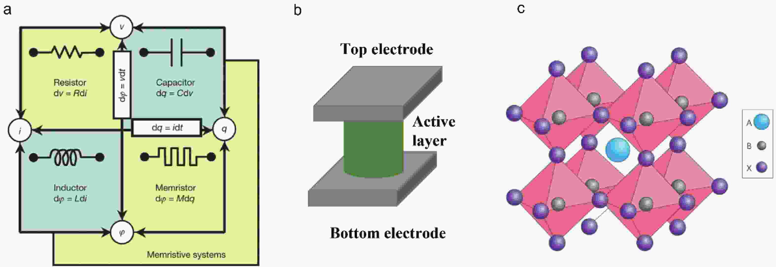
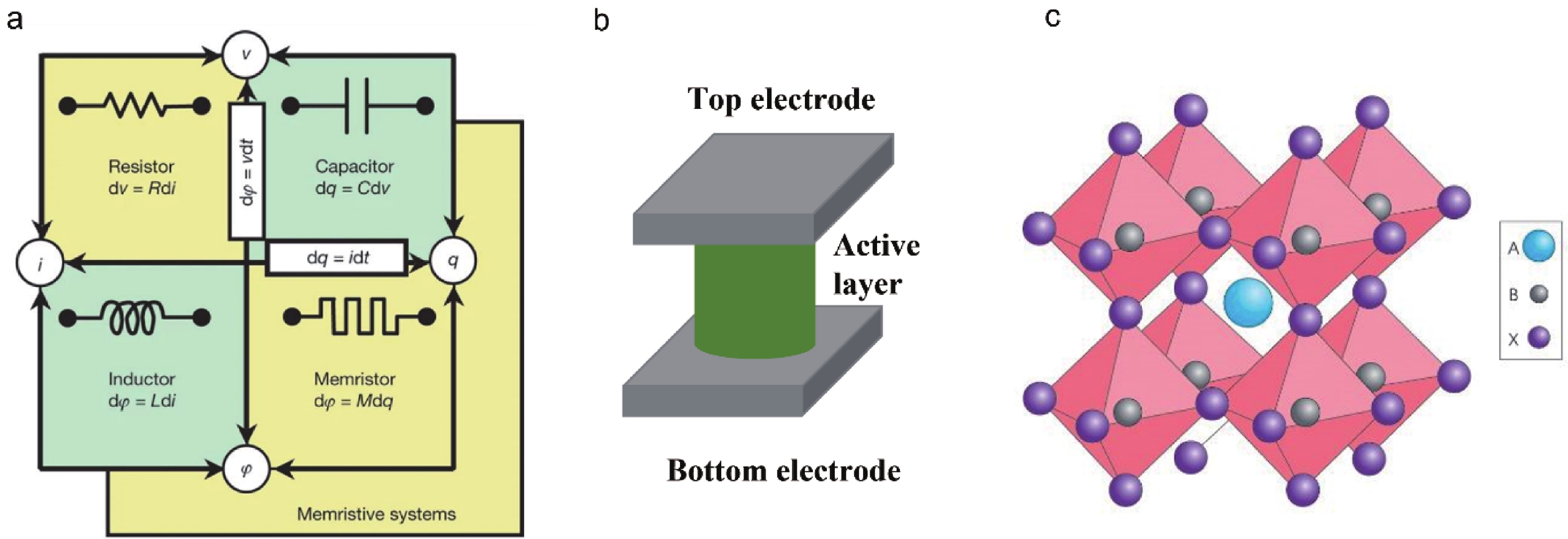
Fig. 1.  (Color online) (a) The basic four elements of an electrical circuit. Reproduced with permission from Ref. [3]. Copyright 2008, Nature publisher. (b) MIM structure of a memristor. (c) ABX3 structure of perovskite (A and B: cations and X: anion). Reproduced with permission from Ref. [18]. Copyright 2014, Nature publisher.

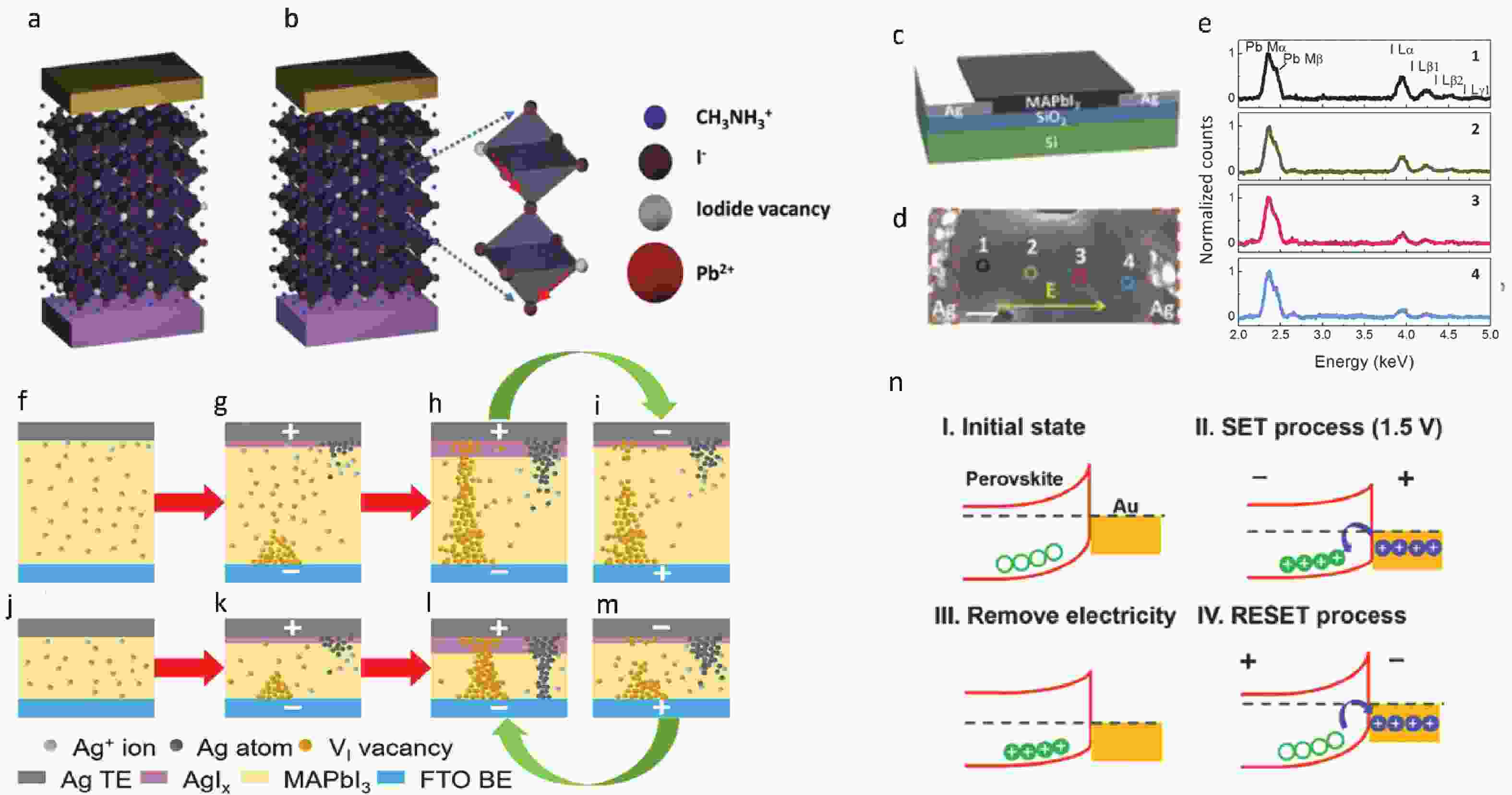
Fig. 2.  (Color online) Different switching mechanisms in OHP memristors. (a) Iodide vacancies are arbitrarily distributed. (b) Iodide vacancies aligned under influence of applied voltage. Inset: Movement of vacancies along the octahedral edge of structure. Reproduced with permission from Ref. [23]. Copyright 2016, American Chemical Society. (c) Architecture of Ag/MAPbI3/Ag device. (d) SEM micrograph showing 1−4 positions for EDS analysis. (e) EDS spectrum of device at LRS showing Pb and I peak intensities at four different positions shown in SEM image. Reproduced with permission from Ref. [24]. Copyright 2017, WILEY. Steps of RS via double-filament model in the Ag/MAPbI3/FTO memory device. (f) The initial state (HRS), (g) forming, (h) SET (LRS), and (i) RESET process of the device with thick MAPbI3 layer. (j) The initial state, (k) forming, (l) SET, and (m) RESET process of the device with relatively thinner MAPbI3. Reproduced with permission from Ref. [29]. Copyright 2016, American Chemical Society. (n) Mechanism of electrical switching (Ⅰ) initial state corresponding to HRS: hole trapping centres locate at the perovskite surface; (Ⅱ) SET process: Hole trap states are filled, shifting the Fermi level to the valence band; (Ⅲ) remove light electricity: a lowered barrier and quasi ohmic contact are resulted corresponding to LRS; and (Ⅳ) electrical reset: Holes are extracted from the trap states and a transition from LRS to HRS occurs. Reproduced with permission from Ref. [30]. Copyright 2018, WILEY.

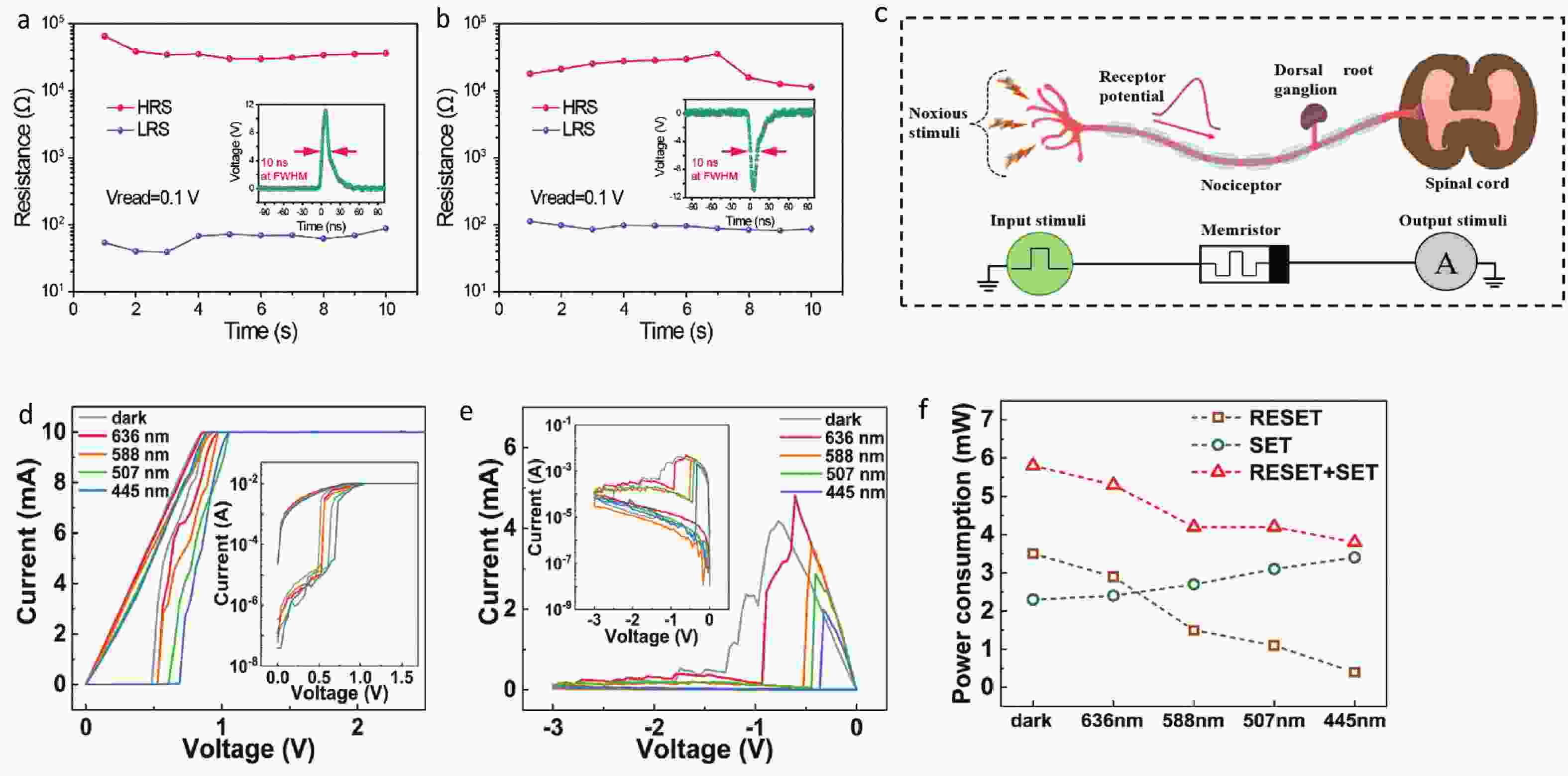
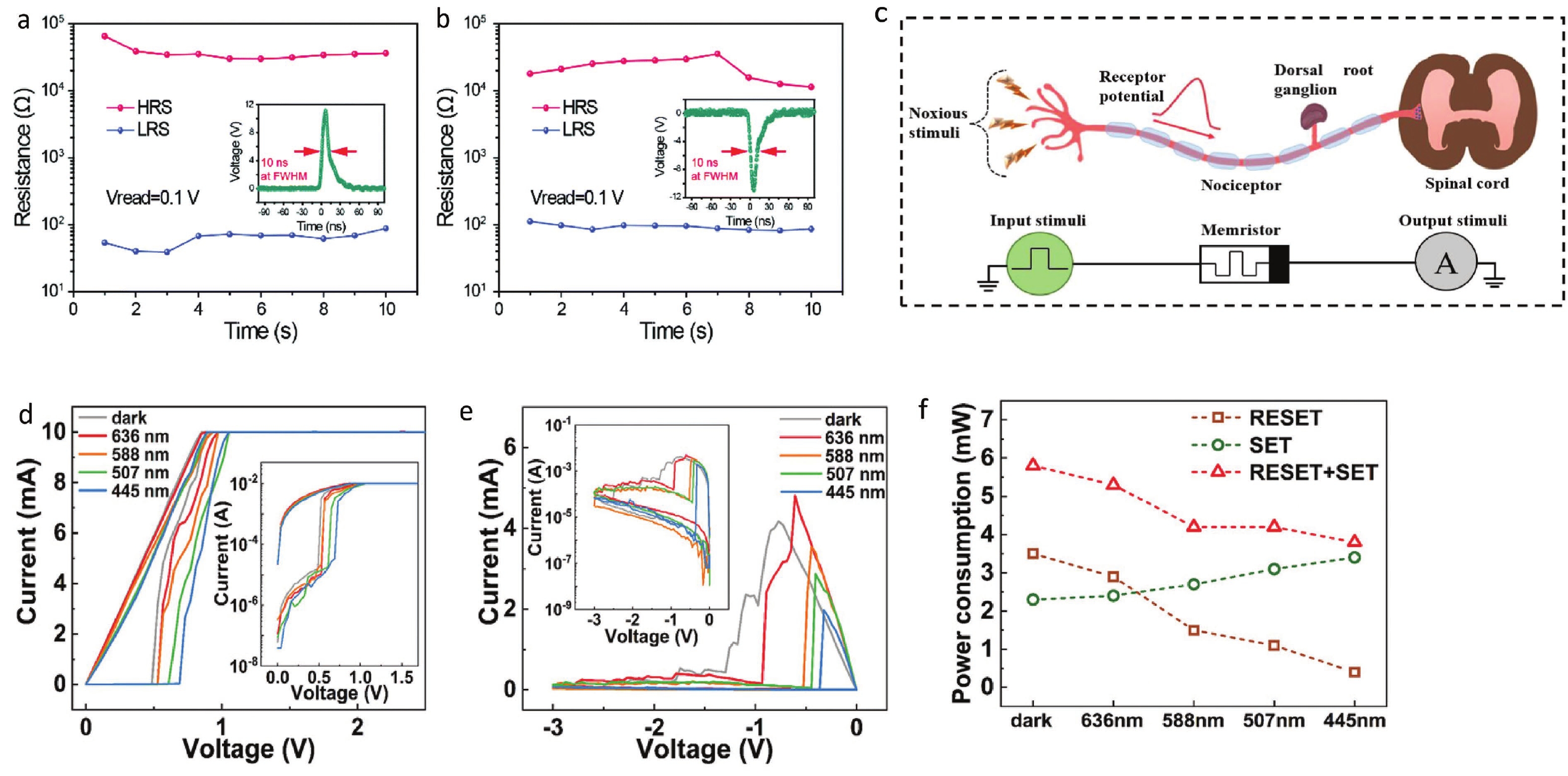
Fig. 3.  (Color online) High and low resistance states of MBI ReRAM under influence of 10 ns, (a) 10 V writing pulse, (b) -10 V erasing pulse. Insets show the incident writing and erasing voltage pulse. Reproduced with permission from Ref. [36]. Copyright 2021, Royal Society of Chemistry. (c) Schematic illustration of biological (top) and artificial (bottom) nociceptor. Reproduced with permission from Ref. [49]. Copyright 2023, American Chemical Society. RS trend in EGaIn/MAPbI3/PEDOT: PSS/ITO (d) SET process and (e) RESET process in dark and in presence of different wavelengths: 636, 588, 507, and 445 nm. Insets show the logarithmic scales of the same processes. (f) Power consumption for SET, RESET and total power consumption under the influence of different light signals. Reproduced with permission from Ref. [17]. Copyright 2023, WILEY.

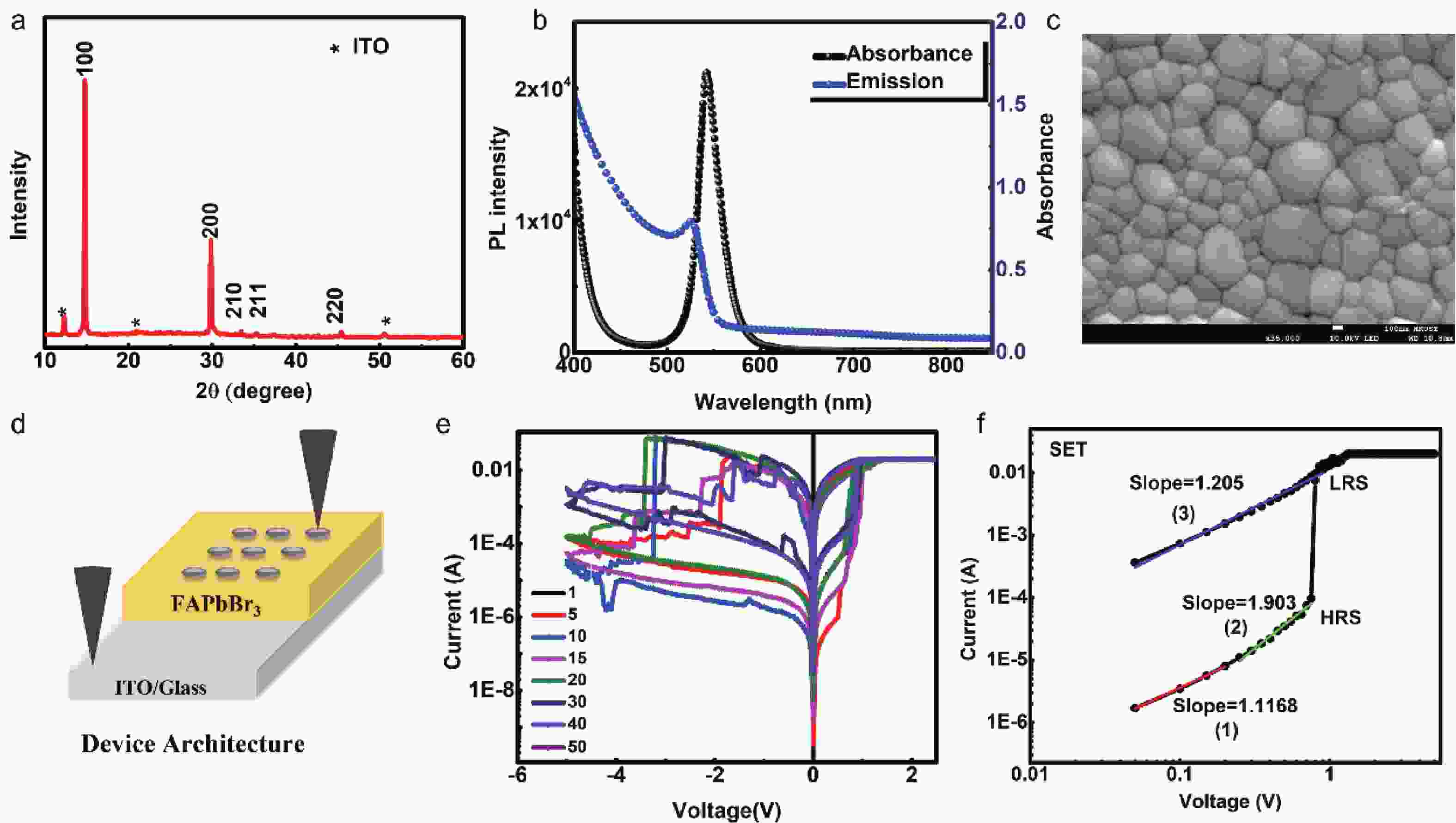
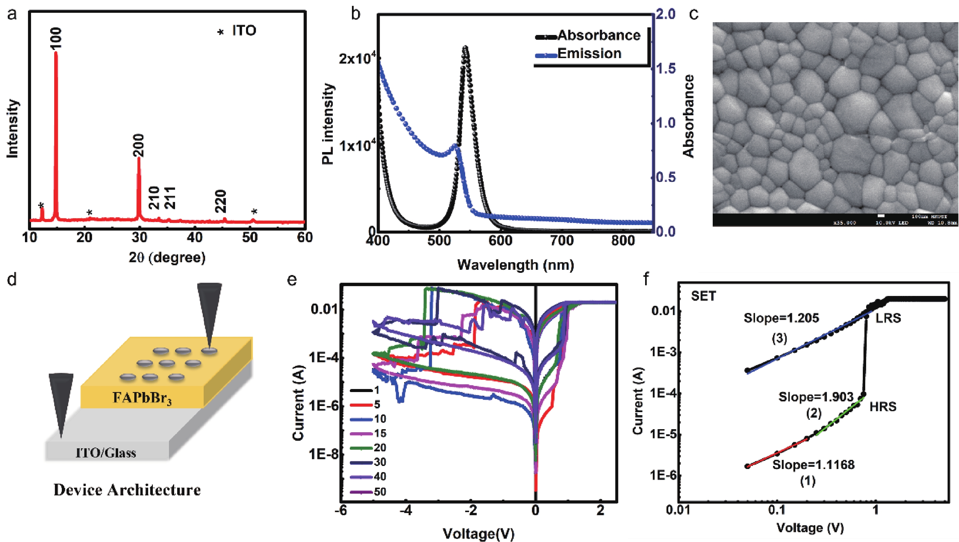
Fig. 4.  (Color online) Material characterization of FAPbBr3. (a) XRD, (b) UV-VIS and PL spectra, (c) SEM micrograph, (d) device design, (e) RS cycles for as fabricated device, and (f) conductive mechanism via measured and fitted curve for SET state.

Fig. 5.  (Color online) (a) Transmission spectra of pristine PMMA film and MAPbBr3 QDs with a complete device shown in inset. (b) RS cycles of MAPbBr3 QDs based memristor. Reproduced with permission from Ref. [42]. Copyright 2017, AIP Publishing. (c) Device architecture of MAPbI3 QWs/NWs on PET substrate with an enlarged view of QW sandwiched between Ag and Au and crystal structure of MAPbI3. Reproduced with permission from Ref. [50]. Copyright 2021, American Chemical Society.

Table 1.   Summary of device performances of some OHP based memristors.

StructureMethod of synthesisStructureON/OFF
ratio
Von (V)Voff (V)EnduranceRetention (s)MechanismRef
FTO/MAPbI3-xClx/AuSolution method3D40.8-0.6>103>4 × 10⁴Ag conductive filament[31]
PET/ITO/MAPbI3/Au3Antisolvent assisted spin coatAntisolvent assisted spin coating 3D500.7-0.5400104Defect migrationDefect migration[23]
FTO/c-TiO2/
MAPbI3-xClx/Al
Spin coating3D1.9 × 1091.10−1.65Active metal filament[26]
FTO/CH3NH3PbI3/WAntisolvent assisted spin coating3D>1003.1-1.1>100Schottky emission and ohmic conduction[32]
ITO/PEDOT: PSS/CH3NH3PbI3/
PCBM/Ag
Antisolvent assisted spin coating3D1.3 × 1030.13-0.23103Ion migration[33]
PET/ITO/MASnBr3/
Au
Antisolvent assisted spin coating3D1000.65 ± 0.15 V−3.1 
± 0.6 V
200104Formation and deformation of VBr[34]
ITO/PEDOT:PSS/
MAPbI3/Au
2 step spin coating3D200500[35]
ITO/MA3Bi2I9/CuChemical vapor deposition (CVD)3D1041−6.91.73 × 103>3 × 10⁵Active metal filament[36]
EGaIn/MAPbI3/
PEDOT: PSS/ITO
Antisolvent assisted spin coating3D4.3 × 1030.69−0.41104105VI migration[17]
Si/SiO2/Ti/Pt/
BA2MAn-1PbnI3n+1/Ag
Antisolvent assisted spin coating2D1070.4–1.2−1.2 to
−0.4
2501.08 × 104Ag or VI CF[37]
Graphene/
(PEA)2PbBr4/Au
Exfoliation2D10+7.6−1.0100103VBr CF[38]
ITO/BA2PbBr4/AuVapor deposition2D2.4 × 1033−36 0103VBr CF[39]
Si/SiO2/Ti/Pt/
(PEA)2Cs3Pb4I13/Ag
Spin coating2D1090.40−0.102302 × 10³Ag CF[40]
F40/MAPbBr1.97Cl1.03/AgSpin coatingNanoparticles5000.55−0.52501 × 10³Surface defects/grain boundaries generated due to Cl substitution[41]
PET/ITO/PMMA/41APbBr3 PeQDs: PMMA/PMMA/AgSpin coatingQuantum dots>1031−14 × 103Trap controlled SCLC[42]
42u/CH3NH3PbI3/PtVapour deposition>1031−1500>105[43]
DownLoad: CSV
[1]
Chua L. Memristor-The missing circuit element. IEEE Trans Circuit Theory, 1971, 18, 507 doi: 10.1109/TCT.1971.1083337
[2]
Hickmott T W. Low-frequency negative resistance in thin anodic oxide films. J Appl Phys, 1962, 33, 2669 doi: 10.1063/1.1702530
[3]
Strukov D B, Snider G S, Stewart D R, et al. The missing memristor found. Nature, 2008, 453, 80 doi: 10.1038/nature06932
[4]
Chua L. Resistance switching memories are memristors. Handbook of memristor networks, 2019, 197
[5]
Kim S, Du C, Sheridan P, et al. Experimental demonstration of a second-order memristor and its ability to biorealistically implement synaptic plasticity. Nano Lett, 2015, 15, 2203 doi: 10.1021/acs.nanolett.5b00697
[6]
Chen W B, Song L K, Wang S B, et al. Essential characteristics of memristors for neuromorphic computing. Adv Elect Materials, 2023, 9, 2200833 doi: 10.1002/aelm.202200833
[7]
Cryer M E, Fiedler H, Halpert J E. Photo-electrosensitive memristor using oxygen doping in HgTe nanocrystal films. ACS Appl Mater Interfaces, 2018, 10, 18927 doi: 10.1021/acsami.8b05429
[8]
Hu Z J, Cao F, Yan T T, et al. In situ vulcanization synthesis of CuInS2 nanosheet arrays for a memristor with a high on–off ratio and low power consumption. J Mater Chem C, 2023, 11, 244 doi: 10.1039/D2TC04003D
[9]
Aabel P, Sai Guru Srinivasan S, Amiruddin R, et al. Bi-polar switching properties of FTO/CZTS/Ag device. J Mater Sci Mater Electron, 2023, 34, 1 doi: 10.1007/s10854-022-09392-2
[10]
Li Y, Zhong Y P, Xu L, et al. Ultrafast synaptic events in a chalcogenide memristor. Sci Rep, 2013, 3, 1619 doi: 10.1038/srep01619
[11]
Hu H R, Scholz A, Liu Y, et al. A fully inkjet-printed unipolar metal oxide memristor for nonvolatile memory in printed electronics. IEEE Trans Electron Devices, 2023, 70, 3051 doi: 10.1109/TED.2023.3269405
[12]
Sato K, Hayashi Y, Masaoka N, et al. High-temperature operation of gallium oxide memristors up to 600 K. Sci Rep, 2023, 13, 1 doi: 10.1038/s41598-022-26890-9
[13]
Basnet P, Anderson E C, Athena F F, et al. Asymmetric resistive switching of bilayer HfO x /AlO y and AlO y /HfO x memristors: The oxide layer characteristics and performance optimization for digital set and analog reset switching. ACS Appl Electron Mater, 2023, 5, 1859 doi: 10.1021/acsaelm.3c00079
[14]
Prezioso M, Merrikh-Bayat F, Hoskins B D, et al. Training and operation of an integrated neuromorphic network based on metal-oxide memristors. Nature, 2015, 521, 61 doi: 10.1038/nature14441
[15]
Wu Y H, Huang H Y, Xu C, et al. The FAPbI3 perovskite memristor with a PMMA passivation layer as an artificial synapse. Appl Phys A, 2023, 129, 1 doi: 10.1007/s00339-022-06289-z
[16]
Guo Z C, Xiong R, Zhu Y Y, et al. High-performance and humidity robust multilevel lead-free all-inorganic Cs3Cu2Br5 perovskite-based memristors. Appl Phys Lett, 2023, 122, 053502. doi: 10.1063/5.0129311
[17]
Liu Z H, Cheng P P, Kang R Y, et al. Photo-enhanced resistive switching effect in high-performance MAPbI3 memristors. Adv Materials Inter, 2023, 10, 2201513 doi: 10.1002/admi.202201513
[18]
Green M A, Ho-Baillie A, Snaith H J. The emergence of perovskite solar cells. Nat Photonics, 2014, 8, 506 doi: 10.1038/nphoton.2014.134
[19]
Bati A S R, Zhong Y L, Burn P L, et al. Next-generation applications for integrated perovskite solar cells. Commun Mater, 2023, 4, 1 doi: 10.1038/s43246-022-00329-0
[20]
DeQuilettes D W, Zhang W, Burlakov V M, et al. Photo-induced halide redistribution in organic–inorganic perovskite films. Nat Commun, 2016, 7, 1 doi: 10.1038/ncomms11683
[21]
Xiao Z G, Yuan Y B, Shao Y C, et al. Giant switchable photovoltaic effect in organometal trihalide perovskite devices. Nat Mater, 2015, 14, 193 doi: 10.1038/nmat4150
[22]
Zhang C, Li Y, Ma C L, et al. Recent progress of organic–inorganic hybrid perovskites in RRAM, artificial synapse, and logic operation. Small Sci, 2022, 2, 2100086 doi: 10.1002/smsc.202100086
[23]
Gu C, Lee J S. Flexible hybrid organic–inorganic perovskite memory. ACS Nano, 2016, 10, 5413 doi: 10.1021/acsnano.6b01643
[24]
Zhu X J, Lee J H, Lu W D. Perovskite films: Iodine vacancy redistribution in organic-inorganic halide perovskite films and resistive switching effects. Adv Mater, 2017, 29, 1700527 doi: 10.1002/adma.201700527
[25]
Kim D J, Tak Y J, Kim W G, et al. Resistive switching properties through iodine migrations of a hybrid perovskite insulating layer. Adv Mater Interfaces, 2017, 4, 1601035 doi: 10.1002/admi.201601035
[26]
Yan K, Peng M, Yu X, et al. High-performance perovskite memristor based on methyl ammonium lead halides. J Mater Chem C, 2016, 4, 1375 doi: 10.1039/C6TC00141F
[27]
Yoo E, Lyu M Q, Yun J H, et al. Bifunctional resistive switching behavior in an organolead halide perovskite based Ag/CH3NH3PbI3− x Cl x /FTO structure. J Mater Chem C, 2016, 4, 7824 doi: 10.1039/C6TC02503J
[28]
Wang W, Xu J Q, Ma H L, et al. Insertion of nanoscale AgInSbTe layer between the Ag electrode and the CH3NH3PbI3 electrolyte layer enabling enhanced multilevel memory. ACS Appl Nano Mater, 2019, 2, 307 doi: 10.1021/acsanm.8b01928
[29]
Sun Y M, Tai M Q, Song C, et al. Competition between metallic and vacancy defect conductive filaments in a CH3NH3PbI3-based memory device. J Phys Chem C, 2018, 122, 6431 doi: 10.1021/acs.jpcc.7b12817
[30]
Zhou F C, Liu Y H, Shen X P, et al. Low-voltage, optoelectronic CH3NH3PbI3– x Cl x memory with integrated sensing and logic operations. Adv Funct Mater, 2018, 28, 1800080 doi: 10.1002/adfm.201800080
[31]
Yoo E J, Lyu M Q, Yun J H, et al. Resistive switching behavior in organic-inorganic hybrid CH3NH3PbI3 –x Cl x Perovskite for resistive random access memory devices. Adv Mater, 2015, 27, 6170 doi: 10.1002/adma.201502889
[32]
Cai H M, Ma G K, He Y L, et al. A remarkable performance of CH3NH3PbI3 perovskite memory based on passivated method. Org Electron, 2018, 58, 301 doi: 10.1016/j.orgel.2018.04.025
[33]
Gogoi H J, Mallajosyula A T. Enhancing the switching performance of CH3NH3PbI3 memristors by the control of size and characterization parameters. Adv Elect Materials, 2021, 7, 2100472 doi: 10.1002/aelm.202100472
[34]
Qian W H, Cheng X F, Zhou J, et al. Lead-free perovskite MASnBr3-based memristor for quaternary information storage. InfoMat, 2020, 2, 743 doi: 10.1002/inf2.12066
[35]
Xiao Z G, Huang J S. Energy-efficient hybrid perovskite memristors and synaptic devices. Adv Electron Mater, 2016, 2, 1600100 doi: 10.1002/aelm.201600100
[36]
Poddar S, Zhang Y T, Zhu Y Y, et al. Optically tunable ultra-fast resistive switching in lead-free methyl-ammonium bismuth iodide perovskite films. Nanoscale, 2021, 13, 6184 doi: 10.1039/D0NR09234G
[37]
Seo J Y, Choi J, Kim H S, et al. Wafer-scale reliable switching memory based on 2-dimensional layered organic–inorganic halide perovskite. Nanoscale, 2017, 9, 15278 doi: 10.1039/C7NR05582J
[38]
Tian H, Zhao L F, Wang X F, et al. Extremely low operating current resistive memory based on exfoliated 2D perovskite single crystals for neuromorphic computing. ACS Nano, 2017, 11, 12247 doi: 10.1021/acsnano.7b05726
[39]
Lee D, Hwang B, Lee J S. Impact of grain sizes on programmable memory characteristics in two-dimensional organic–inorganic hybrid perovskite memory. ACS Appl Mater Interfaces, 2019, 11, 20225 doi: 10.1021/acsami.9b05038
[40]
Kim H, Choi M J, Suh J M, et al. Quasi-2D halide perovskites for resistive switching devices with ON/OFF ratios above 109. NPG Asia Mater, 2020, 12, 21 doi: 10.1038/s41427-019-0187-x
[41]
Muthu C, Agarwal S, Vijayan A, et al. Hybrid perovskite nanoparticles for high-performance resistive random access memory devices: Control of operational parameters through chloride doping. Adv Mater Interfaces, 2016, 3, 1600092 doi: 10.1002/admi.201600092
[42]
Yang K Y, Li F S, Veeramalai C P, et al. A facile synthesis of CH3NH3PbBr3 perovskite quantum dots and their application in flexible nonvolatile memory. Appl Phys Lett, 2017, 110, 083102 doi: 10.1063/1.4976709
[43]
Hwang B, Lee J S. A strategy to design high-density nanoscale devices utilizing vapor deposition of metal halide perovskite materials. Adv Mater, 2017, 29, 1701048 doi: 10.1002/adma.201701048
[44]
Hwang B, Gu C, Lee D, et al. Effect of halide-mixing on the switching behaviors of organic-inorganic hybrid perovskite memory. Sci Rep, 2017, 7, 43794 doi: 10.1038/s41598-016-0028-x
[45]
Zhang X H, Zhao X N, Shan X Y, et al. Humidity effect on resistive switching characteristics of the CH3NH3PbI3 memristor. ACS Appl Mater Interfaces, 2021, 13, 28555 doi: 10.1021/acsami.1c05590
[46]
Cheng X F, Qian W H, Wang J, et al. Environmentally robust memristor enabled by lead-free double perovskite for high-performance information storage. Small, 2019, 15, 1905731 doi: 10.1002/smll.201905731
[47]
John R A, Yantara N, Ng Y F, et al. Ionotronic halide perovskite drift-diffusive synapses for low-power neuromorphic computation. Adv Mater, 2018, 30, 1805454 doi: 10.1002/adma.201805454
[48]
Shivarudraiah S B, Tewari N, Ng M, et al. Optically clear films of formamidinium lead bromide perovskite for wide-band-gap, solution-processed, semitransparent solar cells. ACS Appl Mater Interfaces, 2021, 13, 37223 doi: 10.1021/acsami.1c10657
[49]
Patil H, Kim H, Kadam K D, et al. Flexible organic–inorganic halide perovskite-based diffusive memristor for artificial nociceptors. ACS Appl Mater Interfaces, 2023, 15, 13238 doi: 10.1021/acsami.2c16481
[50]
Poddar S, Zhang Y T, Gu L L, et al. Down-scalable and ultra-fast memristors with ultra-high density three-dimensional arrays of perovskite quantum wires. Nano Lett, 2021, 21, 5036 doi: 10.1021/acs.nanolett.1c00834
[51]
Guan X W, Wan T, Hu L, et al. A solution-processed all-perovskite memory with dual-band light response and tri-mode operation. Adv Funct Materials, 2022, 32, 2110975 doi: 10.1002/adfm.202110975
[52]
Kulbak M, Gupta S, Kedem N, et al. Cesium enhances long-term stability of lead bromide perovskite-based solar cells. J Phys Chem Lett, 2016, 7, 167 doi: 10.1021/acs.jpclett.5b02597
[53]
Le Q V, Lee J W, Sohn W, et al. Low temperature solution-processable cesium lead bromide microcrystals for light conversion. Cryst Growth Des, 2018, 18, 3161 doi: 10.1021/acs.cgd.8b00264
[54]
Guan X W, Lei Z H, Yu X C, et al. Low-dimensional metal-halide perovskites as high-performance materials for memory applications. Small, 2022, 18, 2203311 doi: 10.1002/smll.202203311
[55]
Hu L, Zhao Q, Huang S J, et al. Flexible and efficient perovskite quantum dot solar cells via hybrid interfacial architecture. Nat Commun, 2021, 12, 466 doi: 10.1038/s41467-020-20314-w
[56]
Yin J, Maity P, Naphade R, et al. Tuning hot carrier cooling dynamics by dielectric confinement in two-dimensional hybrid perovskite crystals. ACS Nano, 2019, 13, 12621 doi: 10.1021/acsnano.9b04085
[57]
Kim J, Hu L, Chen H J, et al. P-type charge transport and selective gas sensing of all-inorganic perovskite nanocrystals. ACS Mater Lett, 2020, 2, 1368 doi: 10.1021/acsmaterialslett.0c00346
[58]
Cheng X F, Hou X, Zhou J, et al. Pseudohalide-induced 2D (CH3NH3)2PbI2(SCN)2 perovskite for ternary resistive memory with high performance. Small, 2018, 14, 1703667 doi: 10.1002/smll.201703667
[59]
Zhao J, Li S J, Tong W C, et al. Light-induced anomalous resistive switches based on individual organic-inorganic halide perovskite micro-/ nanofibers. Adv Electron Mater, 2018, 4, 1800206 doi: 10.1002/aelm.201800206
[60]
Jiang T H, Shao Z B, Fang H, et al. High-performance nanofloating gate memory based on lead halide perovskite nanocrystals. ACS Appl Mater Interfaces, 2019, 11, 24367 doi: 10.1021/acsami.9b03474
[61]
Yang J Q, Wang R P, Wang Z P, et al. Leaky integrate-and-fire neurons based on perovskite memristor for spiking neural networks. Nano Energy, 2020, 74, 104828 doi: 10.1016/j.nanoen.2020.104828
[62]
Zhang Y T, Poddar S, Huang H, et al. Three-dimensional perovskite nanowire array–based ultrafast resistive RAM with ultralong data retention. Sci Adv, 2021, 7, eabg3788 doi: 10.1126/sciadv.abg3788
  • Search

    Advanced Search >>

    GET CITATION

    shu

    Export: BibTex EndNote

    Article Metrics

    Article views: 663 Times PDF downloads: 72 Times Cited by: 0 Times

    History

    Received: 20 June 2023 Revised: 18 August 2023 Online: Accepted Manuscript: 13 September 2023Corrected proof: 14 September 2023Uncorrected proof: 15 September 2023Published: 10 September 2023

    Catalog

      Email This Article

      User name:
      Email:*请输入正确邮箱
      Code:*验证码错误
      Memoona Qammar, Bosen Zou, Jonathan E. Halpert. Organic-inorganic halide perovskites for memristors[J]. Journal of Semiconductors, 2023, 44(9): 091604. doi: 10.1088/1674-4926/44/9/091604 M Qammar, B Zou, J E. Halpert. Organic-inorganic halide perovskites for memristors[J]. J. Semicond, 2023, 44(9): 091604. doi: 10.1088/1674-4926/44/9/091604Export: BibTex EndNote
      Citation:
      Memoona Qammar, Bosen Zou, Jonathan E. Halpert. Organic-inorganic halide perovskites for memristors[J]. Journal of Semiconductors, 2023, 44(9): 091604. doi: 10.1088/1674-4926/44/9/091604

      M Qammar, B Zou, J E. Halpert. Organic-inorganic halide perovskites for memristors[J]. J. Semicond, 2023, 44(9): 091604. doi: 10.1088/1674-4926/44/9/091604
      Export: BibTex EndNote

      Organic-inorganic halide perovskites for memristors

      doi: 10.1088/1674-4926/44/9/091604
      More Information
      • Author Bio:

        Memoona Qammar got her bachelor’s degree in chemistry from University of Sargodha Pakistan in 2014 and master’s degree from National University of Sciences and Technology (NUST) Pakistan in 2017. Now she is a doctoral student at The Hong Kong University of Science and Technology (HKUST) Hong Kong under supervision of Prof. Jonathan Halpert. Currently, her work focusses on the optoelectronic properties of perovskites

        Jonathan E. Halpert received his PhD from the Massachusetts Institute of Technology (MIT) in 2008. He is currently an assistant professor in the Department of Chemistry at The Hong Kong University of Science & Technology (HKUST). His work is currently focused on optoelectronic devices made from perovskite and copper halide nanocrystals

      • Corresponding author: jhalpert@ust.hk
      • Received Date: 2023-06-20
      • Revised Date: 2023-08-18
      • Available Online: 2023-09-13

      Catalog

        /

        DownLoad:  Full-Size Img  PowerPoint
        Return
        Return