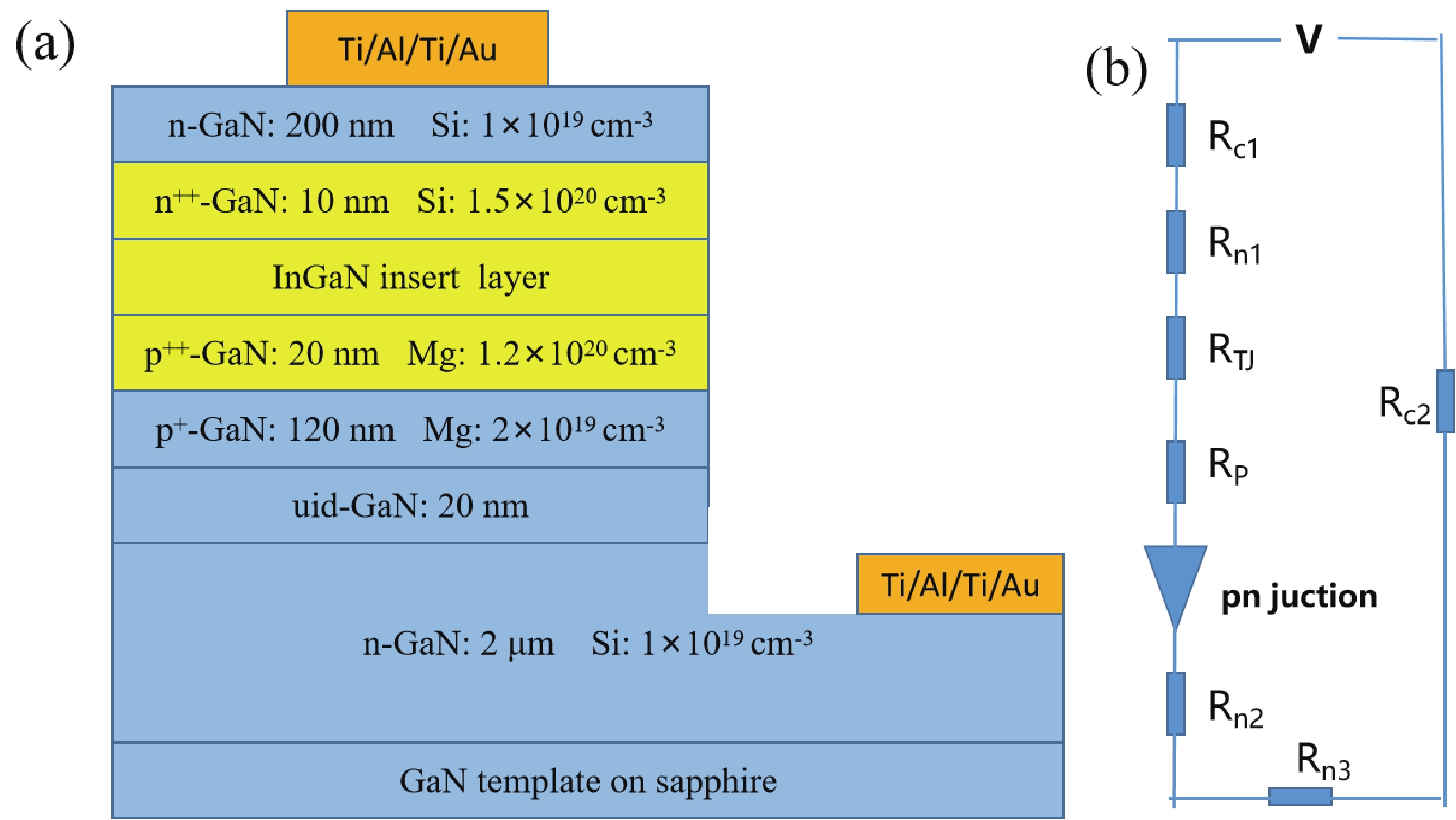
Fig. 1.
(Color online) (a) Schematic diagram of the device structure including GaN/InGaN/GaN TJ. (b) Equivalent circuit diagram of the device.
ARTICLES
Jun Fang1, 2, Fan Zhang2, Wenxian Yang2, , Aiqin Tian2, Jianping Liu2, Shulong Lu2 and Hui Yang2,
Corresponding author: Wenxian Yang, wxyang2014@sinano.ac.cn; Hui Yang, hyang2006@sinano.ac.cn
Abstract: The InGaN films and GaN/InGaN/GaN tunnel junctions (TJs) were grown on GaN templates with plasma-assisted molecular beam epitaxy. As the In content increases, the quality of InGaN films grown on GaN templates decreases and the surface roughness of the samples increases. V-pits and trench defects were not found in the AFM images. p++-GaN/InGaN/n++-GaN TJs were investigated for various In content, InGaN thicknesses and doping concentration in the InGaN insert layer. The InGaN insert layer can promote good interband tunneling in GaN/InGaN/GaN TJ and significantly reduce operating voltage when doping is sufficiently high. The current density increases with increasing In content for the 3 nm InGaN insert layer, which is achieved by reducing the depletion zone width and the height of the potential barrier. At a forward current density of 500 A/cm2, the measured voltage was 4.31 V and the differential resistance was measured to be 3.75 × 10⁻³ Ω·cm2 for the device with a 3 nm p++-In0.35Ga0.65N insert layer. When the thickness of the In0.35Ga0.65N layer is closer to the “balanced” thickness, the TJ current density is higher. If the thickness is too high or too low, the width of the depletion zone will increase and the current density will decrease. The undoped InGaN layer has a better performance than n-type doping in the TJ. Polarization-engineered tunnel junctions can enhance the functionality and performance of electronic and optoelectronic devices.
Key words: GaN/InGaN/GaN, tunnel junctions, polarization-engineering, molecular beam epitaxy
| [1] |
Takeuchi T, Hasnain G, Corzine S, et al. GaN-based light emitting diodes with tunnel junctions. Jpn J Appl Phys, 2001, 40, L861 doi: 10.1143/JJAP.40.L861
|
| [2] |
Ozden I, Makarona E, Nurmikko A V, et al. A dual-wavelength indium gallium nitride quantum well light emitting diode. Appl Phys Lett, 2001, 79, 2532 doi: 10.1063/1.1410345
|
| [3] |
Song Y K, Zhou H, Diagne M, et al. A vertical cavity light emitting InGaN quantum well heterostructure. Appl Phys Lett, 1999, 74, 3441 doi: 10.1063/1.124121
|
| [4] |
Jeon S R, Oh C S, Yang J W, et al. GaN tunnel junction as a current aperture in a blue surface-emitting light-emitting diode. Appl Phys Lett, 2002, 80, 1933 doi: 10.1063/1.1459487
|
| [5] |
Diagne M, He Y, Zhou H, et al. Vertical cavity violet light emitting diode incorporating an aluminum gallium nitride distributed Bragg mirror and a tunnel junction. Appl Phys Lett, 2001, 79, 3720 doi: 10.1063/1.1415405
|
| [6] |
Krishnamoorthy S, Akyol F, Rajan S. InGaN/GaN tunnel junctions for hole injection in GaN light emitting diodes. Appl Phys Lett, 2014, 105, 141104 doi: 10.1063/1.4897342
|
| [7] |
Krishnamoorthy S, Nath D N, Akyol F, et al. Polarization-engineered GaN/InGaN/GaN tunnel diodes. Appl Phys Lett, 2010, 97, 203502 doi: 10.1063/1.3517481
|
| [8] |
Zhang Z H, Tiam Tan S, Kyaw Z, et al. InGaN/GaN light-emitting diode with a polarization tunnel junction. Appl Phys Lett, 2013, 102, 193508 doi: 10.1063/1.4806978
|
| [9] |
Young E C, Yonkee B P, Wu F, et al. Hybrid tunnel junction contacts to III–nitride light-emitting diodes. Appl Phys Express, 2016, 9, 022102 doi: 10.7567/APEX.9.022102
|
| [10] |
Kaga M, Morita T, Kuwano Y, et al. GaInN-based tunnel junctions in n–p–n light emitting diodes. Jpn J Appl Phys, 2013, 52, 08JH06 doi: 10.7567/JJAP.52.08JH06
|
| [11] |
Yang J, Zhao D G, Liu Z S, et al. A 357.9 nm GaN/AlGaN multiple quantum well ultraviolet laser diode. J Semicond, 2022, 43, 010501 doi: 10.1088/1674-4926/43/1/010501
|
| [12] |
Heikman S, Keller S, Wu Y, et al. Polarization effects in AlGaN/GaN and GaN/AlGaN/GaN heterostructures. J Appl Phys, 2003, 93, 10114 doi: 10.1063/1.1577222
|
| [13] |
Zhang M L, Ikeda M, Huang S Y, et al. Ni/Pd-based ohmic contacts to p-GaN through p-InGaN/p+-GaN contacting layers. J Semicond, 2022, 43, 092803 doi: 10.1088/1674-4926/43/9/092803
|
| [14] |
Li W J, Sharmin S, Ilatikhameneh H, et al. Polarization-engineered III-nitride heterojunction tunnel field-effect transistors. IEEE J Explor Solid State Comput Devices Circuits, 2015, 1, 28 doi: 10.1109/JXCDC.2015.2426433
|
| [15] |
Krishnamoorthy S, Park P S, Rajan S. Demonstration of forward inter-band tunneling in GaN by polarization engineering. Appl Phys Lett, 2011, 99, 233504 doi: 10.1063/1.3666862
|
| [16] |
Simon J, Zhang Z, Goodman K, et al. Polarization-induced zener tunnel junctions in wide-band-gap heterostructures. Phys Rev Lett, 2009, 103, 026801 doi: 10.1103/PhysRevLett.103.026801
|
| [17] |
Yan X D, Li W J, Islam S M, et al. Polarization-induced zener tunnel diodes in GaN/InGaN/GaN heterojunctions. Appl Phys Lett, 2015, 107, 163504 doi: 10.1063/1.4934269
|
| [18] |
Kuwano Y, Kaga M, Morita T, et al. Lateral hydrogen diffusion at p-GaN layers in nitride-based light emitting diodes with tunnel junctions. Jpn J Appl Phys, 2013, 52, 08JK12 doi: 10.7567/JJAP.52.08JK12
|
| [19] |
Akyol F, Zhang Y W, Krishnamoorthy S, et al. Ultralow-voltage-drop GaN/InGaN/GaN tunnel junctions with 12% indium content. Appl Phys Express, 2017, 10, 121003 doi: 10.7567/APEX.10.121003
|
| [20] |
Takasuka D, Akatsuka Y, Ino M, et al. GaInN-based tunnel junctions with graded layers. Appl Phys Express, 2016, 9, 081005 doi: 10.7567/APEX.9.081005
|
| [21] |
Pankove J I, Magee C W, Wance R O. Hole-mediated chemisorption of atomic hydrogen in silicon. Appl Phys Lett, 1985, 47, 748 doi: 10.1063/1.96026
|
| [22] |
Neugebauer J, Van de Walle C G. Role of hydrogen in doping of GaN. Appl Phys Lett, 1996, 68, 1829 doi: 10.1063/1.116027
|
| [23] |
Jiang L R, Liu J P, Tian A Q, et al. GaN-based green laser diodes. J Semicond, 2016, 37, 111001 doi: 10.1088/1674-4926/37/11/111001
|
| [24] |
Liang F, Zhao D G, Liu Z S, et al. GaN-based blue laser diode with 6.0 W of output power under continuous-wave operation at room temperature. J Semicond, 2021, 42, 112801 doi: 10.1088/1674-4926/42/11/112801
|
| [25] |
Pristovsek M, Kadir A, Meissner C, et al. Growth mode transition and relaxation of thin InGaN layers on GaN (0001). J Cryst Growth, 2013, 372, 65 doi: 10.1016/j.jcrysgro.2013.03.012
|
| [26] |
Suihkonen S, Svensk O, Lang T, et al. The effect of InGaN/GaN MQW hydrogen treatment and threading dislocation optimization on GaN LED efficiency. J Cryst Growth, 2007, 298, 740 doi: 10.1016/j.jcrysgro.2006.10.131
|
| [27] |
Massabuau F C P, Trinh-Xuan L, Lodié D, et al. Correlations between the morphology and emission properties of trench defects in InGaN/GaN quantum wells. J Appl Phys, 2013, 113, 073505 doi: 10.1063/1.4792505
|
| [28] |
Krishnamoorthy S, Akyol F, Park P S, et al. Low resistance GaN/InGaN/GaN tunnel junctions. Appl Phys Lett, 2013, 102, 113503 doi: 10.1063/1.4796041
|
| [29] |
Hamdy S W, Young E C, Alhassan A I, et al. Efficient tunnel junction contacts for high-power semipolar III-nitride edge-emitting laser diodes. Opt Express, 2019, 27, 8327 doi: 10.1364/OE.27.008327
|
| [30] |
Akatsuka Y, Iwayama S, Takeuchi T, et al. Doping profiles in low resistive GaN tunnel junctions grown by metalorganic vapor phase epitaxy. Appl Phys Express, 2019, 12, 025502 doi: 10.7567/1882-0786/aafca8
|
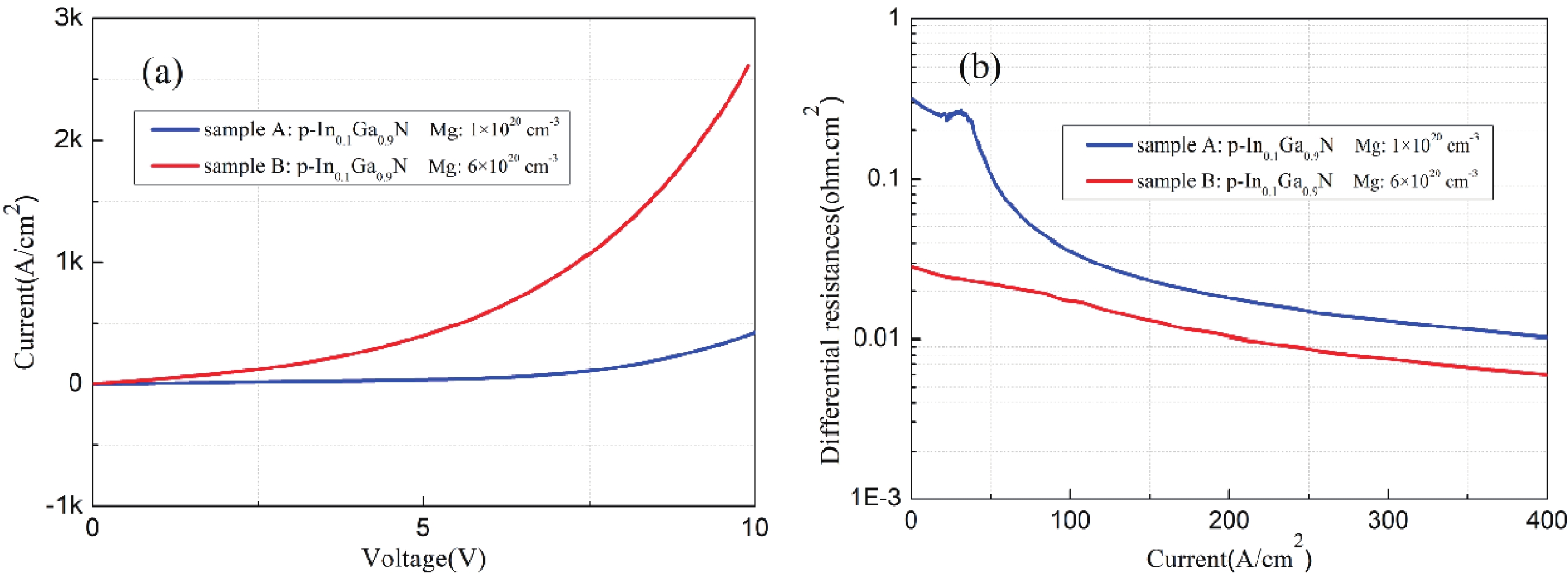
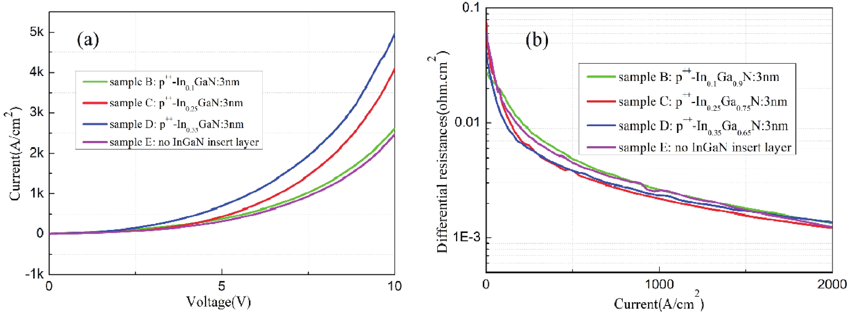
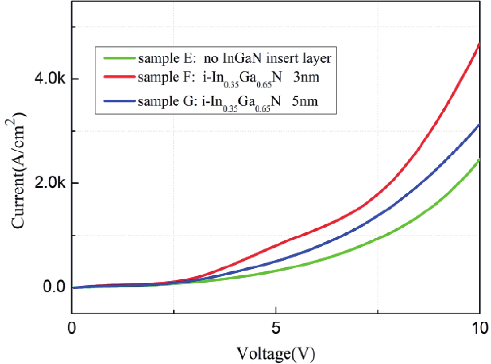
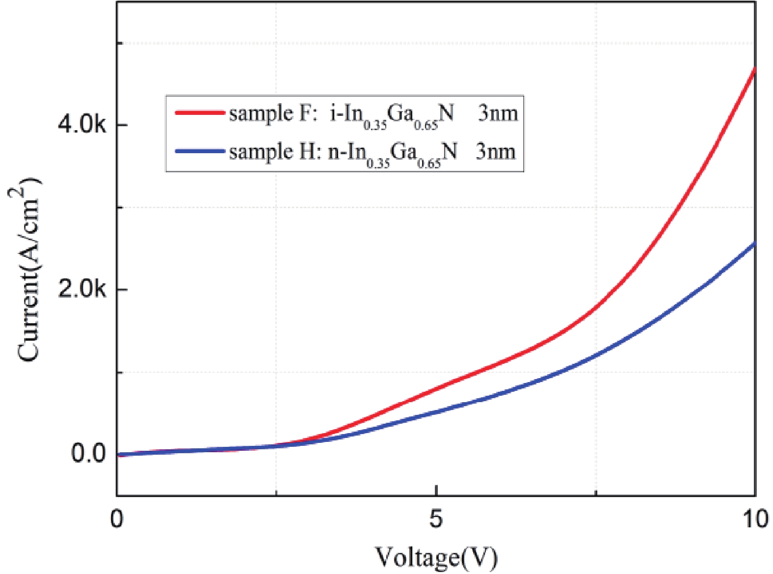
Table 1. The specific structural parameters of GaN/InGaN/GaN TJ.
| p++-GaN: 20 nm (1020 cm−3) | Insert layer InGaN | n++-GaN: 10 nm (1020 cm−3) | |
| Sample A |
Mg: 1 | p++-In0.1Ga0.9N: 3 nm Mg: 1 × 1020 cm−3 |
Si: 0.5 |
| Sample B |
Mg: 1.2 | p++-In0.1Ga0.9N: 3 nm Mg: 6 × 1020 cm−3 |
Si: 1.5 |
| Sample C | Mg: 1.2 |
p++-In0.25Ga0.75N: 3 nm Mg: 6 × 1020 cm−3 |
Si: 1.5 |
| Sample D | Mg: 1.2 | p++-In0.35Ga0.65N: 3 nm Mg: 6 × 1020 cm−3 |
Si: 1.5 |
| Sample E | Mg: 1.2 | No InGaN insert layer Mg: 6 × 1020 cm−3 |
Si: 1.5 |
| Sample F | Mg: 1.2 |
Uid-In0.35Ga0.65N: 3 nm | Si: 1.5 |
| Sample G | Mg: 1.2 |
Uid-In0.35Ga0.65N: 5 nm | Si: 1.5 |
| Sample H | Mg: 1.2 |
n-In0.35Ga0.65N: 3 nm Si: 2 × 1019 cm−3 |
Si: 1.5 |
 DownLoad: CSV
| [1] |
Takeuchi T, Hasnain G, Corzine S, et al. GaN-based light emitting diodes with tunnel junctions. Jpn J Appl Phys, 2001, 40, L861 doi: 10.1143/JJAP.40.L861
|
| [2] |
Ozden I, Makarona E, Nurmikko A V, et al. A dual-wavelength indium gallium nitride quantum well light emitting diode. Appl Phys Lett, 2001, 79, 2532 doi: 10.1063/1.1410345
|
| [3] |
Song Y K, Zhou H, Diagne M, et al. A vertical cavity light emitting InGaN quantum well heterostructure. Appl Phys Lett, 1999, 74, 3441 doi: 10.1063/1.124121
|
| [4] |
Jeon S R, Oh C S, Yang J W, et al. GaN tunnel junction as a current aperture in a blue surface-emitting light-emitting diode. Appl Phys Lett, 2002, 80, 1933 doi: 10.1063/1.1459487
|
| [5] |
Diagne M, He Y, Zhou H, et al. Vertical cavity violet light emitting diode incorporating an aluminum gallium nitride distributed Bragg mirror and a tunnel junction. Appl Phys Lett, 2001, 79, 3720 doi: 10.1063/1.1415405
|
| [6] |
Krishnamoorthy S, Akyol F, Rajan S. InGaN/GaN tunnel junctions for hole injection in GaN light emitting diodes. Appl Phys Lett, 2014, 105, 141104 doi: 10.1063/1.4897342
|
| [7] |
Krishnamoorthy S, Nath D N, Akyol F, et al. Polarization-engineered GaN/InGaN/GaN tunnel diodes. Appl Phys Lett, 2010, 97, 203502 doi: 10.1063/1.3517481
|
| [8] |
Zhang Z H, Tiam Tan S, Kyaw Z, et al. InGaN/GaN light-emitting diode with a polarization tunnel junction. Appl Phys Lett, 2013, 102, 193508 doi: 10.1063/1.4806978
|
| [9] |
Young E C, Yonkee B P, Wu F, et al. Hybrid tunnel junction contacts to III–nitride light-emitting diodes. Appl Phys Express, 2016, 9, 022102 doi: 10.7567/APEX.9.022102
|
| [10] |
Kaga M, Morita T, Kuwano Y, et al. GaInN-based tunnel junctions in n–p–n light emitting diodes. Jpn J Appl Phys, 2013, 52, 08JH06 doi: 10.7567/JJAP.52.08JH06
|
| [11] |
Yang J, Zhao D G, Liu Z S, et al. A 357.9 nm GaN/AlGaN multiple quantum well ultraviolet laser diode. J Semicond, 2022, 43, 010501 doi: 10.1088/1674-4926/43/1/010501
|
| [12] |
Heikman S, Keller S, Wu Y, et al. Polarization effects in AlGaN/GaN and GaN/AlGaN/GaN heterostructures. J Appl Phys, 2003, 93, 10114 doi: 10.1063/1.1577222
|
| [13] |
Zhang M L, Ikeda M, Huang S Y, et al. Ni/Pd-based ohmic contacts to p-GaN through p-InGaN/p+-GaN contacting layers. J Semicond, 2022, 43, 092803 doi: 10.1088/1674-4926/43/9/092803
|
| [14] |
Li W J, Sharmin S, Ilatikhameneh H, et al. Polarization-engineered III-nitride heterojunction tunnel field-effect transistors. IEEE J Explor Solid State Comput Devices Circuits, 2015, 1, 28 doi: 10.1109/JXCDC.2015.2426433
|
| [15] |
Krishnamoorthy S, Park P S, Rajan S. Demonstration of forward inter-band tunneling in GaN by polarization engineering. Appl Phys Lett, 2011, 99, 233504 doi: 10.1063/1.3666862
|
| [16] |
Simon J, Zhang Z, Goodman K, et al. Polarization-induced zener tunnel junctions in wide-band-gap heterostructures. Phys Rev Lett, 2009, 103, 026801 doi: 10.1103/PhysRevLett.103.026801
|
| [17] |
Yan X D, Li W J, Islam S M, et al. Polarization-induced zener tunnel diodes in GaN/InGaN/GaN heterojunctions. Appl Phys Lett, 2015, 107, 163504 doi: 10.1063/1.4934269
|
| [18] |
Kuwano Y, Kaga M, Morita T, et al. Lateral hydrogen diffusion at p-GaN layers in nitride-based light emitting diodes with tunnel junctions. Jpn J Appl Phys, 2013, 52, 08JK12 doi: 10.7567/JJAP.52.08JK12
|
| [19] |
Akyol F, Zhang Y W, Krishnamoorthy S, et al. Ultralow-voltage-drop GaN/InGaN/GaN tunnel junctions with 12% indium content. Appl Phys Express, 2017, 10, 121003 doi: 10.7567/APEX.10.121003
|
| [20] |
Takasuka D, Akatsuka Y, Ino M, et al. GaInN-based tunnel junctions with graded layers. Appl Phys Express, 2016, 9, 081005 doi: 10.7567/APEX.9.081005
|
| [21] |
Pankove J I, Magee C W, Wance R O. Hole-mediated chemisorption of atomic hydrogen in silicon. Appl Phys Lett, 1985, 47, 748 doi: 10.1063/1.96026
|
| [22] |
Neugebauer J, Van de Walle C G. Role of hydrogen in doping of GaN. Appl Phys Lett, 1996, 68, 1829 doi: 10.1063/1.116027
|
| [23] |
Jiang L R, Liu J P, Tian A Q, et al. GaN-based green laser diodes. J Semicond, 2016, 37, 111001 doi: 10.1088/1674-4926/37/11/111001
|
| [24] |
Liang F, Zhao D G, Liu Z S, et al. GaN-based blue laser diode with 6.0 W of output power under continuous-wave operation at room temperature. J Semicond, 2021, 42, 112801 doi: 10.1088/1674-4926/42/11/112801
|
| [25] |
Pristovsek M, Kadir A, Meissner C, et al. Growth mode transition and relaxation of thin InGaN layers on GaN (0001). J Cryst Growth, 2013, 372, 65 doi: 10.1016/j.jcrysgro.2013.03.012
|
| [26] |
Suihkonen S, Svensk O, Lang T, et al. The effect of InGaN/GaN MQW hydrogen treatment and threading dislocation optimization on GaN LED efficiency. J Cryst Growth, 2007, 298, 740 doi: 10.1016/j.jcrysgro.2006.10.131
|
| [27] |
Massabuau F C P, Trinh-Xuan L, Lodié D, et al. Correlations between the morphology and emission properties of trench defects in InGaN/GaN quantum wells. J Appl Phys, 2013, 113, 073505 doi: 10.1063/1.4792505
|
| [28] |
Krishnamoorthy S, Akyol F, Park P S, et al. Low resistance GaN/InGaN/GaN tunnel junctions. Appl Phys Lett, 2013, 102, 113503 doi: 10.1063/1.4796041
|
| [29] |
Hamdy S W, Young E C, Alhassan A I, et al. Efficient tunnel junction contacts for high-power semipolar III-nitride edge-emitting laser diodes. Opt Express, 2019, 27, 8327 doi: 10.1364/OE.27.008327
|
| [30] |
Akatsuka Y, Iwayama S, Takeuchi T, et al. Doping profiles in low resistive GaN tunnel junctions grown by metalorganic vapor phase epitaxy. Appl Phys Express, 2019, 12, 025502 doi: 10.7567/1882-0786/aafca8
|


Article views: 424 Times PDF downloads: 53 Times Cited by: 0 Times
Received: 20 June 2023 Revised: 21 August 2023 Online: Accepted Manuscript: 09 November 2023Uncorrected proof: 04 December 2023Published: 10 January 2024
| Citation: |
Jun Fang, Fan Zhang, Wenxian Yang, Aiqin Tian, Jianping Liu, Shulong Lu, Hui Yang. Electrical properties and structural optimization of GaN/InGaN/GaN tunnel junctions grown by molecular beam epitaxy[J]. Journal of Semiconductors, 2024, 45(1): 012503. doi: 10.1088/1674-4926/45/1/012503
J Fang, F Zhang, W X Yang, A Q Tian, J P Liu, S L Lu, H Yang. Electrical properties and structural optimization of GaN/InGaN/GaN tunnel junctions grown by molecular beam epitaxy[J]. J. Semicond, 2024, 45(1): 012503. doi: 10.1088/1674-4926/45/1/012503
Export: BibTex EndNote

|
| [1] |
Takeuchi T, Hasnain G, Corzine S, et al. GaN-based light emitting diodes with tunnel junctions. Jpn J Appl Phys, 2001, 40, L861 doi: 10.1143/JJAP.40.L861
|
| [2] |
Ozden I, Makarona E, Nurmikko A V, et al. A dual-wavelength indium gallium nitride quantum well light emitting diode. Appl Phys Lett, 2001, 79, 2532 doi: 10.1063/1.1410345
|
| [3] |
Song Y K, Zhou H, Diagne M, et al. A vertical cavity light emitting InGaN quantum well heterostructure. Appl Phys Lett, 1999, 74, 3441 doi: 10.1063/1.124121
|
| [4] |
Jeon S R, Oh C S, Yang J W, et al. GaN tunnel junction as a current aperture in a blue surface-emitting light-emitting diode. Appl Phys Lett, 2002, 80, 1933 doi: 10.1063/1.1459487
|
| [5] |
Diagne M, He Y, Zhou H, et al. Vertical cavity violet light emitting diode incorporating an aluminum gallium nitride distributed Bragg mirror and a tunnel junction. Appl Phys Lett, 2001, 79, 3720 doi: 10.1063/1.1415405
|
| [6] |
Krishnamoorthy S, Akyol F, Rajan S. InGaN/GaN tunnel junctions for hole injection in GaN light emitting diodes. Appl Phys Lett, 2014, 105, 141104 doi: 10.1063/1.4897342
|
| [7] |
Krishnamoorthy S, Nath D N, Akyol F, et al. Polarization-engineered GaN/InGaN/GaN tunnel diodes. Appl Phys Lett, 2010, 97, 203502 doi: 10.1063/1.3517481
|
| [8] |
Zhang Z H, Tiam Tan S, Kyaw Z, et al. InGaN/GaN light-emitting diode with a polarization tunnel junction. Appl Phys Lett, 2013, 102, 193508 doi: 10.1063/1.4806978
|
| [9] |
Young E C, Yonkee B P, Wu F, et al. Hybrid tunnel junction contacts to III–nitride light-emitting diodes. Appl Phys Express, 2016, 9, 022102 doi: 10.7567/APEX.9.022102
|
| [10] |
Kaga M, Morita T, Kuwano Y, et al. GaInN-based tunnel junctions in n–p–n light emitting diodes. Jpn J Appl Phys, 2013, 52, 08JH06 doi: 10.7567/JJAP.52.08JH06
|
| [11] |
Yang J, Zhao D G, Liu Z S, et al. A 357.9 nm GaN/AlGaN multiple quantum well ultraviolet laser diode. J Semicond, 2022, 43, 010501 doi: 10.1088/1674-4926/43/1/010501
|
| [12] |
Heikman S, Keller S, Wu Y, et al. Polarization effects in AlGaN/GaN and GaN/AlGaN/GaN heterostructures. J Appl Phys, 2003, 93, 10114 doi: 10.1063/1.1577222
|
| [13] |
Zhang M L, Ikeda M, Huang S Y, et al. Ni/Pd-based ohmic contacts to p-GaN through p-InGaN/p+-GaN contacting layers. J Semicond, 2022, 43, 092803 doi: 10.1088/1674-4926/43/9/092803
|
| [14] |
Li W J, Sharmin S, Ilatikhameneh H, et al. Polarization-engineered III-nitride heterojunction tunnel field-effect transistors. IEEE J Explor Solid State Comput Devices Circuits, 2015, 1, 28 doi: 10.1109/JXCDC.2015.2426433
|
| [15] |
Krishnamoorthy S, Park P S, Rajan S. Demonstration of forward inter-band tunneling in GaN by polarization engineering. Appl Phys Lett, 2011, 99, 233504 doi: 10.1063/1.3666862
|
| [16] |
Simon J, Zhang Z, Goodman K, et al. Polarization-induced zener tunnel junctions in wide-band-gap heterostructures. Phys Rev Lett, 2009, 103, 026801 doi: 10.1103/PhysRevLett.103.026801
|
| [17] |
Yan X D, Li W J, Islam S M, et al. Polarization-induced zener tunnel diodes in GaN/InGaN/GaN heterojunctions. Appl Phys Lett, 2015, 107, 163504 doi: 10.1063/1.4934269
|
| [18] |
Kuwano Y, Kaga M, Morita T, et al. Lateral hydrogen diffusion at p-GaN layers in nitride-based light emitting diodes with tunnel junctions. Jpn J Appl Phys, 2013, 52, 08JK12 doi: 10.7567/JJAP.52.08JK12
|
| [19] |
Akyol F, Zhang Y W, Krishnamoorthy S, et al. Ultralow-voltage-drop GaN/InGaN/GaN tunnel junctions with 12% indium content. Appl Phys Express, 2017, 10, 121003 doi: 10.7567/APEX.10.121003
|
| [20] |
Takasuka D, Akatsuka Y, Ino M, et al. GaInN-based tunnel junctions with graded layers. Appl Phys Express, 2016, 9, 081005 doi: 10.7567/APEX.9.081005
|
| [21] |
Pankove J I, Magee C W, Wance R O. Hole-mediated chemisorption of atomic hydrogen in silicon. Appl Phys Lett, 1985, 47, 748 doi: 10.1063/1.96026
|
| [22] |
Neugebauer J, Van de Walle C G. Role of hydrogen in doping of GaN. Appl Phys Lett, 1996, 68, 1829 doi: 10.1063/1.116027
|
| [23] |
Jiang L R, Liu J P, Tian A Q, et al. GaN-based green laser diodes. J Semicond, 2016, 37, 111001 doi: 10.1088/1674-4926/37/11/111001
|
| [24] |
Liang F, Zhao D G, Liu Z S, et al. GaN-based blue laser diode with 6.0 W of output power under continuous-wave operation at room temperature. J Semicond, 2021, 42, 112801 doi: 10.1088/1674-4926/42/11/112801
|
| [25] |
Pristovsek M, Kadir A, Meissner C, et al. Growth mode transition and relaxation of thin InGaN layers on GaN (0001). J Cryst Growth, 2013, 372, 65 doi: 10.1016/j.jcrysgro.2013.03.012
|
| [26] |
Suihkonen S, Svensk O, Lang T, et al. The effect of InGaN/GaN MQW hydrogen treatment and threading dislocation optimization on GaN LED efficiency. J Cryst Growth, 2007, 298, 740 doi: 10.1016/j.jcrysgro.2006.10.131
|
| [27] |
Massabuau F C P, Trinh-Xuan L, Lodié D, et al. Correlations between the morphology and emission properties of trench defects in InGaN/GaN quantum wells. J Appl Phys, 2013, 113, 073505 doi: 10.1063/1.4792505
|
| [28] |
Krishnamoorthy S, Akyol F, Park P S, et al. Low resistance GaN/InGaN/GaN tunnel junctions. Appl Phys Lett, 2013, 102, 113503 doi: 10.1063/1.4796041
|
| [29] |
Hamdy S W, Young E C, Alhassan A I, et al. Efficient tunnel junction contacts for high-power semipolar III-nitride edge-emitting laser diodes. Opt Express, 2019, 27, 8327 doi: 10.1364/OE.27.008327
|
| [30] |
Akatsuka Y, Iwayama S, Takeuchi T, et al. Doping profiles in low resistive GaN tunnel junctions grown by metalorganic vapor phase epitaxy. Appl Phys Express, 2019, 12, 025502 doi: 10.7567/1882-0786/aafca8
|

 WeChat ID
Journal of Semiconductors © 2017 All Rights Reserved 京ICP备05085259号-2