


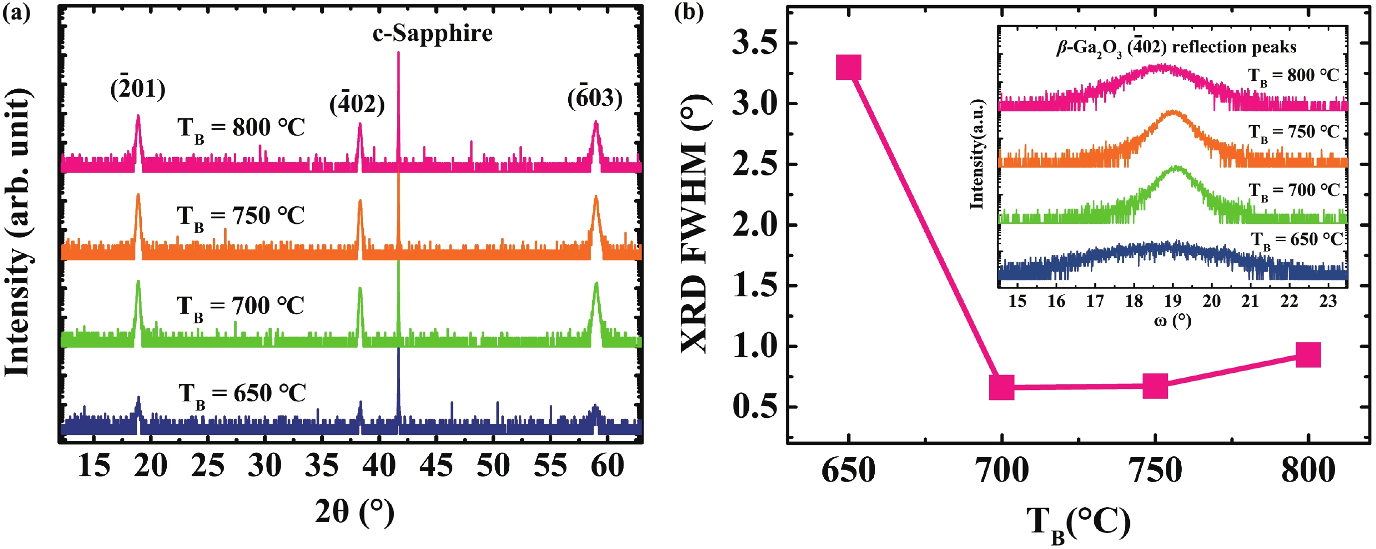
Fig. 1.
(Color online) (a) XRD ω−2θ scan and (b) FWHM of rocking curve for β-Ga2O3 films grown at different TB. Inset shows the XRD ω scan for films.
ARTICLES
Peipei Ma1, 2, Jun Zheng1, 2, , Xiangquan Liu1, 2, Zhi Liu1, 2, Yuhua Zuo1, 2 and Buwen Cheng1, 2
Corresponding author: Jun Zheng, zhengjun@semi.ac.cn
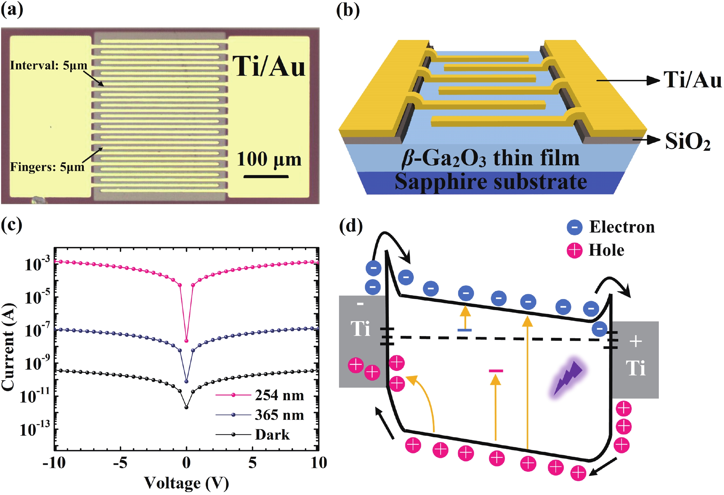
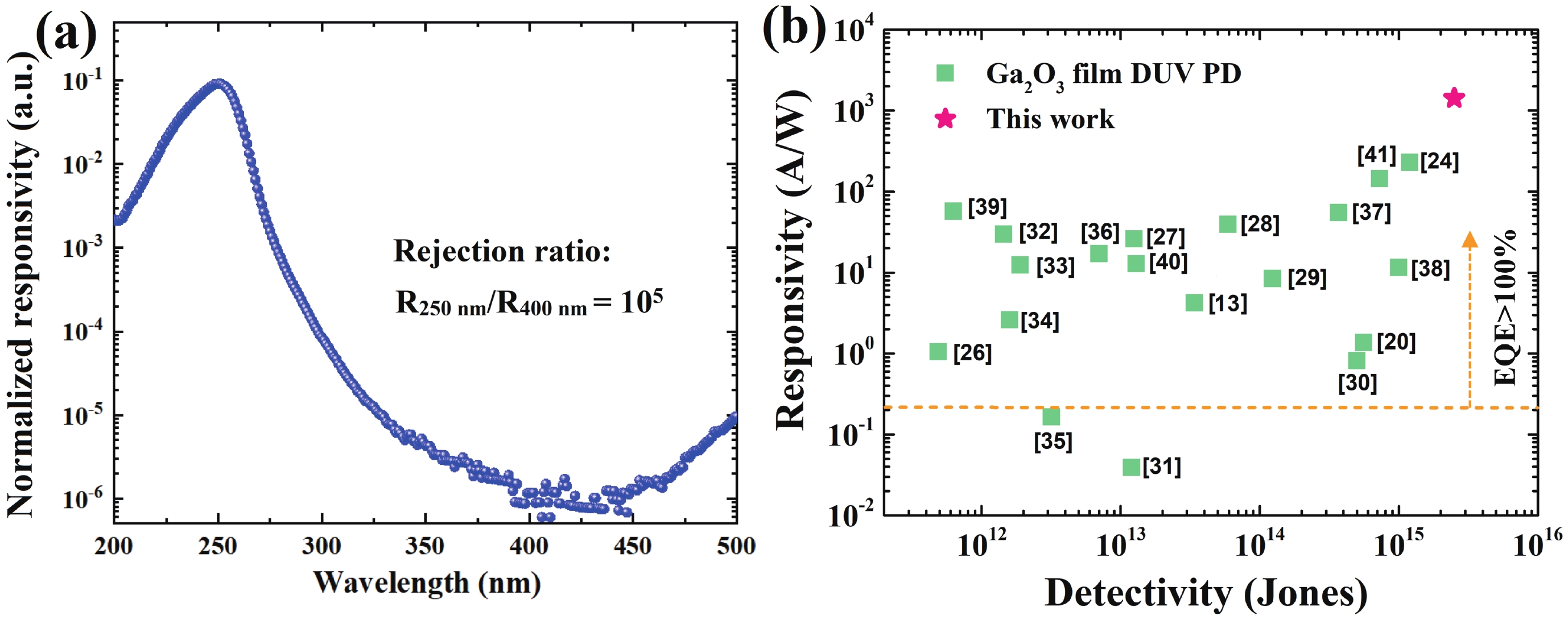
Abstract: In this work, a two-step metal organic chemical vapor deposition (MOCVD) method was applied for growing β-Ga2O3 film on c-plane sapphire. Optimized buffer layer growth temperature (TB) was found at 700 °C and the β-Ga2O3 film with full width at half maximum (FWHM) of 0.66° was achieved. A metal−semiconductor−metal (MSM) solar-blind photodetector (PD) was fabricated based on the β-Ga2O3 film. Ultrahigh responsivity of 1422 A/W @ 254 nm and photo-to-dark current ratio (PDCR) of 106 at 10 V bias were obtained. The detectivity of 2.5 × 10¹⁵ Jones proved that the photodetector has outstanding performance in detecting weak signals. Moreover, the photodetector exhibited superior wavelength selectivity with rejection ratio (R250 nm/R400 nm) of 105. These results indicate that the two-step method is a promising approach for preparation of high-quality β-Ga2O3 films for high-performance solar-blind photodetectors.
Key words: MOCVD, two-step growth, β-Ga2O3, solar-blind photodetector, responsivity
| [1] |
Fu B, Jian G Z, Mu W X, et al. Crystal growth and design of Sn-doped β-Ga2O3: Morphology, defect and property studies of cylindrical crystal by EFG. J Alloys Compd, 2022, 896, 162830 doi: 10.1016/j.jallcom.2021.162830
|
| [2] |
Sun H D, Li K H, Torres Castanedo C G, et al. HCl flow-induced phase change of α-, β-, and ε-Ga2O3 films grown by MOCVD. Cryst Growth Des, 2018, 18, 2370 doi: 10.1021/acs.cgd.7b01791
|
| [3] |
Zhang J C, Dong P F, Dang K, et al. Ultra-wide bandgap semiconductor Ga2O3 power diodes. Nat Commun, 2022, 13, 3900 doi: 10.1038/s41467-022-31664-y
|
| [4] |
Sheoran H, Fang S, Liang F Z, et al. High performance of zero-power-consumption MOCVD-grown β-Ga2O3-based solar-blind photodetectors with ultralow dark current and high-temperature functionalities. ACS Appl Mater Interfaces, 2022, 14, 52096 doi: 10.1021/acsami.2c08511
|
| [5] |
Hou X H, Zhao X L, Zhang Y, et al. High-performance harsh-environment-resistant GaOX solar-blind photodetectors via defect and doping engineering. Adv Mater, 2022, 34, 2106923 doi: 10.1002/adma.202106923
|
| [6] |
Ngo T S, Le D D, Vuong N Q, et al. Systematic investigation of growth and properties of Ga2O3 films on c-plane sapphire substrates prepared by plasma-assisted molecular beam epitaxy. ECS J Solid State Sci Technol, 2022, 11, 035008 doi: 10.1149/2162-8777/ac5d65
|
| [7] |
Murakami H, Nomura K, Goto K, et al. Homoepitaxial growth of β-Ga2O3 layers by halide vapor phase epitaxy. Appl Phys Express, 2015, 8, 015503 doi: 10.7567/APEX.8.015503
|
| [8] |
Saha S, Meng L Y, Feng Z X, et al. Schottky diode characteristics on high-growth rate LPCVD β -Ga2O3 films on (010) and (001) Ga2O3 substrates. Appl Phys Lett, 2022, 120, 122106 doi: 10.1063/5.0083659
|
| [9] |
Rafique S, Han L, Neal A T, et al. Heteroepitaxy of N-type β-Ga2O3 thin films on sapphire substrate by low pressure chemical vapor deposition. Appl Phys Lett, 2016, 109, 132103. doi: 10.1063/1.4963820
|
| [10] |
Xu Y, An Z Y, Zhang L X, et al. Solar blind deep ultraviolet β-Ga2O3 photodetectors grown on sapphire by the Mist-CVD method. Opt Mater Express, 2018, 8, 2941 doi: 10.1364/OME.8.002941
|
| [11] |
Hu D Q, Zhuang S W, Ma Z Z, et al. Study on the optical properties of β-Ga2O3 films grown by MOCVD. J Mater Sci: Mater Electron, 2017, 28, 10997 doi: 10.1007/s10854-017-6882-x
|
| [12] |
Anamika S P, Sriram K, Swanand V S, et al. High responsivity in molecular beam epitaxy grown β-Ga2O3 metal semiconductor metal solar blind deep-UV photodetector. Appl Phys Lett, 2017, 110, 221107 doi: 10.1063/1.4984904
|
| [13] |
Qian L X, Wu Z H, Zhang Y Y, et al. Ultrahigh-responsivity, rapid-recovery, solar-blind photodetector based on highly nonstoichiometric amorphous gallium oxide. ACS Photonics, 2017, 4, 2203 doi: 10.1021/acsphotonics.7b00359
|
| [14] |
Arora K, Goel N, Kumar M, et al. Ultrahigh performance of self-powered β-Ga2O3 thin film solar-blind photodetector grown on cost-effective Si substrate using high-temperature seed layer. ACS Photonics, 2018, 5, 2391 doi: 10.1021/acsphotonics.8b00174
|
| [15] |
Cheng Y L, Zhang C F, Xu Y, et al. Heteroepitaxial growth of β-Ga2O3 thin films on c-plane sapphire substrates with β-(Al x Ga1- x )2O3 intermediate buffer layer by mist-CVD method. Mater Today Commun, 2021, 29, 102766 doi: 10.1016/j.mtcomm.2021.102766
|
| [16] |
Zhang Y B, Zheng J, Ma P P, et al. Growth and characterization of β-Ga2O3 thin films grown on off-angled Al2O3 substrates by metal-organic chemical vapor deposition. J Semicond, 2022, 43, 092801 doi: 10.1088/1674-4926/43/9/092801
|
| [17] |
Ma P P, Zheng J, Zhang Y B, et al. Investigation on n-type (−201) β-Ga2O3 ohmic contact via Si ion implantation. Tsinghua Sci Technol, 2022, 28, 150 doi: 10.26599/TST.2021.9010039
|
| [18] |
Ma P P, Zheng J, Zhang Y B, et al. Lateral β-Ga2O3 Schottky barrier diode fabricated on (–201) single crystal substrate and its temperature-dependent current–voltage characteristics. Chin Phys B, 2022, 31, 047302 doi: 10.1088/1674-1056/ac2729
|
| [19] |
Joshi G, Chauhan Y S, Verma A. Temperature dependence of β-Ga2O3 heteroepitaxy on c-plane sapphire using low pressure chemical vapor deposition. J Alloys Compd, 2021, 883, 160799 doi: 10.1016/j.jallcom.2021.160799
|
| [20] |
Li H R, Wang Y H, Cao J, et al. Enhanced solar-blind photoresponse characteristics in β-Ga2O3 epitaxial films on large miscut sapphire substrates. J Alloys Compd, 2021, 877, 160143 doi: 10.1016/j.jallcom.2021.160143
|
| [21] |
Jiao Y J, Jiang Q, Meng J H, et al. Growth and characteristics of β-Ga2O3 thin films on sapphire (0001) by low pressure chemical vapour deposition. Vacuum, 2021, 189, 110253 doi: 10.1016/j.vacuum.2021.110253
|
| [22] |
Xu W L, Shi J C, Li Y W, et al. Study of β-Ga2O3 films hetero-epitaxially grown on off-angled sapphire substrates by halide vapor phase epitaxy. Mater Lett, 2021, 289, 129411 doi: 10.1016/j.matlet.2021.129411
|
| [23] |
Ma Y J, Tang W B, Chen T W, et al. Effect of off-axis substrate angles on β-Ga2O3 thin films and solar-blind ultraviolet photodetectors grown on sapphire by MOCVD. Mater Sci Semicond Process, 2021, 131, 105856 doi: 10.1016/j.mssp.2021.105856
|
| [24] |
Qin Y A, Li L H, Zhao X L, et al. Metal–semiconductor–metal ε-Ga2O3 solar-blind photodetectors with a record-high responsivity rejection ratio and their gain mechanism. ACS Photonics, 2020, 7, 812 doi: 10.1021/acsphotonics.9b01727
|
| [25] |
Kim S, Kim J. Highly selective ozone-treated β-Ga2O3 solar-blind deep-UV photodetectors. Appl Phys Lett, 2020, 117, 261101 doi: 10.1063/5.0030400
|
| [26] |
Li Y Q, Zhang D, Lin R C, et al. Graphene interdigital electrodes for improving sensitivity in a Ga2O3: Zn deep-ultraviolet photoconductive detector. ACS Appl Mater Interfaces, 2019, 11, 1013 doi: 10.1021/acsami.8b14380
|
| [27] |
Zhang D, Zheng W, Lin R C, et al. High quality β-Ga2O3 film grown with N2O for high sensitivity solar-blind-ultraviolet photodetector with fast response speed. J Alloys Compd, 2018, 735, 150 doi: 10.1016/j.jallcom.2017.11.037
|
| [28] |
Kong W Y, Wu G A, Wang K Y, et al. Graphene- β-Ga2O3 heterojunction for highly sensitive deep UV photodetector application. Adv Mater, 2016, 28, 10725 doi: 10.1002/adma.201604049
|
| [29] |
Qian L X, Liu H Y, Zhang H F, et al. Simultaneously improved sensitivity and response speed of β-Ga2O3 solar-blind photodetector via localized tuning of oxygen deficiency. Appl Phys Lett, 2019, 114, 113506 doi: 10.1063/1.5088665
|
| [30] |
Wang Y H, Cui W J, Yu J E, et al. One-step growth of amorphous/crystalline Ga2O3 phase junctions for high-performance solar-blind photodetection. ACS Appl Mater Interfaces, 2019, 11, 45922 doi: 10.1021/acsami.9b17409
|
| [31] |
Zhou H T, Cong L J, Ma J G, et al. High-performance high-temperature solar-blind photodetector based on polycrystalline Ga2O3 film. J Alloys Compd, 2020, 847, 156536 doi: 10.1016/j.jallcom.2020.156536
|
| [32] |
Oh S, Kim C K, Kim J. High responsivity β-Ga2O3 metal–semiconductor–metal solar-blind photodetectors with ultraviolet transparent graphene electrodes. ACS Photonics, 2018, 5, 1123 doi: 10.1021/acsphotonics.7b01486
|
| [33] |
Chen Y C, Lu Y J, Liu Q, et al. Ga2O3 photodetector arrays for solar-blind imaging. J Mater Chem C, 2019, 7, 2557 doi: 10.1039/C8TC05251D
|
| [34] |
Li M Q, Yang N, Wang G G, et al. Highly preferred orientation of Ga2O3 films sputtered on SiC substrates for deep UV photodetector application. Appl Surf Sci, 2019, 471, 694 doi: 10.1016/j.apsusc.2018.12.045
|
| [35] |
Li Y N, Li Y Q, Ji Y, et al. Sol-gel preparation of Sn doped gallium oxide films for application in solar-blind ultraviolet photodetectors. J Mater Sci, 2022, 57, 1186 doi: 10.1007/s10853-021-06680-w
|
| [36] |
Hu G C, Shan C X, Zhang N, et al. High gain Ga2O3 solar-blind photodetectors realized via a carrier multiplication process. Opt Express, 2015, 23, 13554 doi: 10.1364/OE.23.013554
|
| [37] |
Qian L X, Zhang H F, Lai P T, et al. High-sensitivity β-Ga2O3 solar-blind photodetector on high-temperature pretreated c-plane sapphire substrate. Opt Mater Express, 2017, 7, 3643 doi: 10.1364/OME.7.003643
|
| [38] |
Hou X H, Sun H D, Long S B, et al. Ultrahigh-performance solar-blind photodetector based on α-phase- dominated Ga2O3 film with record low dark current of 81 fA. IEEE Electron Device Lett, 2019, 40, 1483 doi: 10.1109/LED.2019.2932140
|
| [39] |
Pintor-Monroy M I, Murillo-Borjas B L, Quevedo-Lopez M A. Nanocrystalline and polycrystalline β-Ga2O3 thin films for deep ultraviolet detectors. ACS Appl Electron Mater, 2020, 2, 3358 doi: 10.1021/acsaelm.0c00643
|
| [40] |
Lin R C, Zheng W, Zhang D, et al. High-performance graphene/β-Ga2O3 heterojunction deep-ultraviolet photodetector with hot-electron excited carrier multiplication. ACS Appl Mater Interfaces, 2018, 10, 22419 doi: 10.1021/acsami.8b05336
|
| [41] |
Liu Z, Wang X A, Liu Y Y, et al. A high-performance ultraviolet solar-blind photodetector based on a β-Ga2O3 Schottky photodiode. J Mater Chem C, 2019, 7, 13920 doi: 10.1039/C9TC04912F
|


Article views: 666 Times PDF downloads: 106 Times Cited by: 0 Times
Received: 12 September 2023 Revised: 31 October 2023 Online: Accepted Manuscript: 29 November 2023Uncorrected proof: 08 December 2023Published: 10 February 2024
| Citation: |
Peipei Ma, Jun Zheng, Xiangquan Liu, Zhi Liu, Yuhua Zuo, Buwen Cheng. Two-step growth of β-Ga2O3 on c-plane sapphire using MOCVD for solar-blind photodetector[J]. Journal of Semiconductors, 2024, 45(2): 022502. doi: 10.1088/1674-4926/45/2/022502
P P Ma, J Zheng, X Q Liu, Z Liu, Y H Zuo, B W Cheng. Two-step growth of β-Ga2O3 on c-plane sapphire using MOCVD for solar-blind photodetector[J]. J. Semicond, 2024, 45(2): 022502. doi: 10.1088/1674-4926/45/2/022502
Export: BibTex EndNote

|
| [1] |
Fu B, Jian G Z, Mu W X, et al. Crystal growth and design of Sn-doped β-Ga2O3: Morphology, defect and property studies of cylindrical crystal by EFG. J Alloys Compd, 2022, 896, 162830 doi: 10.1016/j.jallcom.2021.162830
|
| [2] |
Sun H D, Li K H, Torres Castanedo C G, et al. HCl flow-induced phase change of α-, β-, and ε-Ga2O3 films grown by MOCVD. Cryst Growth Des, 2018, 18, 2370 doi: 10.1021/acs.cgd.7b01791
|
| [3] |
Zhang J C, Dong P F, Dang K, et al. Ultra-wide bandgap semiconductor Ga2O3 power diodes. Nat Commun, 2022, 13, 3900 doi: 10.1038/s41467-022-31664-y
|
| [4] |
Sheoran H, Fang S, Liang F Z, et al. High performance of zero-power-consumption MOCVD-grown β-Ga2O3-based solar-blind photodetectors with ultralow dark current and high-temperature functionalities. ACS Appl Mater Interfaces, 2022, 14, 52096 doi: 10.1021/acsami.2c08511
|
| [5] |
Hou X H, Zhao X L, Zhang Y, et al. High-performance harsh-environment-resistant GaOX solar-blind photodetectors via defect and doping engineering. Adv Mater, 2022, 34, 2106923 doi: 10.1002/adma.202106923
|
| [6] |
Ngo T S, Le D D, Vuong N Q, et al. Systematic investigation of growth and properties of Ga2O3 films on c-plane sapphire substrates prepared by plasma-assisted molecular beam epitaxy. ECS J Solid State Sci Technol, 2022, 11, 035008 doi: 10.1149/2162-8777/ac5d65
|
| [7] |
Murakami H, Nomura K, Goto K, et al. Homoepitaxial growth of β-Ga2O3 layers by halide vapor phase epitaxy. Appl Phys Express, 2015, 8, 015503 doi: 10.7567/APEX.8.015503
|
| [8] |
Saha S, Meng L Y, Feng Z X, et al. Schottky diode characteristics on high-growth rate LPCVD β -Ga2O3 films on (010) and (001) Ga2O3 substrates. Appl Phys Lett, 2022, 120, 122106 doi: 10.1063/5.0083659
|
| [9] |
Rafique S, Han L, Neal A T, et al. Heteroepitaxy of N-type β-Ga2O3 thin films on sapphire substrate by low pressure chemical vapor deposition. Appl Phys Lett, 2016, 109, 132103. doi: 10.1063/1.4963820
|
| [10] |
Xu Y, An Z Y, Zhang L X, et al. Solar blind deep ultraviolet β-Ga2O3 photodetectors grown on sapphire by the Mist-CVD method. Opt Mater Express, 2018, 8, 2941 doi: 10.1364/OME.8.002941
|
| [11] |
Hu D Q, Zhuang S W, Ma Z Z, et al. Study on the optical properties of β-Ga2O3 films grown by MOCVD. J Mater Sci: Mater Electron, 2017, 28, 10997 doi: 10.1007/s10854-017-6882-x
|
| [12] |
Anamika S P, Sriram K, Swanand V S, et al. High responsivity in molecular beam epitaxy grown β-Ga2O3 metal semiconductor metal solar blind deep-UV photodetector. Appl Phys Lett, 2017, 110, 221107 doi: 10.1063/1.4984904
|
| [13] |
Qian L X, Wu Z H, Zhang Y Y, et al. Ultrahigh-responsivity, rapid-recovery, solar-blind photodetector based on highly nonstoichiometric amorphous gallium oxide. ACS Photonics, 2017, 4, 2203 doi: 10.1021/acsphotonics.7b00359
|
| [14] |
Arora K, Goel N, Kumar M, et al. Ultrahigh performance of self-powered β-Ga2O3 thin film solar-blind photodetector grown on cost-effective Si substrate using high-temperature seed layer. ACS Photonics, 2018, 5, 2391 doi: 10.1021/acsphotonics.8b00174
|
| [15] |
Cheng Y L, Zhang C F, Xu Y, et al. Heteroepitaxial growth of β-Ga2O3 thin films on c-plane sapphire substrates with β-(Al x Ga1- x )2O3 intermediate buffer layer by mist-CVD method. Mater Today Commun, 2021, 29, 102766 doi: 10.1016/j.mtcomm.2021.102766
|
| [16] |
Zhang Y B, Zheng J, Ma P P, et al. Growth and characterization of β-Ga2O3 thin films grown on off-angled Al2O3 substrates by metal-organic chemical vapor deposition. J Semicond, 2022, 43, 092801 doi: 10.1088/1674-4926/43/9/092801
|
| [17] |
Ma P P, Zheng J, Zhang Y B, et al. Investigation on n-type (−201) β-Ga2O3 ohmic contact via Si ion implantation. Tsinghua Sci Technol, 2022, 28, 150 doi: 10.26599/TST.2021.9010039
|
| [18] |
Ma P P, Zheng J, Zhang Y B, et al. Lateral β-Ga2O3 Schottky barrier diode fabricated on (–201) single crystal substrate and its temperature-dependent current–voltage characteristics. Chin Phys B, 2022, 31, 047302 doi: 10.1088/1674-1056/ac2729
|
| [19] |
Joshi G, Chauhan Y S, Verma A. Temperature dependence of β-Ga2O3 heteroepitaxy on c-plane sapphire using low pressure chemical vapor deposition. J Alloys Compd, 2021, 883, 160799 doi: 10.1016/j.jallcom.2021.160799
|
| [20] |
Li H R, Wang Y H, Cao J, et al. Enhanced solar-blind photoresponse characteristics in β-Ga2O3 epitaxial films on large miscut sapphire substrates. J Alloys Compd, 2021, 877, 160143 doi: 10.1016/j.jallcom.2021.160143
|
| [21] |
Jiao Y J, Jiang Q, Meng J H, et al. Growth and characteristics of β-Ga2O3 thin films on sapphire (0001) by low pressure chemical vapour deposition. Vacuum, 2021, 189, 110253 doi: 10.1016/j.vacuum.2021.110253
|
| [22] |
Xu W L, Shi J C, Li Y W, et al. Study of β-Ga2O3 films hetero-epitaxially grown on off-angled sapphire substrates by halide vapor phase epitaxy. Mater Lett, 2021, 289, 129411 doi: 10.1016/j.matlet.2021.129411
|
| [23] |
Ma Y J, Tang W B, Chen T W, et al. Effect of off-axis substrate angles on β-Ga2O3 thin films and solar-blind ultraviolet photodetectors grown on sapphire by MOCVD. Mater Sci Semicond Process, 2021, 131, 105856 doi: 10.1016/j.mssp.2021.105856
|
| [24] |
Qin Y A, Li L H, Zhao X L, et al. Metal–semiconductor–metal ε-Ga2O3 solar-blind photodetectors with a record-high responsivity rejection ratio and their gain mechanism. ACS Photonics, 2020, 7, 812 doi: 10.1021/acsphotonics.9b01727
|
| [25] |
Kim S, Kim J. Highly selective ozone-treated β-Ga2O3 solar-blind deep-UV photodetectors. Appl Phys Lett, 2020, 117, 261101 doi: 10.1063/5.0030400
|
| [26] |
Li Y Q, Zhang D, Lin R C, et al. Graphene interdigital electrodes for improving sensitivity in a Ga2O3: Zn deep-ultraviolet photoconductive detector. ACS Appl Mater Interfaces, 2019, 11, 1013 doi: 10.1021/acsami.8b14380
|
| [27] |
Zhang D, Zheng W, Lin R C, et al. High quality β-Ga2O3 film grown with N2O for high sensitivity solar-blind-ultraviolet photodetector with fast response speed. J Alloys Compd, 2018, 735, 150 doi: 10.1016/j.jallcom.2017.11.037
|
| [28] |
Kong W Y, Wu G A, Wang K Y, et al. Graphene- β-Ga2O3 heterojunction for highly sensitive deep UV photodetector application. Adv Mater, 2016, 28, 10725 doi: 10.1002/adma.201604049
|
| [29] |
Qian L X, Liu H Y, Zhang H F, et al. Simultaneously improved sensitivity and response speed of β-Ga2O3 solar-blind photodetector via localized tuning of oxygen deficiency. Appl Phys Lett, 2019, 114, 113506 doi: 10.1063/1.5088665
|
| [30] |
Wang Y H, Cui W J, Yu J E, et al. One-step growth of amorphous/crystalline Ga2O3 phase junctions for high-performance solar-blind photodetection. ACS Appl Mater Interfaces, 2019, 11, 45922 doi: 10.1021/acsami.9b17409
|
| [31] |
Zhou H T, Cong L J, Ma J G, et al. High-performance high-temperature solar-blind photodetector based on polycrystalline Ga2O3 film. J Alloys Compd, 2020, 847, 156536 doi: 10.1016/j.jallcom.2020.156536
|
| [32] |
Oh S, Kim C K, Kim J. High responsivity β-Ga2O3 metal–semiconductor–metal solar-blind photodetectors with ultraviolet transparent graphene electrodes. ACS Photonics, 2018, 5, 1123 doi: 10.1021/acsphotonics.7b01486
|
| [33] |
Chen Y C, Lu Y J, Liu Q, et al. Ga2O3 photodetector arrays for solar-blind imaging. J Mater Chem C, 2019, 7, 2557 doi: 10.1039/C8TC05251D
|
| [34] |
Li M Q, Yang N, Wang G G, et al. Highly preferred orientation of Ga2O3 films sputtered on SiC substrates for deep UV photodetector application. Appl Surf Sci, 2019, 471, 694 doi: 10.1016/j.apsusc.2018.12.045
|
| [35] |
Li Y N, Li Y Q, Ji Y, et al. Sol-gel preparation of Sn doped gallium oxide films for application in solar-blind ultraviolet photodetectors. J Mater Sci, 2022, 57, 1186 doi: 10.1007/s10853-021-06680-w
|
| [36] |
Hu G C, Shan C X, Zhang N, et al. High gain Ga2O3 solar-blind photodetectors realized via a carrier multiplication process. Opt Express, 2015, 23, 13554 doi: 10.1364/OE.23.013554
|
| [37] |
Qian L X, Zhang H F, Lai P T, et al. High-sensitivity β-Ga2O3 solar-blind photodetector on high-temperature pretreated c-plane sapphire substrate. Opt Mater Express, 2017, 7, 3643 doi: 10.1364/OME.7.003643
|
| [38] |
Hou X H, Sun H D, Long S B, et al. Ultrahigh-performance solar-blind photodetector based on α-phase- dominated Ga2O3 film with record low dark current of 81 fA. IEEE Electron Device Lett, 2019, 40, 1483 doi: 10.1109/LED.2019.2932140
|
| [39] |
Pintor-Monroy M I, Murillo-Borjas B L, Quevedo-Lopez M A. Nanocrystalline and polycrystalline β-Ga2O3 thin films for deep ultraviolet detectors. ACS Appl Electron Mater, 2020, 2, 3358 doi: 10.1021/acsaelm.0c00643
|
| [40] |
Lin R C, Zheng W, Zhang D, et al. High-performance graphene/β-Ga2O3 heterojunction deep-ultraviolet photodetector with hot-electron excited carrier multiplication. ACS Appl Mater Interfaces, 2018, 10, 22419 doi: 10.1021/acsami.8b05336
|
| [41] |
Liu Z, Wang X A, Liu Y Y, et al. A high-performance ultraviolet solar-blind photodetector based on a β-Ga2O3 Schottky photodiode. J Mater Chem C, 2019, 7, 13920 doi: 10.1039/C9TC04912F
|

 WeChat ID
Journal of Semiconductors © 2017 All Rights Reserved 京ICP备05085259号-2

 DownLoad:

