| [1] |
Novoselov K S, Geim A K, Morozov S V, et al. Electric field effect in atomically thin carbon films. Science, 2004, 306, 666 doi: 10.1126/science.1102896 |
| [2] |
Liu H, Neal A T, Zhu Z, et al. Phosphorene: An unexplored 2D semiconductor with a high hole mobility. ACS Nano, 2014, 8, 4033 doi: 10.1021/nn501226z |
| [3] |
Hu Y, Liang J, Xia Y, et al. 2D arsenene and arsenic materials: Fundamental properties, preparation, and applications. Small, 2022, 18, e2104556 doi: 10.1002/smll.202104556 |
| [4] |
Ji J, Song X, Liu J, et al. Two-dimensional antimonene single crystals grown by van der Waals epitaxy. Nat Commun, 2016, 7, 13352 doi: 10.1038/ncomms13352 |
| [5] |
Pumera M, Sofer Z. 2D monoelemental arsenene, antimonene, and bismuthene: Beyond black phosphorus. Adv Mater, 2017, 29, 1605299 doi: 10.1002/adma.201605299 |
| [6] |
Shirotani I, Kawamura H, Tuburaya K, et al. Superconductivity of phosphorus and phosphorus-arsenic alloy under high pressures. Jpn J Appl Phys, 1987, 26, 921 doi: 10.7567/JJAPS.26S3.921 |
| [7] |
Osters O, Nilges T, Bachhuber F, et al. Synthesis and identification of metastable compounds: black arsenic-science or fiction? Angew Chem Int Ed Engl, 2012, 51, 2994 doi: 10.1002/anie.201106479 |
| [8] |
Liu B L, Köpf M, Abbas A N, et al. Black arsenic-phosphorus: Layered anisotropic infrared semiconductors with highly tunable compositions and properties. Adv Mater, 2015, 27, 4423 doi: 10.1002/adma.201501758 |
| [9] |
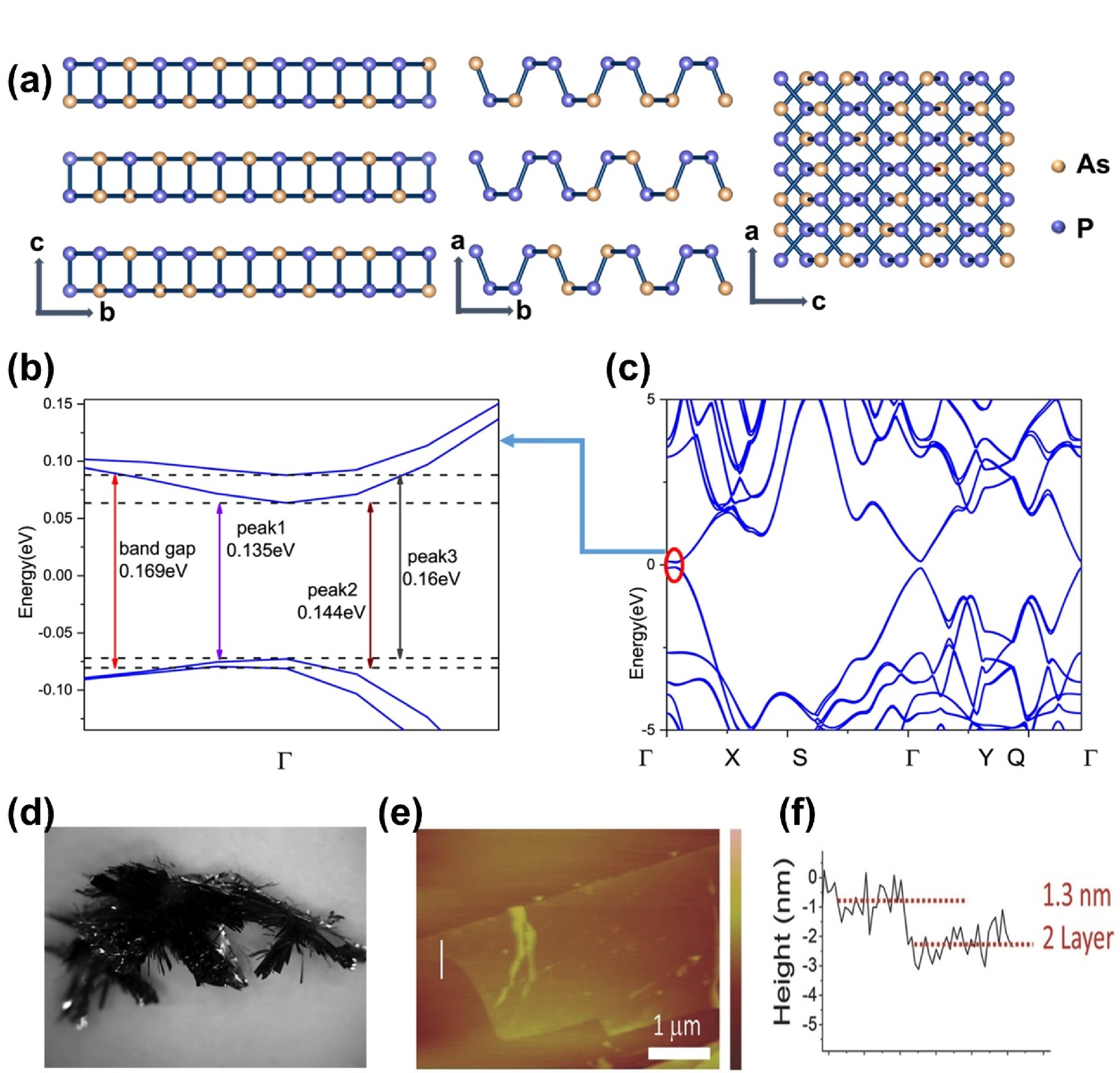
Xie M, Zhang S, Cai B, et al. A promising two-dimensional solar cell donor: Black arsenic–phosphorus monolayer with 1.54 eV direct bandgap and mobility exceeding 14, 000 cm 2V −1s −1. Nano Energy, 2016, 28, 433 doi: 10.1016/j.nanoen.2016.08.058 |
| [10] |
Sun J, Lin N, Ren H, et al. The electronic structure, mechanical flexibility and carrier mobility of black arsenic-phosphorus monolayers: a first principles study. Phys Chem Chem Phys, 2016, 18, 9779 doi: 10.1039/C6CP00047A |
| [11] |
Shi X Y, Wang T, Wang J, et al. Synthesis of black arsenic-phosphorus and its application for Er-doped fiber ultrashort laser generation. Opt Mater Express, 2019, 9, 2348 doi: 10.1364/OME.9.002348 |
| [12] |
Young E P, Park J, Bai T Y, et al. Wafer-scale black arsenic–phosphorus thin-film synthesis validated with density functional perturbation theory predictions. ACS Appl Nano Mater, 2018, 1, 4737 doi: 10.1021/acsanm.8b00951 |
| [13] |
Yuan S F, Shen C F, Deng B C, et al. Air-stable room-temperature mid-infrared photodetectors based on hBN/black arsenic phosphorus/hBN heterostructures. Nano Lett, 2018, 18, 3172 doi: 10.1021/acs.nanolett.8b00835 |
| [14] |
Long M S, Gao A Y, Wang P, et al. Room temperature high-detectivity mid-infrared photodetectors based on black arsenic phosphorus. Sci Adv, 2017, 3, e1700589 doi: 10.1126/sciadv.1700589 |
| [15] |
Zhou W H, Zhang S L, Wang Y Y, et al. Anisotropic in-plane ballistic transport in monolayer black arsenic-phosphorus FETs. Adv Elect Materials, 2020, 6, 1901281 doi: 10.1002/aelm.201901281 |
| [16] |
Luxa J, Bouša D, Zoller F, et al. Black phosphorus–arsenic alloys for lithium ion batteries. FlatChem, 2020, 19, 100143 doi: 10.1016/j.flatc.2019.100143 |
| [17] |
Yu L, Zhu Z, Gao A Y, et al. Electrically tunable optical properties of few-layer black arsenic phosphorus. Nanotechnology, 2018, 29, 484001 doi: 10.1088/1361-6528/aae05f |


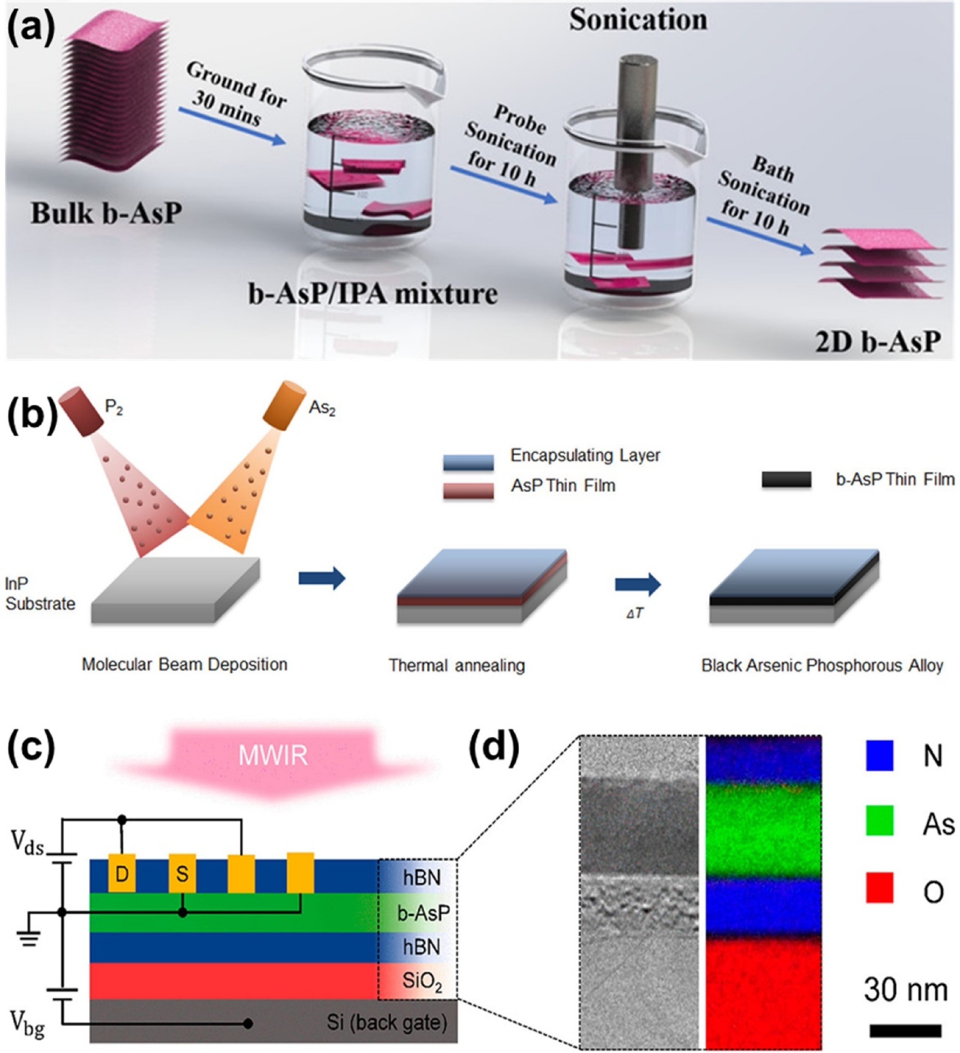
 DownLoad: