


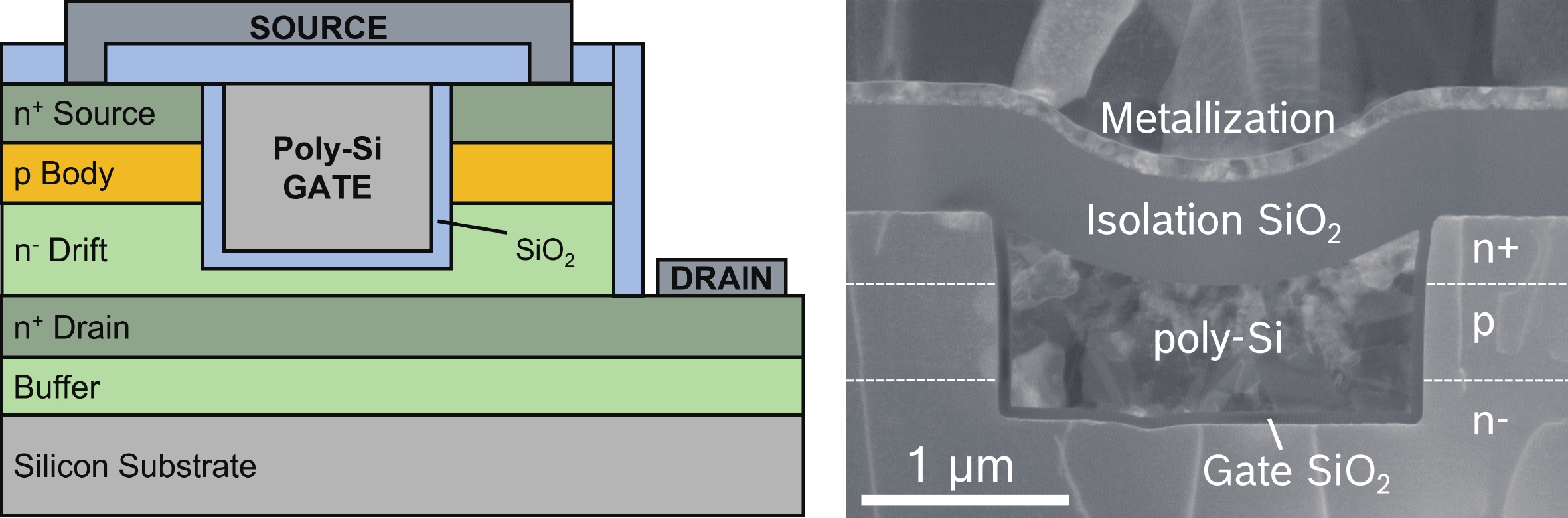
Fig. 1.
(Color online) (a) Schematic 2-D view of the pseudo-vertical GaN-on-Si TMOS under study in this work. (b) TEM image of a FIB lamella taken from the gate trench.
ARTICLES
Nicolò Zagni1, , Manuel Fregolent2, , Andrea Del Fiol2, Davide Favero2, Francesco Bergamin2, Giovanni Verzellesi3, 4, Carlo De Santi2, Gaudenzio Meneghesso2, Enrico Zanoni2, Christian Huber5, Matteo Meneghini2 and Paolo Pavan1
Corresponding author: Nicolò Zagni, nicolo.zagni@unimore.it; Manuel Fregolent, fregolentm@dei.unipd.it
Abstract: Vertical GaN power MOSFET is a novel technology that offers great potential for power switching applications. Being still in an early development phase, vertical GaN devices are yet to be fully optimized and require careful studies to foster their development. In this work, we report on the physical insights into device performance improvements obtained during the development of vertical GaN-on-Si trench MOSFETs (TMOS’s) provided by TCAD simulations, enhancing the dependability of the adopted process optimization approaches. Specifically, two different TMOS devices are compared in terms of transfer-curve hysteresis (H) and subthreshold slope (SS), showing a ≈ 75% H reduction along with a ≈ 30% SS decrease. Simulations allow attributing the achieved improvements to a decrease in the border and interface traps, respectively. A sensitivity analysis is also carried out, allowing to quantify the additional trap density reduction required to minimize both figures of merit.
Key words: vertical GaN trench MOSFET, SiO2, interface traps, border traps, hysteresis, BTI
| [1] |
Fu H Q, Fu K, Chowdhury S, et al. Vertical GaN power devices: Device principles and fabrication technologies—Part II. IEEE Trans Electron Devices, 2021, 68, 3212 doi: 10.1109/TED.2021.3083209
|
| [2] |
Meneghini M, De Santi C, Abid I, et al. GaN-based power devices: Physics, reliability, and perspectives. J Appl Phys, 2021, 130, 181101 doi: 10.1063/5.0061354
|
| [3] |
del Alamo J A, Lee E S. Stability and reliability of lateral GaN power field-effect transistors. IEEE Trans Electron Devices, 2019, 66, 4578 doi: 10.1109/TED.2019.2931718
|
| [4] |
Zagni N, Chini A, Puglisi F M, et al. “hole redistribution” model explaining the thermally activated RON stress/recovery transients in carbon-doped AlGaN/GaN power MIS-HEMTs. IEEE Trans Electron Devices, 2021, 68, 697 doi: 10.1109/TED.2020.3045683
|
| [5] |
Cioni M, Zagni N, Iucolano F, et al. Partial recovery of dynamic RON versus OFF-state stress voltage in p-GaN gate AlGaN/GaN power HEMTs. IEEE Trans Electron Devices, 2021, 68, 4862 doi: 10.1109/TED.2021.3105075
|
| [6] |
Chini A, Meneghesso G, Meneghini M, et al. Experimental and numerical analysis of hole emission process from carbon-related traps in GaN buffer layers. IEEE Trans Electron Devices, 2016, 63, 3473 doi: 10.1109/TED.2016.2593791
|
| [7] |
Modolo N, De Santi C, Minetto A, et al. A physics-based approach to model hot-electron trapping kinetics in p-GaN HEMTs. IEEE Electron Device Lett, 2021, 42, 673 doi: 10.1109/LED.2021.3067796
|
| [8] |
Ohnishi K, Kawasaki S, Fujimoto N, et al. Vertical GaN p+-n junction diode with ideal avalanche capability grown by halide vapor phase epitaxy. Appl Phys Lett, 2021, 119, 152102 doi: 10.1063/5.0066139
|
| [9] |
Bian Z L, Zeng K, Chowdhury S. 2.8 kV avalanche in vertical GaN PN diode utilizing field plate on hydrogen passivated P-layer. IEEE Electron Device Lett, 2022, 43, 596 doi: 10.1109/LED.2022.3149748
|
| [10] |
Liu J, Xiao M, Zhang Y, et al. 1.2 kV vertical GaN fin JFETs with robust avalanche and fast switching capabilities. 2020 IEEE International Electron Devices Meeting (IEDM), San Francisco, CA, USA. IEEE, 2021, 23.2. 1 doi: 10.1109/IEDM13553.2020.9372048
|
| [11] |
Mukherjee K, De Santi C, Borga M, et al. Challenges and perspectives for vertical GaN-on-Si trench MOS reliability: From leakage current analysis to gate stack optimization. Materials, 2021, 14, 2316 doi: 10.3390/ma14092316
|
| [12] |
Treidel E B, Hilt O, Hoffmann V, et al. On the conduction properties of vertical GaN n-channel trench MISFETs. IEEE J Electron Devices Soc, 2021, 9, 215 doi: 10.1109/JEDS.2021.3056697
|
| [13] |
Mukherjee K, De Santi C, Borga M, et al. Use of bilayer gate insulator in GaN-on-Si vertical trench MOSFETs: Impact on performance and reliability. Materials, 2020, 13, 4740 doi: 10.3390/ma13214740
|
| [14] |
Dannecker K, Baringhaus J. Fully vertical gallium nitride trench MOSFETs fabricated with metal-free gate first process. J Vac Sci Technol B, 2021, 39, 032204 doi: 10.1116/6.0000980
|
| [15] |
Henn M, Huber C. Impact of gate dielectric deposition temperature on p-type inversion channel MOSFETs fabricated on GaN-on-Si. 2022 IEEE Workshop on Wide Bandgap Power Devices and Applications in Europe (WiPDA Europe), 2022, 1 doi: 10.1109/WiPDAEurope55971.2022.9936574
|
| [16] |
Pavan P, Zagni N, Puglisi F M, et al. The impact of interface and border traps on current–voltage, capacitance–voltage, and split-CV mobility measurements in InGaAs MOSFETs. Phys Status Solidi A, 2017, 214, 1600592 doi: 10.1002/pssa.201600592
|
| [17] |
Guo A, del Alamo J A. Unified mechanism for positive- and negative-bias temperature instability in GaN MOSFETs. IEEE Trans Electron Devices, 2017, 64, 2142 doi: 10.1109/TED.2017.2686840
|
| [18] |
Wu T L, Franco J, Marcon D, et al. Toward understanding positive bias temperature instability in fully recessed-gate GaN MISFETs. IEEE Trans Electron Devices, 2016, 63, 1853 doi: 10.1109/TED.2016.2539341
|
| [19] |
Lagger P, Reiner M, Pogany D, et al. Comprehensive study of the complex dynamics of forward bias-induced threshold voltage drifts in GaN based MIS-HEMTs by stress/recovery experiments. IEEE Trans Electron Devices, 2014, 61, 1022 doi: 10.1109/TED.2014.2303853
|
| [20] |
Fregolent M, Del Fiol A, De Santi C, et al. Threshold voltage instability in SiO2-gate semi-vertical GaN trench MOSFETs grown on silicon substrate. Microelectron Reliab, 2023, 150, 115130 doi: 10.1016/j.microrel.2023.115130
|
| [21] |
Synopsys. Sentaurus SDevice manual (S-2021.06), 2021
|
| [22] |
Schroder D K. Oxide and interface trapped charges, oxide thickness. John Wiley & Sons, Inc. , 2005, 319
|
| [23] |
Sze S M, Ng K K. Physics of semiconductor devices. John Wiley & Sons, Inc. , 2006
|
| [24] |
Yu M Z, McNab S, Al-Dhahir I, et al. Extracting band-tail interface state densities from measurements and modelling of space charge layer resistance. Sol Energy Mater Sol Cells, 2021, 231, 111307 doi: 10.1016/j.solmat.2021.111307
|
| [25] |
Selmi L, Caruso E, Carapezzi S, et al. Modelling nanoscale n-MOSFETs with III-V compound semiconductor channels: From advanced models for band structures, electrostatics and transport to TCAD. 2017 IEEE International Electron Devices Meeting (IEDM), 2018, 13.4. 1 doi: 10.1109/IEDM.2017.8268384
|
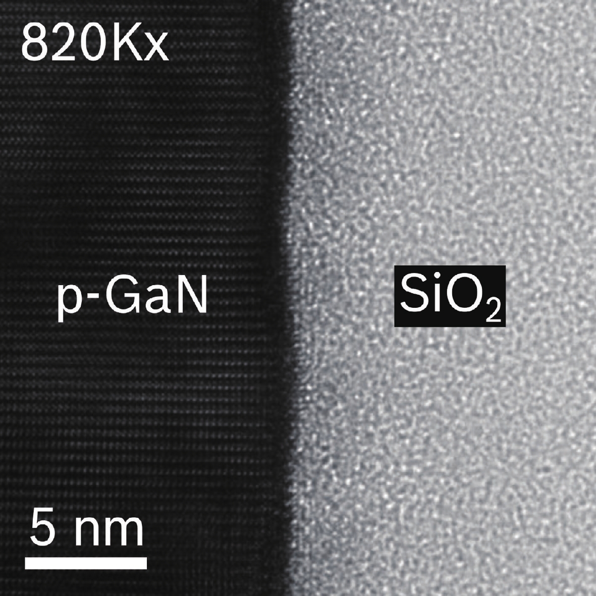

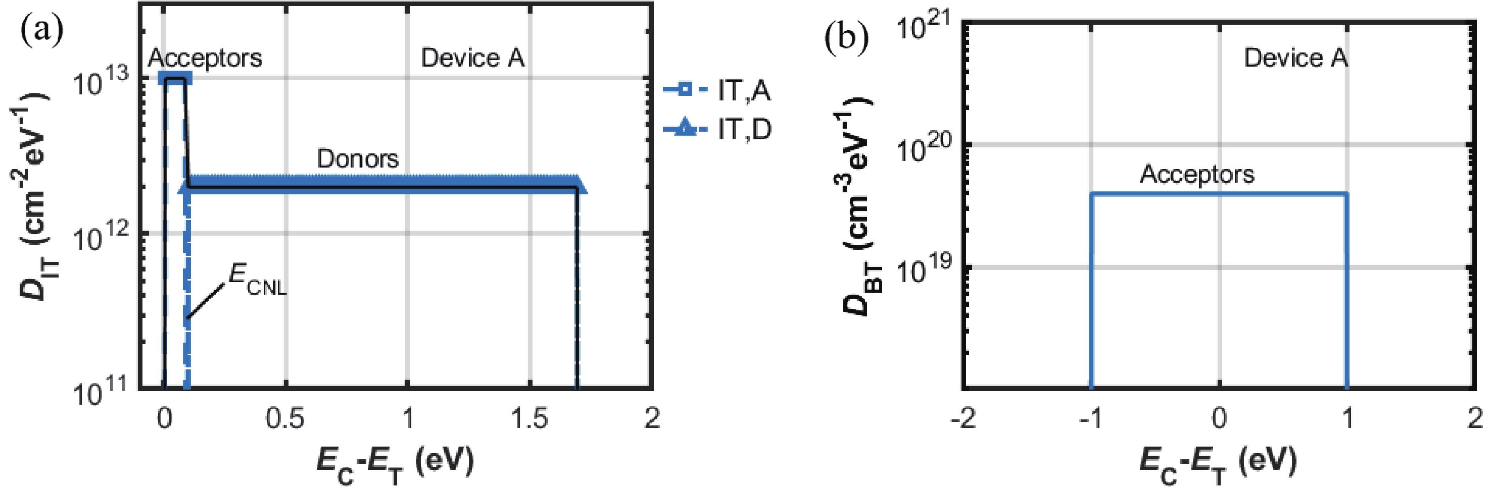
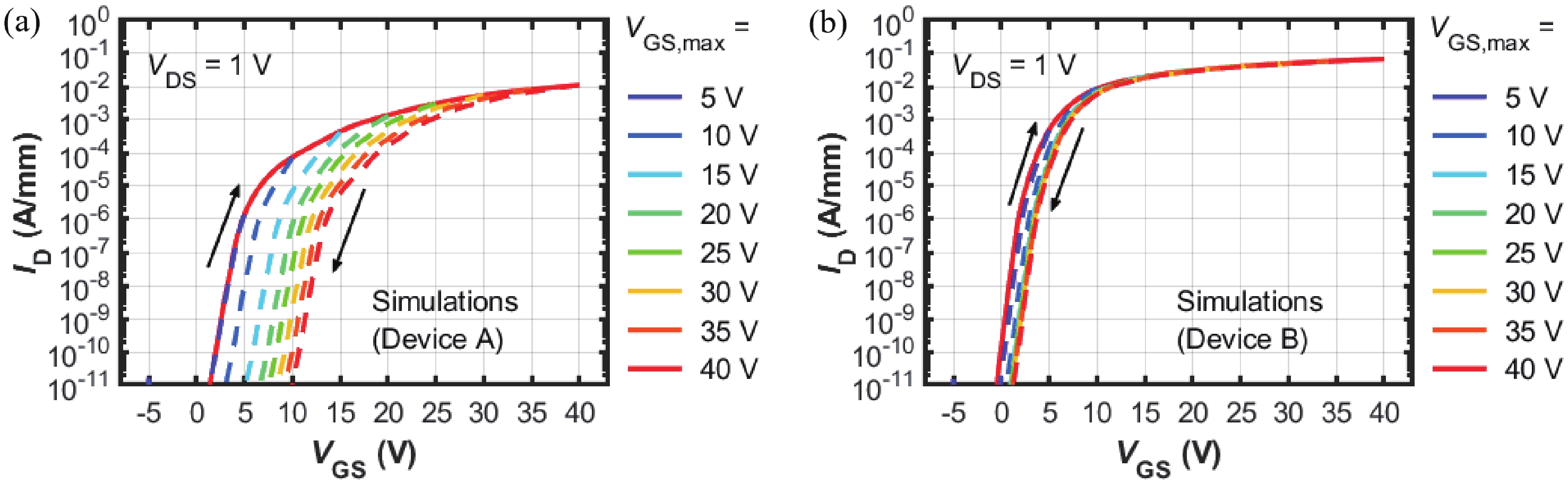

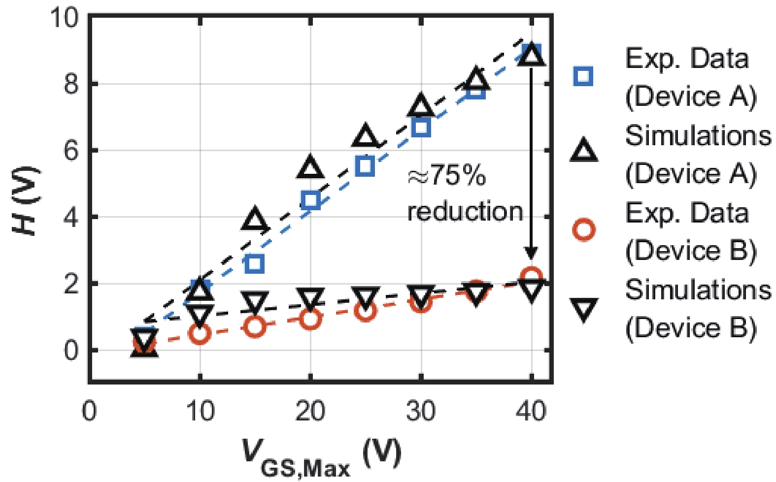
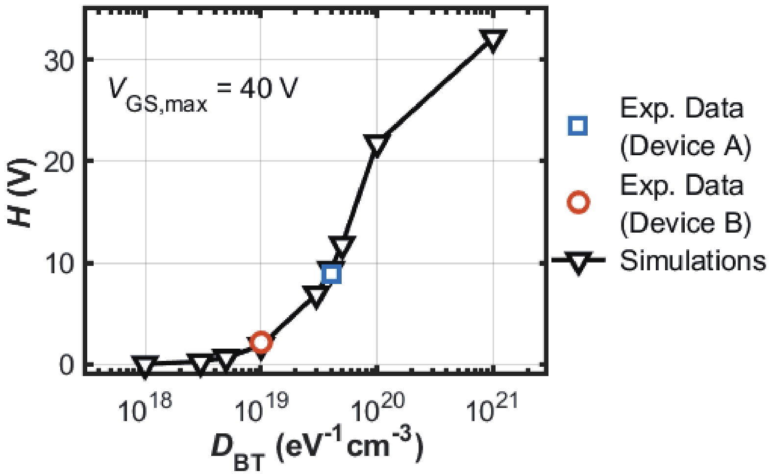
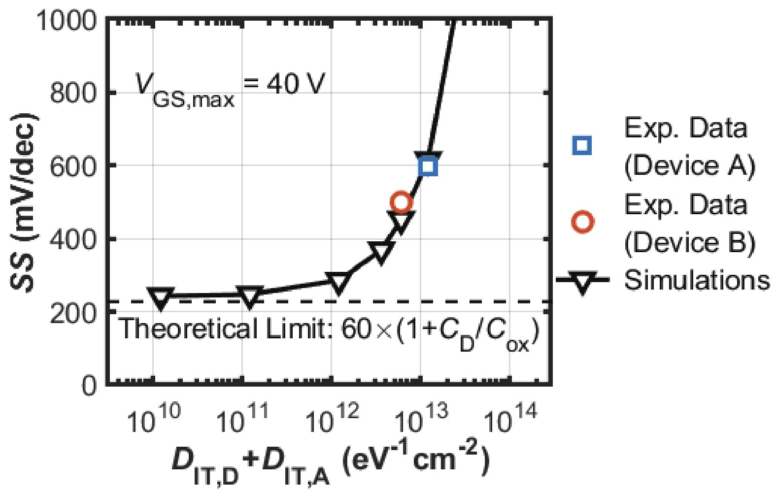
Table 1. Trap-related simulation parameters (Device A/Device B).
| Label* | Areal density (DIT, cm−2∙eV−1) | Volume density (DBT, cm−3∙eV−1) | Energy mean** (EM, eV) | Energy spread (ES, eV) |
| IT, A | 1 × 10¹³/5 × 1012 | // | 0 | 0.2 |
| IT, D | 2 × 10¹²/1 × 1012 | // | 0.9 | 1.6 |
| BT, A | // | 4 × 10¹⁹/1 × 1019 | 0 | 2 |
| *A stands for acceptors, D for donors. **With respect to GaN conduction band edge (EC). |
||||
 DownLoad: CSV
| [1] |
Fu H Q, Fu K, Chowdhury S, et al. Vertical GaN power devices: Device principles and fabrication technologies—Part II. IEEE Trans Electron Devices, 2021, 68, 3212 doi: 10.1109/TED.2021.3083209
|
| [2] |
Meneghini M, De Santi C, Abid I, et al. GaN-based power devices: Physics, reliability, and perspectives. J Appl Phys, 2021, 130, 181101 doi: 10.1063/5.0061354
|
| [3] |
del Alamo J A, Lee E S. Stability and reliability of lateral GaN power field-effect transistors. IEEE Trans Electron Devices, 2019, 66, 4578 doi: 10.1109/TED.2019.2931718
|
| [4] |
Zagni N, Chini A, Puglisi F M, et al. “hole redistribution” model explaining the thermally activated RON stress/recovery transients in carbon-doped AlGaN/GaN power MIS-HEMTs. IEEE Trans Electron Devices, 2021, 68, 697 doi: 10.1109/TED.2020.3045683
|
| [5] |
Cioni M, Zagni N, Iucolano F, et al. Partial recovery of dynamic RON versus OFF-state stress voltage in p-GaN gate AlGaN/GaN power HEMTs. IEEE Trans Electron Devices, 2021, 68, 4862 doi: 10.1109/TED.2021.3105075
|
| [6] |
Chini A, Meneghesso G, Meneghini M, et al. Experimental and numerical analysis of hole emission process from carbon-related traps in GaN buffer layers. IEEE Trans Electron Devices, 2016, 63, 3473 doi: 10.1109/TED.2016.2593791
|
| [7] |
Modolo N, De Santi C, Minetto A, et al. A physics-based approach to model hot-electron trapping kinetics in p-GaN HEMTs. IEEE Electron Device Lett, 2021, 42, 673 doi: 10.1109/LED.2021.3067796
|
| [8] |
Ohnishi K, Kawasaki S, Fujimoto N, et al. Vertical GaN p+-n junction diode with ideal avalanche capability grown by halide vapor phase epitaxy. Appl Phys Lett, 2021, 119, 152102 doi: 10.1063/5.0066139
|
| [9] |
Bian Z L, Zeng K, Chowdhury S. 2.8 kV avalanche in vertical GaN PN diode utilizing field plate on hydrogen passivated P-layer. IEEE Electron Device Lett, 2022, 43, 596 doi: 10.1109/LED.2022.3149748
|
| [10] |
Liu J, Xiao M, Zhang Y, et al. 1.2 kV vertical GaN fin JFETs with robust avalanche and fast switching capabilities. 2020 IEEE International Electron Devices Meeting (IEDM), San Francisco, CA, USA. IEEE, 2021, 23.2. 1 doi: 10.1109/IEDM13553.2020.9372048
|
| [11] |
Mukherjee K, De Santi C, Borga M, et al. Challenges and perspectives for vertical GaN-on-Si trench MOS reliability: From leakage current analysis to gate stack optimization. Materials, 2021, 14, 2316 doi: 10.3390/ma14092316
|
| [12] |
Treidel E B, Hilt O, Hoffmann V, et al. On the conduction properties of vertical GaN n-channel trench MISFETs. IEEE J Electron Devices Soc, 2021, 9, 215 doi: 10.1109/JEDS.2021.3056697
|
| [13] |
Mukherjee K, De Santi C, Borga M, et al. Use of bilayer gate insulator in GaN-on-Si vertical trench MOSFETs: Impact on performance and reliability. Materials, 2020, 13, 4740 doi: 10.3390/ma13214740
|
| [14] |
Dannecker K, Baringhaus J. Fully vertical gallium nitride trench MOSFETs fabricated with metal-free gate first process. J Vac Sci Technol B, 2021, 39, 032204 doi: 10.1116/6.0000980
|
| [15] |
Henn M, Huber C. Impact of gate dielectric deposition temperature on p-type inversion channel MOSFETs fabricated on GaN-on-Si. 2022 IEEE Workshop on Wide Bandgap Power Devices and Applications in Europe (WiPDA Europe), 2022, 1 doi: 10.1109/WiPDAEurope55971.2022.9936574
|
| [16] |
Pavan P, Zagni N, Puglisi F M, et al. The impact of interface and border traps on current–voltage, capacitance–voltage, and split-CV mobility measurements in InGaAs MOSFETs. Phys Status Solidi A, 2017, 214, 1600592 doi: 10.1002/pssa.201600592
|
| [17] |
Guo A, del Alamo J A. Unified mechanism for positive- and negative-bias temperature instability in GaN MOSFETs. IEEE Trans Electron Devices, 2017, 64, 2142 doi: 10.1109/TED.2017.2686840
|
| [18] |
Wu T L, Franco J, Marcon D, et al. Toward understanding positive bias temperature instability in fully recessed-gate GaN MISFETs. IEEE Trans Electron Devices, 2016, 63, 1853 doi: 10.1109/TED.2016.2539341
|
| [19] |
Lagger P, Reiner M, Pogany D, et al. Comprehensive study of the complex dynamics of forward bias-induced threshold voltage drifts in GaN based MIS-HEMTs by stress/recovery experiments. IEEE Trans Electron Devices, 2014, 61, 1022 doi: 10.1109/TED.2014.2303853
|
| [20] |
Fregolent M, Del Fiol A, De Santi C, et al. Threshold voltage instability in SiO2-gate semi-vertical GaN trench MOSFETs grown on silicon substrate. Microelectron Reliab, 2023, 150, 115130 doi: 10.1016/j.microrel.2023.115130
|
| [21] |
Synopsys. Sentaurus SDevice manual (S-2021.06), 2021
|
| [22] |
Schroder D K. Oxide and interface trapped charges, oxide thickness. John Wiley & Sons, Inc. , 2005, 319
|
| [23] |
Sze S M, Ng K K. Physics of semiconductor devices. John Wiley & Sons, Inc. , 2006
|
| [24] |
Yu M Z, McNab S, Al-Dhahir I, et al. Extracting band-tail interface state densities from measurements and modelling of space charge layer resistance. Sol Energy Mater Sol Cells, 2021, 231, 111307 doi: 10.1016/j.solmat.2021.111307
|
| [25] |
Selmi L, Caruso E, Carapezzi S, et al. Modelling nanoscale n-MOSFETs with III-V compound semiconductor channels: From advanced models for band structures, electrostatics and transport to TCAD. 2017 IEEE International Electron Devices Meeting (IEDM), 2018, 13.4. 1 doi: 10.1109/IEDM.2017.8268384
|


Article views: 1005 Times PDF downloads: 204 Times Cited by: 0 Times
Received: 22 July 2023 Revised: 19 October 2023 Online: Accepted Manuscript: 06 December 2023Uncorrected proof: 08 December 2023Published: 15 March 2024
| Citation: |
Nicolò Zagni, Manuel Fregolent, Andrea Del Fiol, Davide Favero, Francesco Bergamin, Giovanni Verzellesi, Carlo De Santi, Gaudenzio Meneghesso, Enrico Zanoni, Christian Huber, Matteo Meneghini, Paolo Pavan. Physical insights into trapping effects on vertical GaN-on-Si trench MOSFETs from TCAD[J]. Journal of Semiconductors, 2024, 45(3): 032501. doi: 10.1088/1674-4926/45/3/032501
N Zagni, M Fregolent, A D Fiol, D Favero, F Bergamin, G Verzellesi, C D Santi, G Meneghesso, E Zanoni, C Huber, M Meneghini, P Pavan. Physical insights into trapping effects on vertical GaN-on-Si trench MOSFETs from TCAD[J]. J. Semicond, 2024, 45(3): 032501. doi: 10.1088/1674-4926/45/3/032501
Export: BibTex EndNote

|
| [1] |
Fu H Q, Fu K, Chowdhury S, et al. Vertical GaN power devices: Device principles and fabrication technologies—Part II. IEEE Trans Electron Devices, 2021, 68, 3212 doi: 10.1109/TED.2021.3083209
|
| [2] |
Meneghini M, De Santi C, Abid I, et al. GaN-based power devices: Physics, reliability, and perspectives. J Appl Phys, 2021, 130, 181101 doi: 10.1063/5.0061354
|
| [3] |
del Alamo J A, Lee E S. Stability and reliability of lateral GaN power field-effect transistors. IEEE Trans Electron Devices, 2019, 66, 4578 doi: 10.1109/TED.2019.2931718
|
| [4] |
Zagni N, Chini A, Puglisi F M, et al. “hole redistribution” model explaining the thermally activated RON stress/recovery transients in carbon-doped AlGaN/GaN power MIS-HEMTs. IEEE Trans Electron Devices, 2021, 68, 697 doi: 10.1109/TED.2020.3045683
|
| [5] |
Cioni M, Zagni N, Iucolano F, et al. Partial recovery of dynamic RON versus OFF-state stress voltage in p-GaN gate AlGaN/GaN power HEMTs. IEEE Trans Electron Devices, 2021, 68, 4862 doi: 10.1109/TED.2021.3105075
|
| [6] |
Chini A, Meneghesso G, Meneghini M, et al. Experimental and numerical analysis of hole emission process from carbon-related traps in GaN buffer layers. IEEE Trans Electron Devices, 2016, 63, 3473 doi: 10.1109/TED.2016.2593791
|
| [7] |
Modolo N, De Santi C, Minetto A, et al. A physics-based approach to model hot-electron trapping kinetics in p-GaN HEMTs. IEEE Electron Device Lett, 2021, 42, 673 doi: 10.1109/LED.2021.3067796
|
| [8] |
Ohnishi K, Kawasaki S, Fujimoto N, et al. Vertical GaN p+-n junction diode with ideal avalanche capability grown by halide vapor phase epitaxy. Appl Phys Lett, 2021, 119, 152102 doi: 10.1063/5.0066139
|
| [9] |
Bian Z L, Zeng K, Chowdhury S. 2.8 kV avalanche in vertical GaN PN diode utilizing field plate on hydrogen passivated P-layer. IEEE Electron Device Lett, 2022, 43, 596 doi: 10.1109/LED.2022.3149748
|
| [10] |
Liu J, Xiao M, Zhang Y, et al. 1.2 kV vertical GaN fin JFETs with robust avalanche and fast switching capabilities. 2020 IEEE International Electron Devices Meeting (IEDM), San Francisco, CA, USA. IEEE, 2021, 23.2. 1 doi: 10.1109/IEDM13553.2020.9372048
|
| [11] |
Mukherjee K, De Santi C, Borga M, et al. Challenges and perspectives for vertical GaN-on-Si trench MOS reliability: From leakage current analysis to gate stack optimization. Materials, 2021, 14, 2316 doi: 10.3390/ma14092316
|
| [12] |
Treidel E B, Hilt O, Hoffmann V, et al. On the conduction properties of vertical GaN n-channel trench MISFETs. IEEE J Electron Devices Soc, 2021, 9, 215 doi: 10.1109/JEDS.2021.3056697
|
| [13] |
Mukherjee K, De Santi C, Borga M, et al. Use of bilayer gate insulator in GaN-on-Si vertical trench MOSFETs: Impact on performance and reliability. Materials, 2020, 13, 4740 doi: 10.3390/ma13214740
|
| [14] |
Dannecker K, Baringhaus J. Fully vertical gallium nitride trench MOSFETs fabricated with metal-free gate first process. J Vac Sci Technol B, 2021, 39, 032204 doi: 10.1116/6.0000980
|
| [15] |
Henn M, Huber C. Impact of gate dielectric deposition temperature on p-type inversion channel MOSFETs fabricated on GaN-on-Si. 2022 IEEE Workshop on Wide Bandgap Power Devices and Applications in Europe (WiPDA Europe), 2022, 1 doi: 10.1109/WiPDAEurope55971.2022.9936574
|
| [16] |
Pavan P, Zagni N, Puglisi F M, et al. The impact of interface and border traps on current–voltage, capacitance–voltage, and split-CV mobility measurements in InGaAs MOSFETs. Phys Status Solidi A, 2017, 214, 1600592 doi: 10.1002/pssa.201600592
|
| [17] |
Guo A, del Alamo J A. Unified mechanism for positive- and negative-bias temperature instability in GaN MOSFETs. IEEE Trans Electron Devices, 2017, 64, 2142 doi: 10.1109/TED.2017.2686840
|
| [18] |
Wu T L, Franco J, Marcon D, et al. Toward understanding positive bias temperature instability in fully recessed-gate GaN MISFETs. IEEE Trans Electron Devices, 2016, 63, 1853 doi: 10.1109/TED.2016.2539341
|
| [19] |
Lagger P, Reiner M, Pogany D, et al. Comprehensive study of the complex dynamics of forward bias-induced threshold voltage drifts in GaN based MIS-HEMTs by stress/recovery experiments. IEEE Trans Electron Devices, 2014, 61, 1022 doi: 10.1109/TED.2014.2303853
|
| [20] |
Fregolent M, Del Fiol A, De Santi C, et al. Threshold voltage instability in SiO2-gate semi-vertical GaN trench MOSFETs grown on silicon substrate. Microelectron Reliab, 2023, 150, 115130 doi: 10.1016/j.microrel.2023.115130
|
| [21] |
Synopsys. Sentaurus SDevice manual (S-2021.06), 2021
|
| [22] |
Schroder D K. Oxide and interface trapped charges, oxide thickness. John Wiley & Sons, Inc. , 2005, 319
|
| [23] |
Sze S M, Ng K K. Physics of semiconductor devices. John Wiley & Sons, Inc. , 2006
|
| [24] |
Yu M Z, McNab S, Al-Dhahir I, et al. Extracting band-tail interface state densities from measurements and modelling of space charge layer resistance. Sol Energy Mater Sol Cells, 2021, 231, 111307 doi: 10.1016/j.solmat.2021.111307
|
| [25] |
Selmi L, Caruso E, Carapezzi S, et al. Modelling nanoscale n-MOSFETs with III-V compound semiconductor channels: From advanced models for band structures, electrostatics and transport to TCAD. 2017 IEEE International Electron Devices Meeting (IEDM), 2018, 13.4. 1 doi: 10.1109/IEDM.2017.8268384
|

 WeChat ID
Journal of Semiconductors © 2017 All Rights Reserved 京ICP备05085259号-2


