


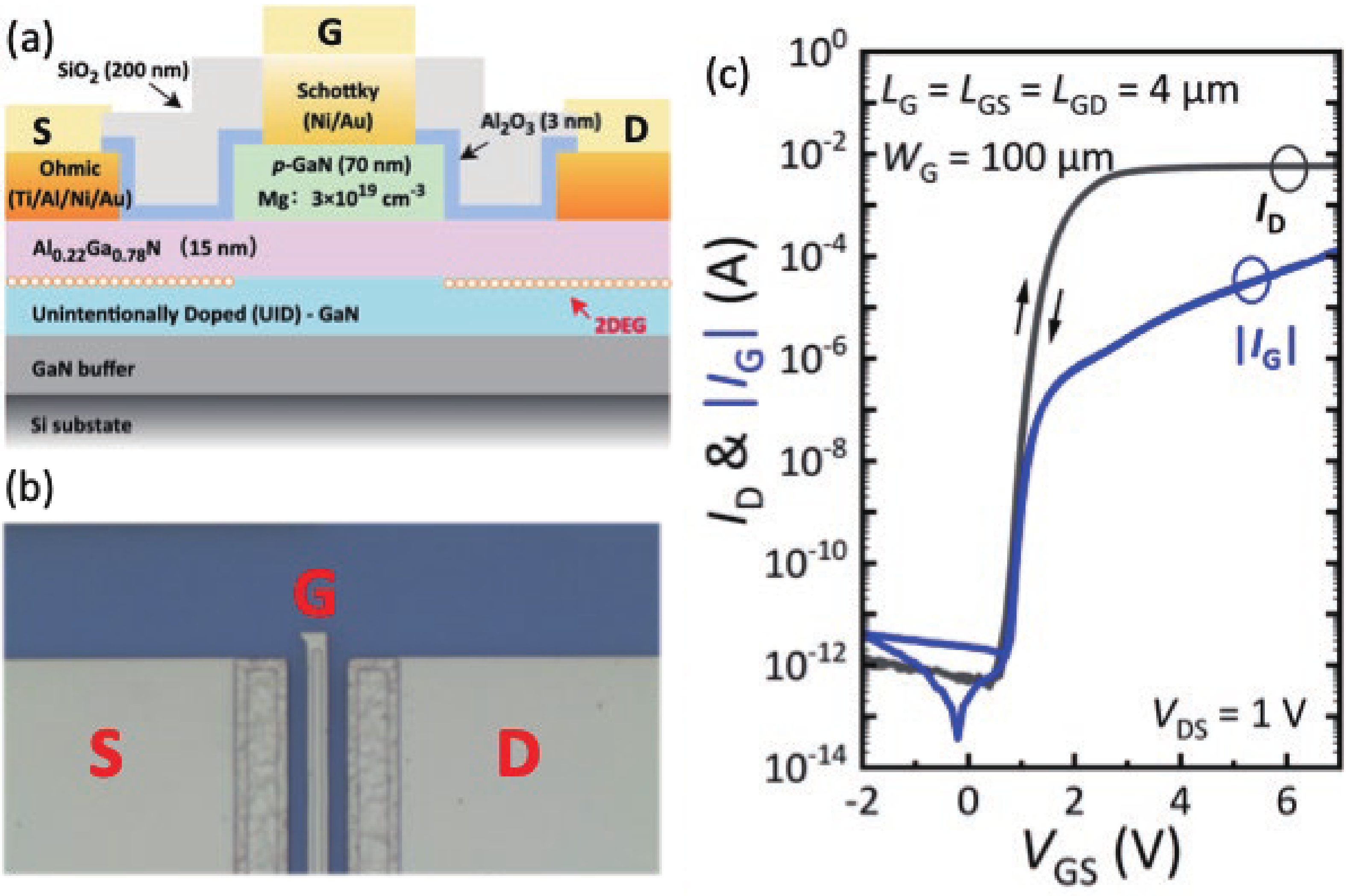
Fig. 1.
(Color online) Schematic diagram of the process flow of the Schottky-type p-GaN HEMT.
ARTICLES
Chao Feng1, 2, Xinyue Dai1, 2, Qimeng Jiang1, 2, , Sen Huang1, 2, , Jie Fan1, Xinhua Wang1, 2 and Xinyu Liu1, 2
Corresponding author: Qimeng Jiang, jiangqimeng@ime.ac.cn; Sen Huang, huangsen@ime.ac.cn
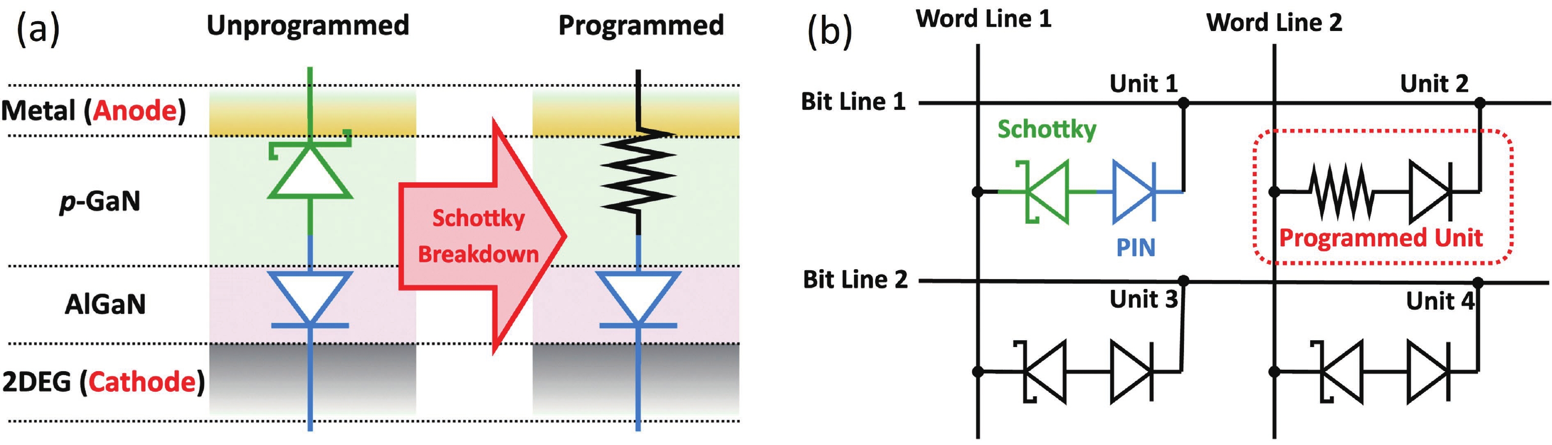
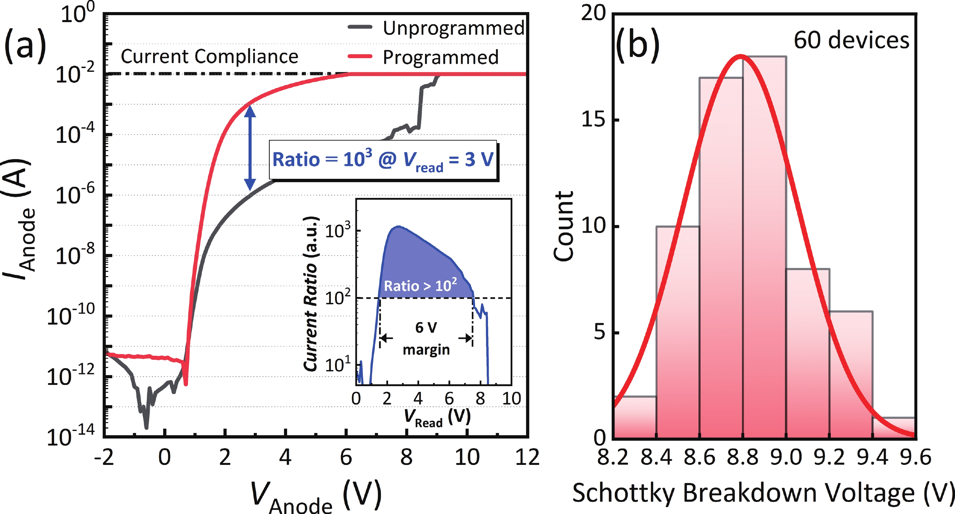
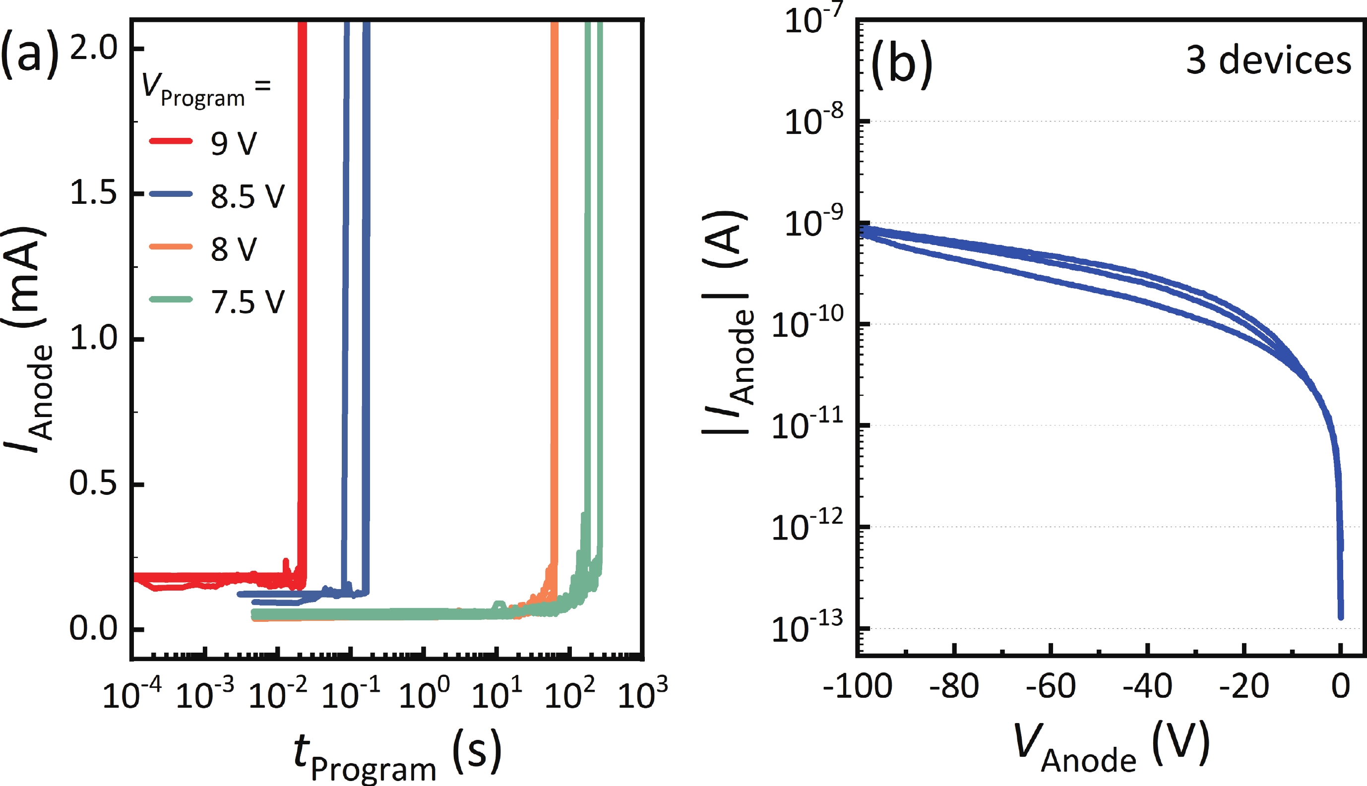
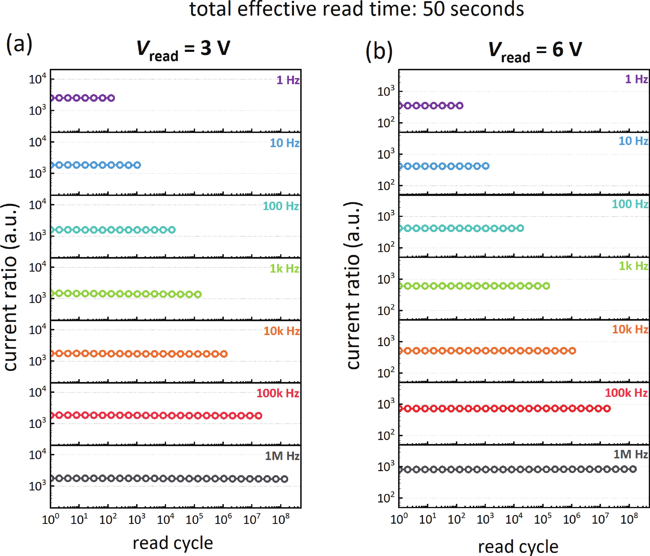
Abstract: In this work, a novel one-time-programmable memory unit based on a Schottky-type p-GaN diode is proposed. During the programming process, the junction switches from a high-resistance state to a low-resistance state through Schottky junction breakdown, and the state is permanently preserved. The memory unit features a current ratio of more than 103, a read voltage window of 6 V, a programming time of less than 10−4 s, a stability of more than 108 read cycles, and a lifetime of far more than 10 years. Besides, the fabrication of the device is fully compatible with commercial Si-based GaN process platforms, which is of great significance for the realization of low-cost read-only memory in all-GaN integration.
Key words: wide-bandgap semiconductor, one-time programmable, Schottky-type p-GaN diode, read-only memory device
| [1] |
Chen K J, Häberlen O, Lidow A, et al. GaN-on-Si power technology: Devices and applications. IEEE Trans Electron Devices, 2017, 64, 779 doi: 10.1109/TED.2017.2657579
|
| [2] |
Amano H, Baines Y, Borga M, et al. The 2018 GaN power electronics roadmap. J Phys D: Appl Phys. 51 163001 doi: 10.1088/1361-6463/aaaf9d
|
| [3] |
Zheng Z Y, Zhang L, Song W J, et al. Gallium nitride-based complementary logic integrated circuits. Nat Electron, 2021, 4, 595 doi: 10.1038/s41928-021-00611-y
|
| [4] |
Zheng Z, Xu H, Zhang L, et al. On the operating speed and energy efficiency of GaN-based monolithic complementary logic circuits for integrated power conversion systems. Fundamental Research, 2021 , 1, 661 doi: 10.1016/j.fmre.2021.09.015
|
| [5] |
Chen Y R, Song H, Jiang H, et al. Reproducible bipolar resistive switching in entire nitride AlN/n-GaN metal-insulator-semiconductor device and its mechanism. Appl Phys Lett, 2014, 105, 193502 doi: 10.1063/1.4901747
|
| [6] |
Chen T, Zheng Z Y, Feng S R, et al. Endurance improvement of GaN bipolar charge trapping memory with back gate injection. IEEE Electron Device Lett, 2023, 44, 1408 doi: 10.1109/LED.2023.3299961
|
| [7] |
Fu K, Fu H Q, Huang X Q, et al. Threshold switching and memory behaviors of epitaxially regrown GaN-on-GaN vertical p-n diodes with high temperature stability. IEEE Electron Device Lett, 2019, 40, 375 doi: 10.1109/LED.2019.2891391
|
| [8] |
Yuan M Y, Xie Q Y, Niroula J, et al. GaN memory operational at 300 °C. IEEE Electron Device Lett, 2022, 43, 2053 doi: 10.1109/LED.2022.3218671
|
| [9] |
Sayadi L, Iannaccone G, Sicre S, et al. Threshold voltage instability in p-GaN gate AlGaN/GaN HFETs. IEEE Trans Electron Devices, 2018, 65, 2454 doi: 10.1109/TED.2018.2828702
|
| [10] |
He J, Chan W T, Wang C, et al. A compact CMOS compatible oxide antifuse with polysilicon diode driver. IEEE Trans Electron Devices, 2012, 59, 2539 doi: 10.1109/TED.2012.2201941
|
| [11] |
Kuo R J, Chang F C, King Y C, et al. Antifuse OTP cell in a cross-point array by advanced CMOS FinFET process. IEEE Trans Electron Devices, 2019, 66, 1729 doi: 10.1109/TED.2019.2900282
|
| [12] |
Ng K P, Lee M C, Kwong K C, et al. Diode based gate oxide anti-fuse one time programmable memory array in standard CMOS process. 2009 IEEE International Conference of Electron Devices and Solid-State Circuits (EDSSC), 2010, 457 doi: 10.1109/EDSSC.2009.5394219
|
| [13] |
Pushpakaran B N, Subburaj A S, Bayne S B. Commercial GaN-based power electronic systems: A review. J Electron Mater, 2020, 49, 6247 doi: 10.1007/s11664-020-08397-z
|
| [14] |
Dai X Y, Ji Z C, Jiang Q M, et al. Suppression of reverse leakage in enhancement-mode GaN high-electron-mobility transistor by extended PGaN technology. Phys Status Solidi A, 2023, 220, 2200692 doi: 10.1002/pssa.202200692
|
| [15] |
Tallarico A N, Stoffels S, Magnone P, et al. Investigation of the p-GaN gate breakdown in forward-biased GaN-based power HEMTs. IEEE Electron Device Lett, 2017, 38, 99 doi: 10.1109/LED.2016.2631640
|
| [16] |
Feng C, Jiang Q M, Huang S, et al. Gate-bias-accelerated VTH recovery on schottky-type p-GaN gate AlGaN/GaN HEMTs. IEEE Trans Electron Devices, 2023, 70, 4591 doi: 10.1109/TED.2023.3297568
|
| [17] |
Lee F, Su L Y, Wang C H, et al. Impact of gate metal on the performance of p-GaN/AlGaN/GaN high electron mobility transistors. IEEE Electron Device Lett, 2015, 36, 232 doi: 10.1109/LED.2015.2395454
|
| [18] |
Wu T L, Marcon D, You S Z, et al. Forward bias gate breakdown mechanism in enhancement-mode p-GaN gate AlGaN/GaN high-electron mobility transistors. IEEE Electron Device Lett, 2015, 36, 1001 doi: 10.1109/LED.2015.2465137
|
| [19] |
Stoffels S, Bakeroot B, Wu T L, et al. Failure mode for p-GaN gates under forward gate stress with varying Mg concentration. 2017 IEEE International Reliability Physics Symposium (IRPS), 2017, 4B doi: 10.1109/IRPS.2017.7936310
|
| [20] |
Masin F, Meneghini M, Canato E, et al. Positive temperature dependence of time-dependent breakdown of GaN-on-Si E-mode HEMTs under positive gate stress. Appl Phys Lett, 2019, 115, 052103 doi: 10.1063/1.5109301
|


Article views: 322 Times PDF downloads: 56 Times Cited by: 0 Times
Received: 21 October 2023 Revised: 09 November 2023 Online: Accepted Manuscript: 11 December 2023Uncorrected proof: 13 December 2023Published: 15 March 2024
| Citation: |
Chao Feng, Xinyue Dai, Qimeng Jiang, Sen Huang, Jie Fan, Xinhua Wang, Xinyu Liu. A novel one-time-programmable memory unit based on Schottky-type p-GaN diode[J]. Journal of Semiconductors, 2024, 45(3): 032502. doi: 10.1088/1674-4926/45/3/032502
C Feng, X Y Dai, Q M Jiang, S Huang, J Fan, X H Wang, X Y Liu. A novel one-time-programmable memory unit based on Schottky-type p-GaN diode[J]. J. Semicond, 2024, 45(3): 032502. doi: 10.1088/1674-4926/45/3/032502
Export: BibTex EndNote

|
| [1] |
Chen K J, Häberlen O, Lidow A, et al. GaN-on-Si power technology: Devices and applications. IEEE Trans Electron Devices, 2017, 64, 779 doi: 10.1109/TED.2017.2657579
|
| [2] |
Amano H, Baines Y, Borga M, et al. The 2018 GaN power electronics roadmap. J Phys D: Appl Phys. 51 163001 doi: 10.1088/1361-6463/aaaf9d
|
| [3] |
Zheng Z Y, Zhang L, Song W J, et al. Gallium nitride-based complementary logic integrated circuits. Nat Electron, 2021, 4, 595 doi: 10.1038/s41928-021-00611-y
|
| [4] |
Zheng Z, Xu H, Zhang L, et al. On the operating speed and energy efficiency of GaN-based monolithic complementary logic circuits for integrated power conversion systems. Fundamental Research, 2021 , 1, 661 doi: 10.1016/j.fmre.2021.09.015
|
| [5] |
Chen Y R, Song H, Jiang H, et al. Reproducible bipolar resistive switching in entire nitride AlN/n-GaN metal-insulator-semiconductor device and its mechanism. Appl Phys Lett, 2014, 105, 193502 doi: 10.1063/1.4901747
|
| [6] |
Chen T, Zheng Z Y, Feng S R, et al. Endurance improvement of GaN bipolar charge trapping memory with back gate injection. IEEE Electron Device Lett, 2023, 44, 1408 doi: 10.1109/LED.2023.3299961
|
| [7] |
Fu K, Fu H Q, Huang X Q, et al. Threshold switching and memory behaviors of epitaxially regrown GaN-on-GaN vertical p-n diodes with high temperature stability. IEEE Electron Device Lett, 2019, 40, 375 doi: 10.1109/LED.2019.2891391
|
| [8] |
Yuan M Y, Xie Q Y, Niroula J, et al. GaN memory operational at 300 °C. IEEE Electron Device Lett, 2022, 43, 2053 doi: 10.1109/LED.2022.3218671
|
| [9] |
Sayadi L, Iannaccone G, Sicre S, et al. Threshold voltage instability in p-GaN gate AlGaN/GaN HFETs. IEEE Trans Electron Devices, 2018, 65, 2454 doi: 10.1109/TED.2018.2828702
|
| [10] |
He J, Chan W T, Wang C, et al. A compact CMOS compatible oxide antifuse with polysilicon diode driver. IEEE Trans Electron Devices, 2012, 59, 2539 doi: 10.1109/TED.2012.2201941
|
| [11] |
Kuo R J, Chang F C, King Y C, et al. Antifuse OTP cell in a cross-point array by advanced CMOS FinFET process. IEEE Trans Electron Devices, 2019, 66, 1729 doi: 10.1109/TED.2019.2900282
|
| [12] |
Ng K P, Lee M C, Kwong K C, et al. Diode based gate oxide anti-fuse one time programmable memory array in standard CMOS process. 2009 IEEE International Conference of Electron Devices and Solid-State Circuits (EDSSC), 2010, 457 doi: 10.1109/EDSSC.2009.5394219
|
| [13] |
Pushpakaran B N, Subburaj A S, Bayne S B. Commercial GaN-based power electronic systems: A review. J Electron Mater, 2020, 49, 6247 doi: 10.1007/s11664-020-08397-z
|
| [14] |
Dai X Y, Ji Z C, Jiang Q M, et al. Suppression of reverse leakage in enhancement-mode GaN high-electron-mobility transistor by extended PGaN technology. Phys Status Solidi A, 2023, 220, 2200692 doi: 10.1002/pssa.202200692
|
| [15] |
Tallarico A N, Stoffels S, Magnone P, et al. Investigation of the p-GaN gate breakdown in forward-biased GaN-based power HEMTs. IEEE Electron Device Lett, 2017, 38, 99 doi: 10.1109/LED.2016.2631640
|
| [16] |
Feng C, Jiang Q M, Huang S, et al. Gate-bias-accelerated VTH recovery on schottky-type p-GaN gate AlGaN/GaN HEMTs. IEEE Trans Electron Devices, 2023, 70, 4591 doi: 10.1109/TED.2023.3297568
|
| [17] |
Lee F, Su L Y, Wang C H, et al. Impact of gate metal on the performance of p-GaN/AlGaN/GaN high electron mobility transistors. IEEE Electron Device Lett, 2015, 36, 232 doi: 10.1109/LED.2015.2395454
|
| [18] |
Wu T L, Marcon D, You S Z, et al. Forward bias gate breakdown mechanism in enhancement-mode p-GaN gate AlGaN/GaN high-electron mobility transistors. IEEE Electron Device Lett, 2015, 36, 1001 doi: 10.1109/LED.2015.2465137
|
| [19] |
Stoffels S, Bakeroot B, Wu T L, et al. Failure mode for p-GaN gates under forward gate stress with varying Mg concentration. 2017 IEEE International Reliability Physics Symposium (IRPS), 2017, 4B doi: 10.1109/IRPS.2017.7936310
|
| [20] |
Masin F, Meneghini M, Canato E, et al. Positive temperature dependence of time-dependent breakdown of GaN-on-Si E-mode HEMTs under positive gate stress. Appl Phys Lett, 2019, 115, 052103 doi: 10.1063/1.5109301
|

 WeChat ID
Journal of Semiconductors © 2017 All Rights Reserved 京ICP备05085259号-2

 DownLoad:

