


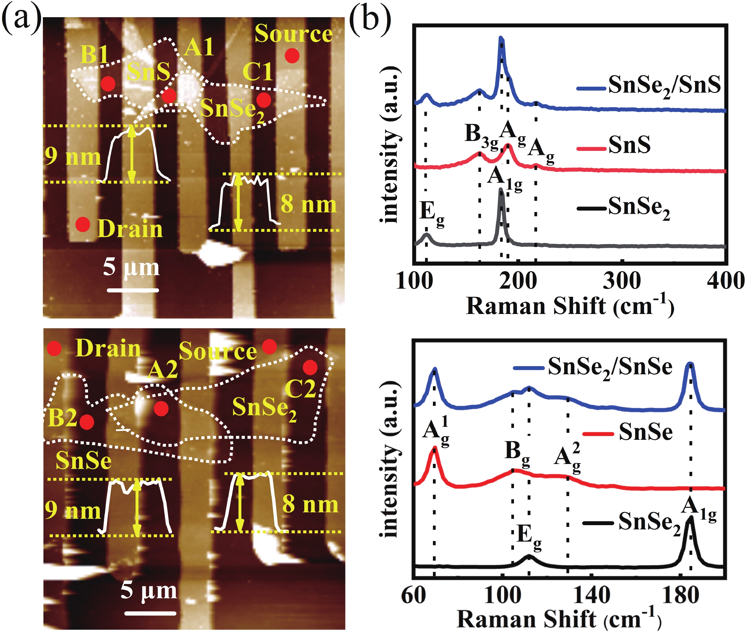
Fig. 1.
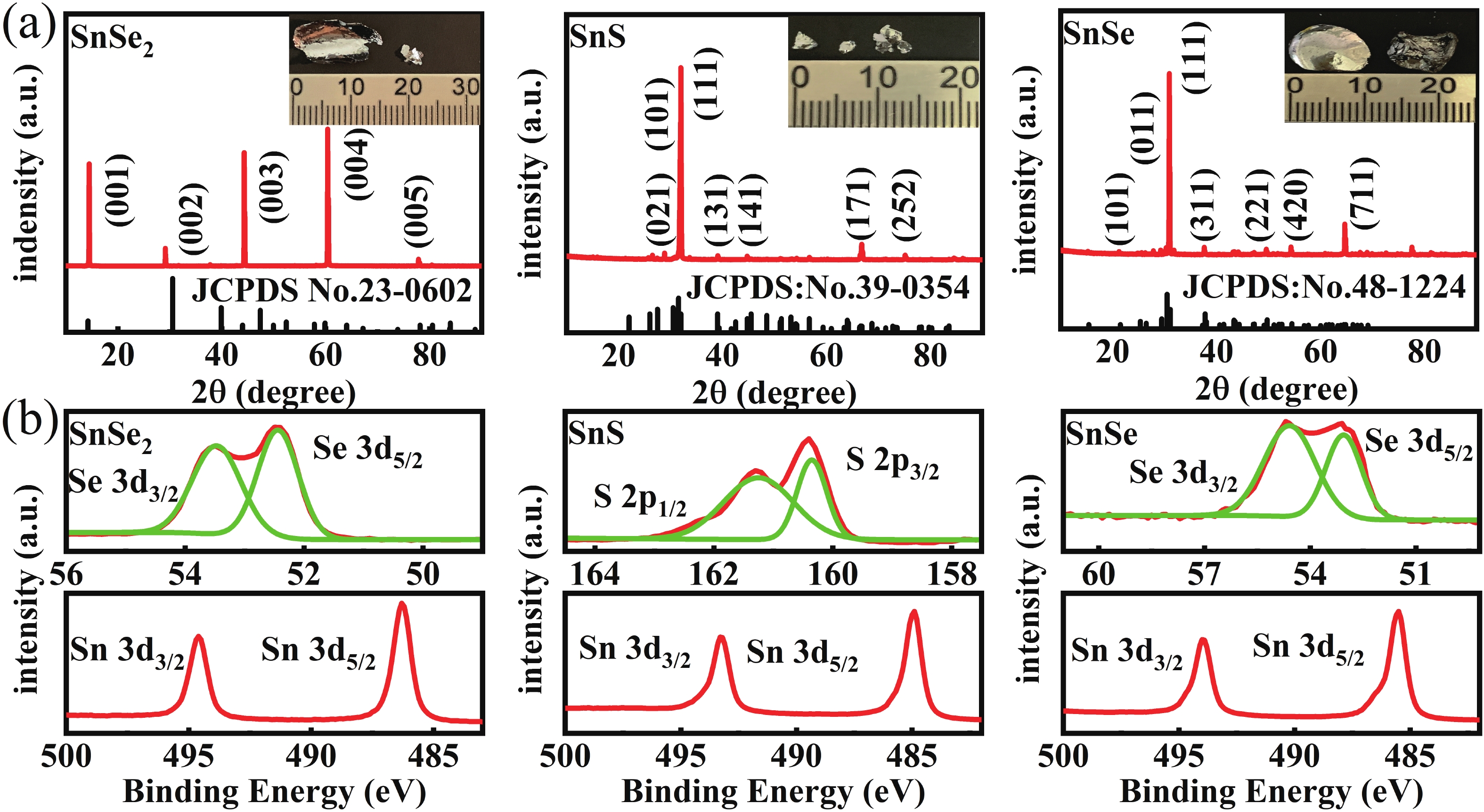
(Color online) (a) XRD patterns of the SnSe2, SnS, and SnSe crystals. The insets are the corresponding optical microscopy images. (b) XPS spectra of the SnS, SnS, and SnSe crystals.
ARTICLES
Xinfa Zhu1, §, Weishuai Duan1, §, Xiancheng Meng1, Xiyu Jia1, Yonghui Zhang1, Pengyu Zhou2, , Mengjun Wang1, Hongxing Zheng1 and Chao Fan1,
Corresponding author: Pengyu Zhou, 20162715@neepu.edu.cn; Chao Fan, fanch@hebut.edu.cn
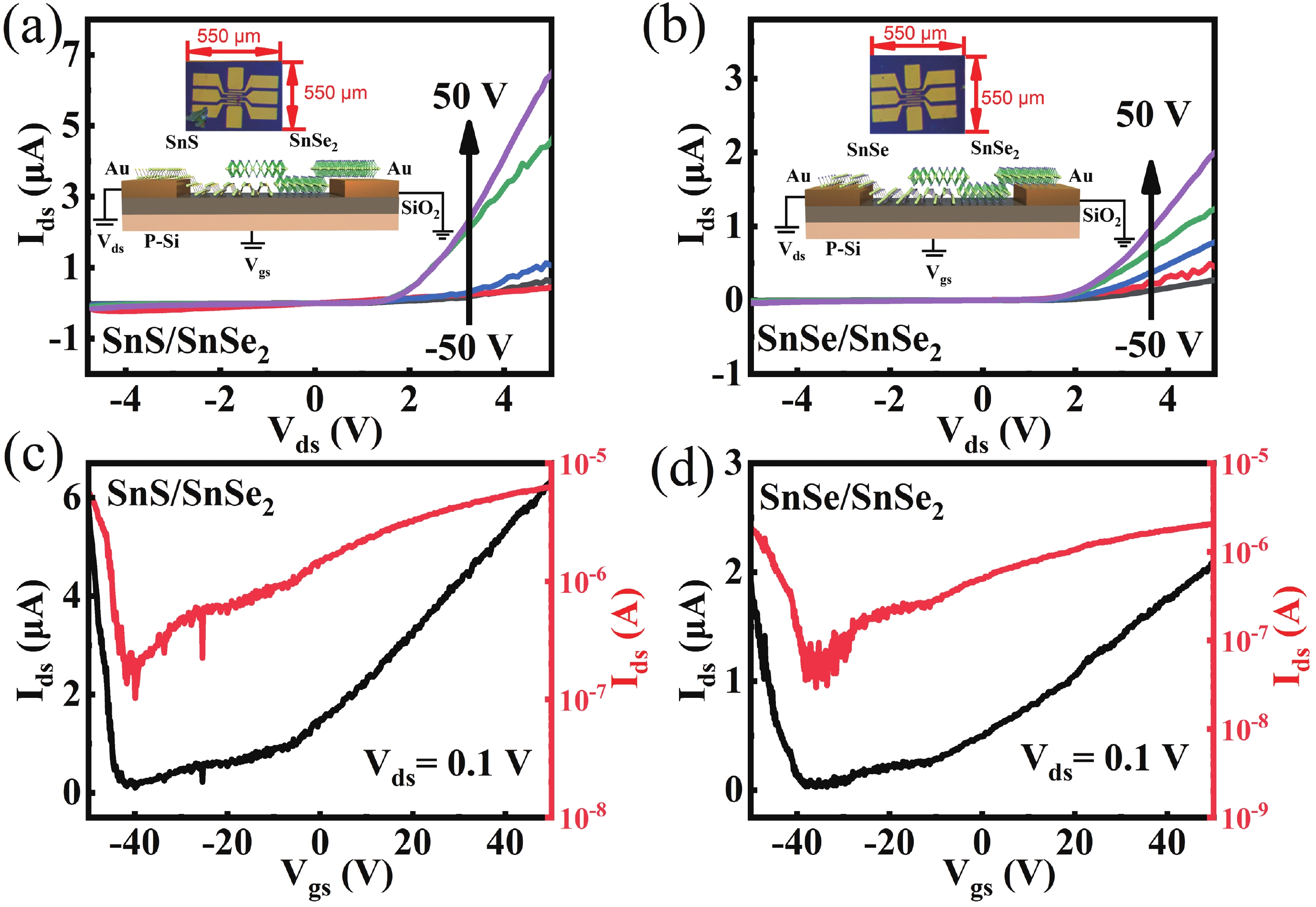
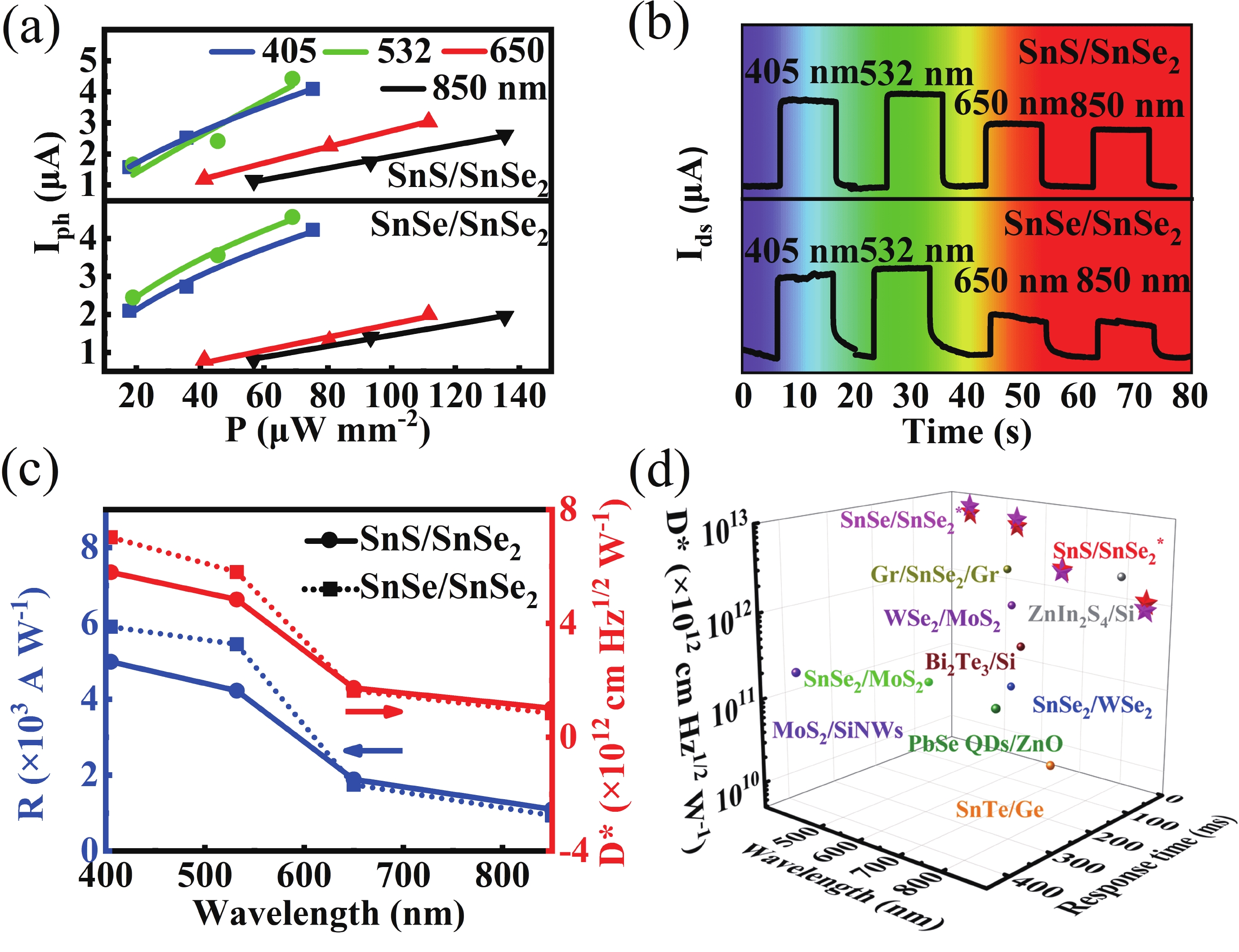
Abstract: The emergent two-dimensional (2D) material, tin diselenide (SnSe2), has garnered significant consideration for its potential in image capturing systems, optical communication, and optoelectronic memory. Nevertheless, SnSe2-based photodetection faces obstacles, including slow response speed and low normalized detectivity. In this work, photodetectors based on SnS/SnSe2 and SnSe/SnSe2 p−n heterostructures have been implemented through a polydimethylsiloxane (PDMS)−assisted transfer method. These photodetectors demonstrate broad-spectrum photoresponse within the 405 to 850 nm wavelength range. The photodetector based on the SnS/SnSe2 heterostructure exhibits a significant responsivity of 4.99 × 10³ A∙W−1, normalized detectivity of 5.80 × 1012 cm∙Hz1/2∙W−1, and fast response time of 3.13 ms, respectively, owing to the built-in electric field. Meanwhile, the highest values of responsivity, normalized detectivity, and response time for the photodetector based on the SnSe/SnSe2 heterostructure are 5.91 × 10³ A∙W−1, 7.03 × 1012 cm∙Hz1/2∙W−1, and 4.74 ms, respectively. And their photodetection performances transcend those of photodetectors based on individual SnSe2, SnS, SnSe, and other commonly used 2D materials. Our work has demonstrated an effective strategy to improve the performance of SnSe2-based photodetectors and paves the way for their future commercialization.
Key words: two-dimensional materials, tin diselenide, heterostructures, broad-spectrum photodetectors
| [1] |
Novoselov K S, Geim A K, Morozov S V, et al. Electric field effect in atomically thin carbon films. Science, 2004, 306, 666 doi: 10.1126/science.1102896
|
| [2] |
Lien M R, Wang N, Wu J, et al. Resonant grating-enhanced black phosphorus mid-wave infrared photodetector. Nano Lett, 2022, 22(21), 8704 doi: 10.1021/acs.nanolett.2c03469
|
| [3] |
Zhang F, Mo Z X, Cui B C, et al. Bandgap engineering of BiIns nanowire for wide-spectrum, high-responsivity, and polarimetric-sensitive detection. Adv Funct Material, 2023, 2306077
|
| [4] |
Rahman A, Kim H, Noor-A-Alam M, et al. A theoretical study on tuning band gaps of monolayer and bilayer SnS2 and SnSe2 under external stimuli. Curr Appl Phys, 2019, 19(31), 709
|
| [5] |
Shafique A, Samad A, Shin Y H. Ultra low lattice thermal conductivity and high carrier mobility of monolayer SnS2 and SnSe2: A first principles study. Phys Chem Chem Phys, 2017, 19, 20677 doi: 10.1039/C7CP03748A
|
| [6] |
Bibin J, Kunjomana A G, Teena M. Physical vapor deposition and enhancement of optoelectronic properties of SnSe2 platelets. Sci Mater Electron, 2022, 33(35), 26397 doi: 10.1007/s10854-022-09320-4
|
| [7] |
Mukhokosi E P, Roul B, Krupanidhi S B, et al. Toward a fast and highly responsive SnSe2-based photodiode by exploiting the mobility of the counter semiconductor. ACS Appl Mater Interfaces, 2019, 11(6), 6184 doi: 10.1021/acsami.8b16635
|
| [8] |
Dong W, Lu C H, Luo M W, et al. Enhanced UV−Vis photodetector performance by optimizing interfacial charge transportation in the heterostructure by SnS and SnSe2. J Colloid Interface Sci, 2022, 621, 374 doi: 10.1016/j.jcis.2022.04.041
|
| [9] |
Guo C, Guo W L, Xu H A, et al. Ultrasensitive ambient-stable SnSe2-based broadband photodetectors for room-temperature IR/THz energy conversion and imaging. 2D Mater, 2020, 7(3), 035026 doi: 10.1088/2053-1583/ab8ec0
|
| [10] |
Lv S, Liu X, Li X, et al. Electrochemical peeling few-layer SnSe2 for high-performance ultrafast photonics. ACS Appl Mater Interfaces, 2020, 12(38), 43049 doi: 10.1021/acsami.0c10079
|
| [11] |
Wang R Y, Caldwell M A, Jeyasingh R G D, et al. Electronic and optical switching of solution−phase deposited SnSe2 phase change memory material. J Appl Phys, 2011, 109(11), 113506 doi: 10.1063/1.3587187
|
| [12] |
Chen Z, Xiong L, Li G, et al. Wafer-scale growth of vertical-structured SnSe2 nanosheets for highly sensitive, fast-response UV−vis−NIR broadband photodetectors. Adv Opt Mater, 2022, 10(5), 2102250 doi: 10.1002/adom.202102250
|
| [13] |
Zhou X, Gan L, Tian W, et al. Ultrathin SnSe2 flakes grown by chemical vapor deposition for high-performance photodetectors. Adv Mater, 2015, 27(48), 8035 doi: 10.1002/adma.201503873
|
| [14] |
Park H, Shin G H, Lee K J, et al. Probing temperature-dependent interlayer coupling in a MoS2/h-BN heterostructure. Nano Res, 2020, 13(2), 576 doi: 10.1007/s12274-020-2658-3
|
| [15] |
Guo T T, Song X F, Wei P F, et al. High-gain MoS2/Ta2NiSe5 heterojunction photodetectors with charge transfer and suppressing dark current. ACS Appl Mater Interfaces, 2022, 14(50), 56384 doi: 10.1021/acsami.2c17495
|
| [16] |
Zhou X, Zhou N, Li C, et al. Vertical heterostructures based on SnSe2/MoS2 for high performance photodetectors. 2D Mater, 2017, 4(2), 025048 doi: 10.1088/2053-1583/aa6422
|
| [17] |
Zheng Z Q, Chen P F, Lu J T, et al. Self-assembly In2Se3/SnSe2 heterostructure array with suppressed dark current and enhanced photosensitivity for weak signal. Sci China Mater, 2020, 63(8), 1560 doi: 10.1007/s40843-020-1354-2
|
| [18] |
Kawamoto H, Higashitarumizu N, Nagamura N, et al. Micrometer-scale monolayer SnS growth by physical vapor deposition. Nanoscale, 2020, 12(45), 23274 doi: 10.1039/D0NR06022D
|
| [19] |
Zhao S L, Wang H, Zhou Y, et al. Controlled synthesis of single-crystal SnSe nanoplates. Nano Res, 2015, 8(1), 288 doi: 10.1007/s12274-014-0676-8
|
| [20] |
Arokiya Mary T, Fernandez A C, Sakthivel P, et al. A study on the role of surfactant on the layered growth of SnSe2 for electrical applications. J Mater Sci Mater Electron, 2016, 27(10), 11041 doi: 10.1007/s10854-016-5220-z
|
| [21] |
Lu C L, Zhang Y W, Zhang L, et al. Preparation and photoelectrochemical properties of SnS/SnSe and SnSe/SnS bilayer structures fabricated via electrodeposition. Appl Surf Sci, 2019, 484, 560 doi: 10.1016/j.apsusc.2019.04.104
|
| [22] |
Cho S H, Cho K, Park N W, et al. Multi-layer SnSe nanoflake field-effect transistors with low-resistance Au ohmic contacts. Nanoscale Res Lett, 2017, 12(1), 373 doi: 10.1186/s11671-017-2145-2
|
| [23] |
Kees de Groot C H, Gurnani C, Hector A L, et al. Highly selective chemical vapor deposition of tin diselenide thin films onto patterned substrates via single source diselenoether precursors. Chem Mater, 2012, 24(22), 4442 doi: 10.1021/cm302864x
|
| [24] |
Kumar M, Patel M, Kim J, et al. Vertically aligned crystalline SnS layers-based NIR photodetector governed by pyro-phototronic effect. Mater Lett, 2018, 213, 122 doi: 10.1016/j.matlet.2017.11.030
|
| [25] |
Saini S, Mele P, Tiwari A. Influence of the planar orientation of the substrate on thermoelectric response of SnSe thin films. J Phys Chem Solids, 2019, 129, 347 doi: 10.1016/j.jpcs.2019.01.010
|
| [26] |
Li C, Yan X A, Song X F, et al. WSe2/MoS2 and MoTe2/SnSe2 van der Waals heterostructure transistors with different band alignment. Nanotechnology, 2017, 28(41), 415201 doi: 10.1088/1361-6528/aa810f
|
| [27] |
Sohila S, Rajalakshmi M, Ghosh C, et al. Optical and Raman scattering studies on SnS nanoparticles. J Alloy Compd, 2011, 509(19), 5843 doi: 10.1016/j.jallcom.2011.02.141
|
| [28] |
Lee Y, Um D S, Lim S, et al. Gate-tunable and programmable n-InGaAs/Black phosphorus heterojunction diodes. ACS Appl Mater Interfaces, 2019, 11(26), 23382 doi: 10.1021/acsami.9b07701
|
| [29] |
Yao J D, Shao J M, Wang Y X, et al. Ultra-broadband and high response of the Bi2Te3−Si heterojunction and its application as a photodetector at room temperature in harsh working environments. Nanoscale, 2015, 29(7), 12535
|
| [30] |
Tian X Y, Liu Y S. Van der waals heterojunction ReSe2/WSe2 polarization-resolved photodetector. J Semicond, 2021, 42(3), 032001 doi: 10.1088/1674-4926/42/3/032001
|
| [31] |
Wang Y F, Li X Z, Liu P, et al. Epitaxial growth of CsPbBr3/PbS single-crystal film heterostructures for photodetection. J Semicond, 2021, 42(11), 112001 doi: 10.1088/1674-4926/42/11/112001
|
| [32] |
Zhu W K, Wei X, Yan F G, et al. Broadband polarized photodetector based on p-BP/n-ReS2 heterojunction. J Semicond, 2019, 40(9), 092001 doi: 10.1088/1674-4926/40/9/092001
|
| [33] |
Wang F, Zhang T, Xie R Z, et al. How to characterize figures of merit of two-dimensional photodetectors. Nat Commun, 2023, 14, 2224 doi: 10.1038/s41467-023-37635-1
|
| [34] |
Gong X, Tong M H, Xia Y J, et al. High-detectivity polymer photodetectors with spectral response from 300 nm to 1450 nm. Science, 2009, 325, 1665 doi: 10.1126/science.1176706
|
| [35] |
Wang W, Zhao D, Zhang F, et al. Highly sensitive low-bandgap perovskite photodetectors with response from ultraviolet to the near-infrared region. Adv Funct Mater, 2017, 27(42), 1703953 doi: 10.1002/adfm.201703953
|
| [36] |
Kublitski J, Hofacker A, Boroujeni B K, et al. Reverse dark current in organic photodetectors and the major role of traps as source of noise. Nat Commun, 2021, 12, 551 doi: 10.1038/s41467-020-20856-z
|
| [37] |
Pedapudi M C, Dhar J C. Ultrasensitive p-n junction UV-C photodetector based on p-Si/β-Ga2O3 nanowire arrays. Sens Actuat A, 2022, 344, 113673 doi: 10.1016/j.sna.2022.113673
|
| [38] |
Shin G H, Park C, Lee K J, et al. Ultrasensitive phototransistor based on WSe2-MoS2 van der waals heterojunction. Nano Lett, 2020, 20(8), 5741 doi: 10.1021/acs.nanolett.0c01460
|
| [39] |
Song L Y, Tang L B, Hao Q, et al. Broadband photodetector based on SnTe nanofilm/n-Ge heterostructure. Nanotechnology, 2022, 33(42), 425203 doi: 10.1088/1361-6528/ac80cc
|
| [40] |
Xue H, Dai Y, Kim W, et al. High photoresponsivity and broadband photodetection with a band-engineered WSe2/SnSe2 heterostructure. Nanoscale, 2019, 11(7), 3240 doi: 10.1039/C8NR09248F
|
| [41] |
Peng M F, Tao Y, Hong X K, et al. One-step synthesized PbSe nanocrystal inks decorated 2D MoS2 heterostructure for high stability photodetectors with photoresponse extending to near-infrared region. J Mater Chem C, 2022, 10(6), 2236 doi: 10.1039/D1TC05837A
|
| [42] |
Gao W, Zheng Z Q, Li Y T, et al. High performance tin diselenide photodetectors dependent on thickness: A vertical graphene sandwiched device and interfacial mechanism. Nanoscale, 2019, 11(28), 13309 doi: 10.1039/C9NR01966A
|
| [43] |
Peng M F, Liu Y, Li F, et al. Room-temperature direct synthesis of PbSe quantum dot inks for high-detectivity near-infrared photodetectors. ACS Appl Mater Interfaces, 2021, 13(43), 51198 doi: 10.1021/acsami.1c13723
|
| [44] |
Zheng Z Q, Yao J D, Li W J, et al. Fabrication of a high performance ZnIn2S4/Si heterostructure photodetector array for weak signal detection. J Mater Chem C, 2018, 6(47), 12928 doi: 10.1039/C8TC04692A
|
| [45] |
Yao J D, Shao J M, Wang Y X, et al. Ultra-broadband and high response of the Bi2Te3−Si heterojunction and its application as a photodetector at room temperature in harsh working environments. Nanoscale, 2015, 7, 12535 doi: 10.1039/C5NR02953H
|
| [46] |
Sharmila B, Dwivedi P. MoS2/SiNWs heterostructure based repeatable and highly responsive photodetector. Opt Mater, 2022, 133, 112918 doi: 10.1016/j.optmat.2022.112918
|
| [47] |
Xu Z H, Tang L, Zhang S W, et al. 2D MoS2/CuPc heterojunction based highly sensitive photodetectors through ultrafast charge transfer. Mater Today Phys, 2020, 15, 100273 doi: 10.1016/j.mtphys.2020.100273
|
| [48] |
Loos P F. Exchange functionals based on finite uniform electron gases. J Chem Phys, 2017, 146(11), 114108 doi: 10.1063/1.4978409
|
| [49] |
Yuan L, Xu Z J, Li J C, et al. Broad-spectrum and ultrasensitive photodetectors based on GeSe/SnS2 heterostructures with type-III band alignment. Appl Phys Lett, 2023, 122(24), 241106 doi: 10.1063/5.0154429
|
| [50] |
Li K Z, Zhu Y E, Zhang Y F, et al. Built-in electric field promotes photoexcitation separation and depletion of most carriers in TiO2: C UV detectors. Nanotechnology, 2019, 30(29), 295502 doi: 10.1088/1361-6528/ab15f0
|
| [51] |
Varghese A, Saha D, Thakar K, et al. Near-direct bandgap WSe2/ReS2 type−II pn heterojunction for enhanced ultrafast photodetection and high-performance photovoltaics. Nano Lett, 2020, 20(3), 1707 doi: 10.1021/acs.nanolett.9b04879
|
| [52] |
Nguyen T T, Patel M, Ban D K, et al. Vertically trigonal WS2 layer embedded heterostructure for enhanced ultraviolet−visible photodetector. J Alloy Compd, 2018, 768, 143 doi: 10.1016/j.jallcom.2018.07.164
|


Article views: 392 Times PDF downloads: 71 Times Cited by: 0 Times
Received: 07 November 2023 Revised: 22 November 2023 Online: Accepted Manuscript: 26 December 2023Uncorrected proof: 26 December 2023Published: 15 March 2024
| Citation: |
Xinfa Zhu, Weishuai Duan, Xiancheng Meng, Xiyu Jia, Yonghui Zhang, Pengyu Zhou, Mengjun Wang, Hongxing Zheng, Chao Fan. Visible-to-near-infrared photodetectors based on SnS/SnSe2 and SnSe/SnSe2 p−n heterostructures with a fast response speed and high normalized detectivity[J]. Journal of Semiconductors, 2024, 45(3): 032703. doi: 10.1088/1674-4926/45/3/032703
X F Zhu, W S Duan, X C Meng, X Y Jia, Y H Zhang, P Y Zhou, M J Wang, H X Zheng, C Fan. Visible-to-near-infrared photodetectors based on SnS/SnSe2 and SnSe/SnSe2 p−n heterostructures with a fast response speed and high normalized detectivity[J]. J. Semicond, 2024, 45(3): 032703. doi: 10.1088/1674-4926/45/3/032703
Export: BibTex EndNote

|
| [1] |
Novoselov K S, Geim A K, Morozov S V, et al. Electric field effect in atomically thin carbon films. Science, 2004, 306, 666 doi: 10.1126/science.1102896
|
| [2] |
Lien M R, Wang N, Wu J, et al. Resonant grating-enhanced black phosphorus mid-wave infrared photodetector. Nano Lett, 2022, 22(21), 8704 doi: 10.1021/acs.nanolett.2c03469
|
| [3] |
Zhang F, Mo Z X, Cui B C, et al. Bandgap engineering of BiIns nanowire for wide-spectrum, high-responsivity, and polarimetric-sensitive detection. Adv Funct Material, 2023, 2306077
|
| [4] |
Rahman A, Kim H, Noor-A-Alam M, et al. A theoretical study on tuning band gaps of monolayer and bilayer SnS2 and SnSe2 under external stimuli. Curr Appl Phys, 2019, 19(31), 709
|
| [5] |
Shafique A, Samad A, Shin Y H. Ultra low lattice thermal conductivity and high carrier mobility of monolayer SnS2 and SnSe2: A first principles study. Phys Chem Chem Phys, 2017, 19, 20677 doi: 10.1039/C7CP03748A
|
| [6] |
Bibin J, Kunjomana A G, Teena M. Physical vapor deposition and enhancement of optoelectronic properties of SnSe2 platelets. Sci Mater Electron, 2022, 33(35), 26397 doi: 10.1007/s10854-022-09320-4
|
| [7] |
Mukhokosi E P, Roul B, Krupanidhi S B, et al. Toward a fast and highly responsive SnSe2-based photodiode by exploiting the mobility of the counter semiconductor. ACS Appl Mater Interfaces, 2019, 11(6), 6184 doi: 10.1021/acsami.8b16635
|
| [8] |
Dong W, Lu C H, Luo M W, et al. Enhanced UV−Vis photodetector performance by optimizing interfacial charge transportation in the heterostructure by SnS and SnSe2. J Colloid Interface Sci, 2022, 621, 374 doi: 10.1016/j.jcis.2022.04.041
|
| [9] |
Guo C, Guo W L, Xu H A, et al. Ultrasensitive ambient-stable SnSe2-based broadband photodetectors for room-temperature IR/THz energy conversion and imaging. 2D Mater, 2020, 7(3), 035026 doi: 10.1088/2053-1583/ab8ec0
|
| [10] |
Lv S, Liu X, Li X, et al. Electrochemical peeling few-layer SnSe2 for high-performance ultrafast photonics. ACS Appl Mater Interfaces, 2020, 12(38), 43049 doi: 10.1021/acsami.0c10079
|
| [11] |
Wang R Y, Caldwell M A, Jeyasingh R G D, et al. Electronic and optical switching of solution−phase deposited SnSe2 phase change memory material. J Appl Phys, 2011, 109(11), 113506 doi: 10.1063/1.3587187
|
| [12] |
Chen Z, Xiong L, Li G, et al. Wafer-scale growth of vertical-structured SnSe2 nanosheets for highly sensitive, fast-response UV−vis−NIR broadband photodetectors. Adv Opt Mater, 2022, 10(5), 2102250 doi: 10.1002/adom.202102250
|
| [13] |
Zhou X, Gan L, Tian W, et al. Ultrathin SnSe2 flakes grown by chemical vapor deposition for high-performance photodetectors. Adv Mater, 2015, 27(48), 8035 doi: 10.1002/adma.201503873
|
| [14] |
Park H, Shin G H, Lee K J, et al. Probing temperature-dependent interlayer coupling in a MoS2/h-BN heterostructure. Nano Res, 2020, 13(2), 576 doi: 10.1007/s12274-020-2658-3
|
| [15] |
Guo T T, Song X F, Wei P F, et al. High-gain MoS2/Ta2NiSe5 heterojunction photodetectors with charge transfer and suppressing dark current. ACS Appl Mater Interfaces, 2022, 14(50), 56384 doi: 10.1021/acsami.2c17495
|
| [16] |
Zhou X, Zhou N, Li C, et al. Vertical heterostructures based on SnSe2/MoS2 for high performance photodetectors. 2D Mater, 2017, 4(2), 025048 doi: 10.1088/2053-1583/aa6422
|
| [17] |
Zheng Z Q, Chen P F, Lu J T, et al. Self-assembly In2Se3/SnSe2 heterostructure array with suppressed dark current and enhanced photosensitivity for weak signal. Sci China Mater, 2020, 63(8), 1560 doi: 10.1007/s40843-020-1354-2
|
| [18] |
Kawamoto H, Higashitarumizu N, Nagamura N, et al. Micrometer-scale monolayer SnS growth by physical vapor deposition. Nanoscale, 2020, 12(45), 23274 doi: 10.1039/D0NR06022D
|
| [19] |
Zhao S L, Wang H, Zhou Y, et al. Controlled synthesis of single-crystal SnSe nanoplates. Nano Res, 2015, 8(1), 288 doi: 10.1007/s12274-014-0676-8
|
| [20] |
Arokiya Mary T, Fernandez A C, Sakthivel P, et al. A study on the role of surfactant on the layered growth of SnSe2 for electrical applications. J Mater Sci Mater Electron, 2016, 27(10), 11041 doi: 10.1007/s10854-016-5220-z
|
| [21] |
Lu C L, Zhang Y W, Zhang L, et al. Preparation and photoelectrochemical properties of SnS/SnSe and SnSe/SnS bilayer structures fabricated via electrodeposition. Appl Surf Sci, 2019, 484, 560 doi: 10.1016/j.apsusc.2019.04.104
|
| [22] |
Cho S H, Cho K, Park N W, et al. Multi-layer SnSe nanoflake field-effect transistors with low-resistance Au ohmic contacts. Nanoscale Res Lett, 2017, 12(1), 373 doi: 10.1186/s11671-017-2145-2
|
| [23] |
Kees de Groot C H, Gurnani C, Hector A L, et al. Highly selective chemical vapor deposition of tin diselenide thin films onto patterned substrates via single source diselenoether precursors. Chem Mater, 2012, 24(22), 4442 doi: 10.1021/cm302864x
|
| [24] |
Kumar M, Patel M, Kim J, et al. Vertically aligned crystalline SnS layers-based NIR photodetector governed by pyro-phototronic effect. Mater Lett, 2018, 213, 122 doi: 10.1016/j.matlet.2017.11.030
|
| [25] |
Saini S, Mele P, Tiwari A. Influence of the planar orientation of the substrate on thermoelectric response of SnSe thin films. J Phys Chem Solids, 2019, 129, 347 doi: 10.1016/j.jpcs.2019.01.010
|
| [26] |
Li C, Yan X A, Song X F, et al. WSe2/MoS2 and MoTe2/SnSe2 van der Waals heterostructure transistors with different band alignment. Nanotechnology, 2017, 28(41), 415201 doi: 10.1088/1361-6528/aa810f
|
| [27] |
Sohila S, Rajalakshmi M, Ghosh C, et al. Optical and Raman scattering studies on SnS nanoparticles. J Alloy Compd, 2011, 509(19), 5843 doi: 10.1016/j.jallcom.2011.02.141
|
| [28] |
Lee Y, Um D S, Lim S, et al. Gate-tunable and programmable n-InGaAs/Black phosphorus heterojunction diodes. ACS Appl Mater Interfaces, 2019, 11(26), 23382 doi: 10.1021/acsami.9b07701
|
| [29] |
Yao J D, Shao J M, Wang Y X, et al. Ultra-broadband and high response of the Bi2Te3−Si heterojunction and its application as a photodetector at room temperature in harsh working environments. Nanoscale, 2015, 29(7), 12535
|
| [30] |
Tian X Y, Liu Y S. Van der waals heterojunction ReSe2/WSe2 polarization-resolved photodetector. J Semicond, 2021, 42(3), 032001 doi: 10.1088/1674-4926/42/3/032001
|
| [31] |
Wang Y F, Li X Z, Liu P, et al. Epitaxial growth of CsPbBr3/PbS single-crystal film heterostructures for photodetection. J Semicond, 2021, 42(11), 112001 doi: 10.1088/1674-4926/42/11/112001
|
| [32] |
Zhu W K, Wei X, Yan F G, et al. Broadband polarized photodetector based on p-BP/n-ReS2 heterojunction. J Semicond, 2019, 40(9), 092001 doi: 10.1088/1674-4926/40/9/092001
|
| [33] |
Wang F, Zhang T, Xie R Z, et al. How to characterize figures of merit of two-dimensional photodetectors. Nat Commun, 2023, 14, 2224 doi: 10.1038/s41467-023-37635-1
|
| [34] |
Gong X, Tong M H, Xia Y J, et al. High-detectivity polymer photodetectors with spectral response from 300 nm to 1450 nm. Science, 2009, 325, 1665 doi: 10.1126/science.1176706
|
| [35] |
Wang W, Zhao D, Zhang F, et al. Highly sensitive low-bandgap perovskite photodetectors with response from ultraviolet to the near-infrared region. Adv Funct Mater, 2017, 27(42), 1703953 doi: 10.1002/adfm.201703953
|
| [36] |
Kublitski J, Hofacker A, Boroujeni B K, et al. Reverse dark current in organic photodetectors and the major role of traps as source of noise. Nat Commun, 2021, 12, 551 doi: 10.1038/s41467-020-20856-z
|
| [37] |
Pedapudi M C, Dhar J C. Ultrasensitive p-n junction UV-C photodetector based on p-Si/β-Ga2O3 nanowire arrays. Sens Actuat A, 2022, 344, 113673 doi: 10.1016/j.sna.2022.113673
|
| [38] |
Shin G H, Park C, Lee K J, et al. Ultrasensitive phototransistor based on WSe2-MoS2 van der waals heterojunction. Nano Lett, 2020, 20(8), 5741 doi: 10.1021/acs.nanolett.0c01460
|
| [39] |
Song L Y, Tang L B, Hao Q, et al. Broadband photodetector based on SnTe nanofilm/n-Ge heterostructure. Nanotechnology, 2022, 33(42), 425203 doi: 10.1088/1361-6528/ac80cc
|
| [40] |
Xue H, Dai Y, Kim W, et al. High photoresponsivity and broadband photodetection with a band-engineered WSe2/SnSe2 heterostructure. Nanoscale, 2019, 11(7), 3240 doi: 10.1039/C8NR09248F
|
| [41] |
Peng M F, Tao Y, Hong X K, et al. One-step synthesized PbSe nanocrystal inks decorated 2D MoS2 heterostructure for high stability photodetectors with photoresponse extending to near-infrared region. J Mater Chem C, 2022, 10(6), 2236 doi: 10.1039/D1TC05837A
|
| [42] |
Gao W, Zheng Z Q, Li Y T, et al. High performance tin diselenide photodetectors dependent on thickness: A vertical graphene sandwiched device and interfacial mechanism. Nanoscale, 2019, 11(28), 13309 doi: 10.1039/C9NR01966A
|
| [43] |
Peng M F, Liu Y, Li F, et al. Room-temperature direct synthesis of PbSe quantum dot inks for high-detectivity near-infrared photodetectors. ACS Appl Mater Interfaces, 2021, 13(43), 51198 doi: 10.1021/acsami.1c13723
|
| [44] |
Zheng Z Q, Yao J D, Li W J, et al. Fabrication of a high performance ZnIn2S4/Si heterostructure photodetector array for weak signal detection. J Mater Chem C, 2018, 6(47), 12928 doi: 10.1039/C8TC04692A
|
| [45] |
Yao J D, Shao J M, Wang Y X, et al. Ultra-broadband and high response of the Bi2Te3−Si heterojunction and its application as a photodetector at room temperature in harsh working environments. Nanoscale, 2015, 7, 12535 doi: 10.1039/C5NR02953H
|
| [46] |
Sharmila B, Dwivedi P. MoS2/SiNWs heterostructure based repeatable and highly responsive photodetector. Opt Mater, 2022, 133, 112918 doi: 10.1016/j.optmat.2022.112918
|
| [47] |
Xu Z H, Tang L, Zhang S W, et al. 2D MoS2/CuPc heterojunction based highly sensitive photodetectors through ultrafast charge transfer. Mater Today Phys, 2020, 15, 100273 doi: 10.1016/j.mtphys.2020.100273
|
| [48] |
Loos P F. Exchange functionals based on finite uniform electron gases. J Chem Phys, 2017, 146(11), 114108 doi: 10.1063/1.4978409
|
| [49] |
Yuan L, Xu Z J, Li J C, et al. Broad-spectrum and ultrasensitive photodetectors based on GeSe/SnS2 heterostructures with type-III band alignment. Appl Phys Lett, 2023, 122(24), 241106 doi: 10.1063/5.0154429
|
| [50] |
Li K Z, Zhu Y E, Zhang Y F, et al. Built-in electric field promotes photoexcitation separation and depletion of most carriers in TiO2: C UV detectors. Nanotechnology, 2019, 30(29), 295502 doi: 10.1088/1361-6528/ab15f0
|
| [51] |
Varghese A, Saha D, Thakar K, et al. Near-direct bandgap WSe2/ReS2 type−II pn heterojunction for enhanced ultrafast photodetection and high-performance photovoltaics. Nano Lett, 2020, 20(3), 1707 doi: 10.1021/acs.nanolett.9b04879
|
| [52] |
Nguyen T T, Patel M, Ban D K, et al. Vertically trigonal WS2 layer embedded heterostructure for enhanced ultraviolet−visible photodetector. J Alloy Compd, 2018, 768, 143 doi: 10.1016/j.jallcom.2018.07.164
|
 Supporting Information for No 23110006.pdf
|

|

 WeChat ID
Journal of Semiconductors © 2017 All Rights Reserved 京ICP备05085259号-2

 DownLoad:

