


Fig. 1.
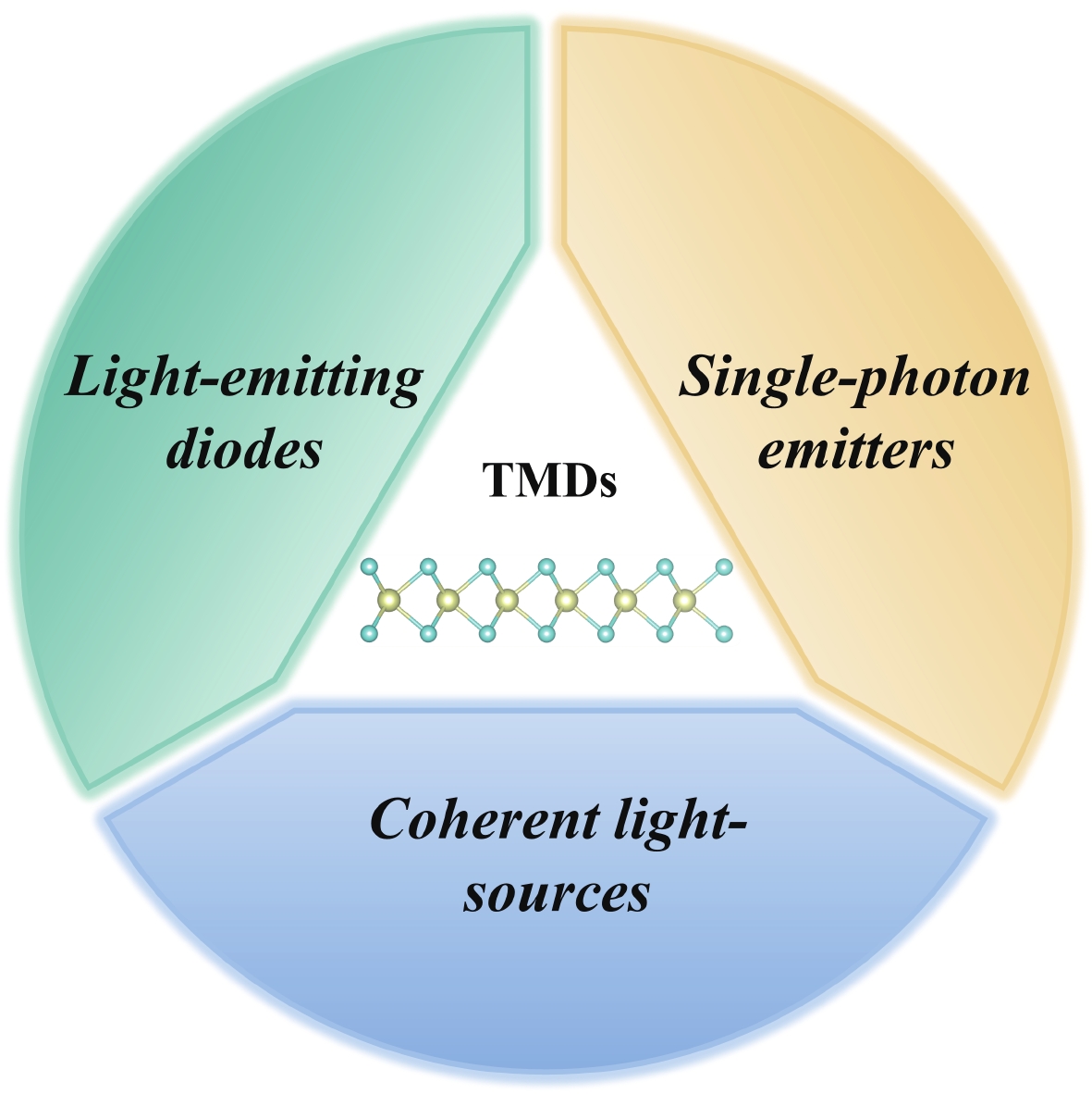
(Color online) Intriguing applications based on atomically thin MoSe2, including light-emitting diodes, single-photon emitters, and coherent light sources.
REVIEWS
Xinyu Zhang1, Xuewen Zhang1, Hanwei Hu1, Vanessa Li Zhang2, Weidong Xiao1, Guangchao Shi1, Jingyuan Qiao1, Nan Huang1, Ting Yu2, 3, and Jingzhi Shang1,
Corresponding author: Ting Yu, yu.ting@whu.edu.cn; Jingzhi Shang, iamjzshang@nwpu.edu.cn
Abstract: Atomically thin MoSe2 layers, as a core member of the transition metal dichalcogenides (TMDs) family, benefit from their appealing properties, including tunable band gaps, high exciton binding energies, and giant oscillator strengths, thus providing an intriguing platform for optoelectronic applications of light-emitting diodes (LEDs), field-effect transistors (FETs), single-photon emitters (SPEs), and coherent light sources (CLSs). Moreover, these MoSe2 layers can realize strong excitonic emission in the near-infrared wavelengths, which can be combined with the silicon-based integration technologies and further encourage the development of the new generation technologies of on-chip optical interconnection, quantum computing, and quantum information processing. Herein, we overview the state-of-the-art applications of light-emitting devices based on two-dimensional MoSe2 layers. Firstly, we introduce recent developments in excitonic emission features from atomically thin MoSe2 and their dependences on typical physical fields. Next, we focus on the exciton-polaritons and plasmon-exciton polaritons in MoSe2 coupled to the diverse forms of optical microcavities. Then, we highlight the promising applications of LEDs, SPEs, and CLSs based on MoSe2 and their heterostructures. Finally, we summarize the challenges and opportunities for high-quality emission of MoSe2 and high-performance light-emitting devices.
Key words: MoSe2, light−matter interaction, exciton, polariton, light-emitting device
| [1] |
Manzeli S, Ovchinnikov D, Pasquier D, et al. 2D transition metal dichalcogenides. Nat Rev Mater, 2017, 2(8), 17033 doi: 10.1038/natrevmats.2017.33
|
| [2] |
Wu X, Chen X Y, Yang R X, et al. Recent advances on tuning the interlayer coupling and properties in van der waals heterostructures. Small, 2022, 18(15), 2105877 doi: 10.1002/smll.202105877
|
| [3] |
Ou H, Matsuoka H, Tempia J, et al. Spatial control of dynamic p-i-n junctions in transition metal dichalcogenide light-emitting devices. ACS Nano, 2021, 15(8), 12911 doi: 10.1021/acsnano.1c01242
|
| [4] |
Chamlagain B, Li Q, Ghimire N J, et al. Mobility improvement and temperature dependence in MoSe2 field-effect transistors on parylene-C substrate. ACS Nano, 2014, 8(5), 5079 doi: 10.1021/nn501150r
|
| [5] |
Du W, Yu P, Zhu J T, et al. An ultrathin MoSe2 photodetector with near-perfect absorption. Nanotechnology, 2020, 31(22), 225201 doi: 10.1088/1361-6528/ab746f
|
| [6] |
Wen W, Wu L S, Yu T. Excitonic lasers in atomically thin 2D semiconductors. ACS Mater Lett, 2020, 2(10), 1328 doi: 10.1021/acsmaterialslett.0c00277
|
| [7] |
Fang H H, Han B, Robert C, et al. Control of the exciton radiative lifetime in van der waals heterostructures. Phys Rev Lett, 2019, 123(6), 067401 doi: 10.1103/PhysRevLett.123.067401
|
| [8] |
Zhang L, Wu F C, Hou S C, et al. Van der waals heterostructure polaritons with moiré-induced nonlinearity. Nature, 2021, 591(7848), 61 doi: 10.1038/s41586-021-03228-5
|
| [9] |
Jia S A, Jin Z H, Zhang J, et al. Lateral monolayer MoSe2-WSe2 p-n heterojunctions with giant built-in potentials. Small, 2020, 16(34), 2002263 doi: 10.1002/smll.202002263
|
| [10] |
Sun J W, Hu H T, Pan D, et al. Selectively depopulating valley-polarized excitons in monolayer MoS2 by local chirality in single plasmonic nanocavity. Nano Lett, 2020, 20(7), 4953 doi: 10.1021/acs.nanolett.0c01019
|
| [11] |
Henck H, Mauro D, Domaretskiy D, et al. Light sources with bias tunable spectrum based on van der waals interface transistors. Nat Commun, 2022, 13(1), 3917 doi: 10.1038/s41467-022-31605-9
|
| [12] |
Chen Y Y, Liu Z Y, Li J Z, et al. Robust interlayer coupling in two-dimensional perovskite/monolayer transition metal dichalcogenide heterostructures. ACS Nano, 2020, 14(8), 10258 doi: 10.1021/acsnano.0c03624
|
| [13] |
Chen Y Y, Liu Z Y, Li J Z, et al. Manipulation of valley pseudospin by selective spin injection in chiral two-dimensional perovskite/monolayer transition metal dichalcogenide heterostructures. ACS Nano, 2020, 14(11), 15154 doi: 10.1021/acsnano.0c05343
|
| [14] |
Yao W D, Yang D, Chen Y Y, et al. Layer-number engineered momentum-indirect interlayer excitons with large spectral tunability. Nano Lett, 2022, 22(17), 7230 doi: 10.1021/acs.nanolett.2c02742
|
| [15] |
Horng J, Stroucken T, Zhang L, et al. Observation of interlayer excitons in MoSe2 single crystals. Phys Rev B, 2018, 97(24), 241404 doi: 10.1103/PhysRevB.97.241404
|
| [16] |
Joe A Y, Jauregui L A, Pistunova K, et al. Electrically controlled emission from singlet and triplet exciton species in atomically thin light-emitting diodes. Phys Rev B, 2021, 103(16), L161411 doi: 10.1103/PhysRevB.103.L161411
|
| [17] |
Huang C M, Wu S F, Sanchez A M, et al. Lateral heterojunctions within monolayer MoSe2-WSe2 semiconductors. Nat Mater, 2014, 13(12), 1096 doi: 10.1038/nmat4064
|
| [18] |
Rivera P, Schaibley J R, Jones A M, et al. Observation of long-lived interlayer excitons in monolayer MoSe2-WSe2 heterostructures. Nat Commun, 2015, 6(1), 6242 doi: 10.1038/ncomms7242
|
| [19] |
Jin Y, Keum D H, An S J, et al. A van der waals homojunction: Ideal p-n diode behavior in MoSe2. Adv Mater, 2015, 27(37), 5534 doi: 10.1002/adma.201502278
|
| [20] |
Yu L, Deng M D, Zhang J L, et al. Site-controlled quantum emitters in monolayer MoSe2. Nano Lett, 2021, 21(6), 2376 doi: 10.1021/acs.nanolett.0c04282
|
| [21] |
Branny A, Wang G, Kumar S, et al. Discrete quantum dot like emitters in monolayer MoSe2: Spatial mapping, magneto-optics, and charge tuning. Appl Phys Lett, 2016, 108(14), 142101 doi: 10.1063/1.4945268
|
| [22] |
Paik E Y, Zhang L, Burg G W, et al. Interlayer exciton laser of extended spatial coherence in atomically thin heterostructures. Nature, 2019, 576(7785), 80 doi: 10.1038/s41586-019-1779-x
|
| [23] |
Anton-Solanas C, Waldherr M, Klaas M, et al. Bosonic condensation of exciton-polaritons in an atomically thin crystal. Nat Mater, 2021, 20(9), 1233 doi: 10.1038/s41563-021-01000-8
|
| [24] |
Li C Y, Wang Q F, Diao H, et al. Enhanced photoluminescence of monolayer MoSe2 in a double resonant plasmonic nanocavity with fano resonance and mode matching. Laser Photonics Rev, 2022, 16(2), 2100199 doi: 10.1002/lpor.202100199
|
| [25] |
Péchou R, Jia S A, Rigor J, et al. Plasmonic-induced luminescence of MoSe2 monolayers in a scanning tunneling microscope. ACS Photonics, 2020, 7(11), 3061 doi: 10.1021/acsphotonics.0c01101
|
| [26] |
Zhang Y X, Chen W, Fu T, et al. Simultaneous surface-enhanced resonant raman and fluorescence spectroscopy of monolayer MoSe2: Determination of ultrafast decay rates in nanometer dimension. Nano Lett, 2019, 19(9), 6284 doi: 10.1021/acs.nanolett.9b02425
|
| [27] |
Dufferwiel S, Schwarz S, Withers F, et al. Exciton-polaritons in van der waals heterostructures embedded in tunable microcavities. Nat Commun, 2015, 6(1), 8579 doi: 10.1038/ncomms9579
|
| [28] |
Kumar P, Lynch J, Song B K, et al. light−matter coupling in large-area van der waals superlattices. Nat Nanotechnol, 2022, 17(2), 182 doi: 10.1038/s41565-021-01023-x
|
| [29] |
Paik E Y, Zhang L, Hou S C, et al. High quality factor microcavity for van der waals semiconductor polaritons using a transferrable mirror. Adv Opt Mater, 2023, 11(1), 2201440 doi: 10.1002/adom.202201440
|
| [30] |
Park S, Kim D, Seo M K. Plasmonic photonic crystal mirror for long-lived interlayer exciton generation. ACS Photonics, 2021, 8(12), 3619 doi: 10.1021/acsphotonics.1c01243
|
| [31] |
Tanoh A O A, Alexander-Webber J, Fan Y, et al. Giant photoluminescence enhancement in MoSe2 monolayers treated with oleic acid ligands. Nanoscale Adv, 2021, 3(14), 4216 doi: 10.1039/D0NA01014F
|
| [32] |
Han H V, Lu A Y, Lu L S, et al. Photoluminescence enhancement and structure repairing of monolayer MoSe2 by hydrohalic acid treatment. ACS Nano, 2016, 10(1), 1454 doi: 10.1021/acsnano.5b06960
|
| [33] |
Lundt N, Maryński A, Cherotchenko E, et al. Monolayered MoSe2: A candidate for room temperature polaritonics. 2D Mater, 2017, 4(1), 015006 doi: 10.1088/2053-1583/4/1/015006
|
| [34] |
Gillard D J, Genco A, Ahn S, et al. Strong exciton-photon coupling in large area MoSe2 and WSe2 heterostructures fabricated from two-dimensional materials grown by chemical vapor deposition. 2D Mater, 2021, 8(1), 011002 doi: 10.1088/2053-1583/abc5a1
|
| [35] |
Wurdack M, Lundt N, Klaas M, et al. Observation of hybrid Tamm-plasmon exciton-polaritons with GaAs quantum wells and a MoSe2 monolayer. Nat Commun, 2017, 8(1), 259 doi: 10.1038/s41467-017-00155-w
|
| [36] |
Waldherr M, Lundt N, Klaas M, et al. Observation of bosonic condensation in a hybrid monolayer MoSe2-GaAs microcavity. Nat Commun, 2018, 9(1), 3286 doi: 10.1038/s41467-018-05532-7
|
| [37] |
Zhang Y, Chang T R, Zhou B, et al. Direct observation of the transition from indirect to direct bandgap in atomically thin epitaxial MoSe2. Nat Nanotechnol, 2014, 9(2), 111 doi: 10.1038/nnano.2013.277
|
| [38] |
Tongay S, Zhou J, Ataca C, et al. Thermally driven crossover from indirect toward direct bandgap in 2D semiconductors: MoSe2 versus MoS2. Nano Lett, 2012, 12(11), 5576 doi: 10.1021/nl302584w
|
| [39] |
Shi Y F, Hua C X, Li B, et al. Highly ordered mesoporous crystalline MoSe2 material with efficient visible-light-driven photocatalytic activity and enhanced lithium storage performance. Adv Funct Mater, 2013, 23(14), 1832 doi: 10.1002/adfm.201202144
|
| [40] |
Schneider C, Glazov M M, Korn T, et al. Two-dimensional semiconductors in the regime of strong light−matter coupling. Nat Commun, 2018, 9(1), 2695 doi: 10.1038/s41467-018-04866-6
|
| [41] |
Ye Z L, Cao T, O'Brien K, et al. Probing excitonic dark states in single-layer tungsten disulphide. Nature, 2014, 513(7517), 214 doi: 10.1038/nature13734
|
| [42] |
Echeverry J P, Urbaszek B, Amand T, et al. Splitting between bright and dark excitons in transition metal dichalcogenide monolayers. Phys Rev B, 2016, 93(12), 121107 doi: 10.1103/PhysRevB.93.121107
|
| [43] |
Hao K, Specht J F, Nagler P, et al. Neutral and charged inter-valley biexcitons in monolayer MoSe2. Nat Commun, 2017, 8(1), 15552 doi: 10.1038/ncomms15552
|
| [44] |
Mak K F, He K L, Lee C G, et al. Tightly bound trions in monolayer MoS2. Nat Mater, 2013, 12(3), 207 doi: 10.1038/nmat3505
|
| [45] |
Rivera P, Yu H Y, Seyler K L, et al. Interlayer valley excitons in heterobilayers of transition metal dichalcogenides. Nat Nanotechnol, 2018, 13(11), 1004 doi: 10.1038/s41565-018-0193-0
|
| [46] |
Datta B, Khatoniar M, Deshmukh P, et al. Highly nonlinear dipolar exciton-polaritons in bilayer MoS2. Nat Commun, 2022, 13(1), 6341 doi: 10.1038/s41467-022-33940-3
|
| [47] |
Pei J J, Yang J, Wang X B, et al. Excited state biexcitons in atomically thin MoSe2. ACS Nano, 2017, 11(7), 7468 doi: 10.1021/acsnano.7b03909
|
| [48] |
Godde T, Schmidt D, Schmutzler J, et al. Exciton and trion dynamics in atomically thin MoSe2 and WSe2: Effect of localization. Phys Rev B, 2016, 94(16), 165301 doi: 10.1103/PhysRevB.94.165301
|
| [49] |
Wang J A, Huang J H, Li Y H, et al. Radiative and non-radiative exciton recombination processes in a chemical vapor deposition-grown MoSe2 film. J Phys Chem C, 2022, 126(36), 15319 doi: 10.1021/acs.jpcc.2c04550
|
| [50] |
Yu Y F, Yu Y L, Xu C, et al. Engineering substrate interactions for high luminescence efficiency of transition-metal dichalcogenide monolayers. Adv Funct Mater, 2016, 26(26), 4733 doi: 10.1002/adfm.201600418
|
| [51] |
Wierzbowski J, Klein J, Sigger F, et al. Direct exciton emission from atomically thin transition metal dichalcogenide heterostructures near the lifetime limit. Sci Rep, 2017, 7(1), 12383 doi: 10.1038/s41598-017-09739-4
|
| [52] |
Grzeszczyk M, Molas M R, Nogajewski K, et al. The effect of metallic substrates on the optical properties of monolayer MoSe2. Sci Rep, 2020, 10(1), 4981 doi: 10.1038/s41598-020-61673-0
|
| [53] |
Ciarrocchi A, Unuchek D, Avsar A, et al. Polarization switching and electrical control of interlayer excitons in two-dimensional van der waals heterostructures. Nat Photonics, 2019, 13(2), 131 doi: 10.1038/s41566-018-0325-y
|
| [54] |
Hagel J, Brem S, Malic E. Electrical tuning of moiré excitons in MoSe2 bilayers. 2D Mater, 2023, 10(1), 014013 doi: 10.1088/2053-1583/aca916
|
| [55] |
Lu Z G, Rhodes D, Li Z P, et al. Magnetic field mixing and splitting of bright and dark excitons in monolayer MoSe2. 2D Mater, 2020, 7(1), 015017 doi: 10.1088/2053-1583/ab5614
|
| [56] |
Robert C, Han B, Kapuscinski P, et al. Measurement of the spin-forbidden dark excitons in MoS2 and MoSe2 monolayers. Nat Commun, 2020, 11(1), 4037 doi: 10.1038/s41467-020-17608-4
|
| [57] |
Ross J S, Wu S F, Yu H Y, et al. Electrical control of neutral and charged excitons in a monolayer semiconductor. Nat Commun, 2013, 4(1), 1474 doi: 10.1038/ncomms2498
|
| [58] |
Tang Y H, Gu J, Liu S, et al. Tuning layer-hybridized moiré excitons by the quantum-confined Stark effect. Nat Nanotechnol, 2021, 16(1), 52 doi: 10.1038/s41565-020-00783-2
|
| [59] |
Shim G W, Yoo K, Seo S B, et al. Large-area single-layer MoSe2 and its van der waals heterostructures. ACS Nano, 2014, 8(7), 6655 doi: 10.1021/nn405685j
|
| [60] |
Du W N, Zhang S A, Zhang Q, et al. Recent progress of strong exciton-photon coupling in lead halide perovskites. Adv Mater, 2019, 31(45), 1804894 doi: 10.1002/adma.201804894
|
| [61] |
Zhao L Y, Shang Q Y, Li M L, et al. Strong exciton-photon interaction and lasing of two-dimensional transition metal dichalcogenide semiconductors. Nano Res, 2021, 14(6), 1937 doi: 10.1007/s12274-020-3073-5
|
| [62] |
Purcell E M, Torrey H C, Pound R V. Resonance absorption by nuclear magnetic moments in a solid. Phys Rev, 1946, 69, 37 doi: 10.1103/PhysRev.69.37
|
| [63] |
Shang J Z, Cong C X, Wang Z L, et al. Room-temperature 2D semiconductor activated vertical-cavity surface-emitting lasers. Nat Commun, 2017, 8(1), 543 doi: 10.1038/s41467-017-00743-w
|
| [64] |
Lozano G, Rodriguez S R, Verschuuren M A, et al. Metallic nanostructures for efficient LED lighting. Light Sci Appl, 2016, 5(6), e16080 doi: 10.1038/lsa.2016.80
|
| [65] |
Schuler B, Cochrane K A, Kastl C, et al. Electrically driven photon emission from individual atomic defects in monolayer WS2. Sci Adv, 2020, 6(38), eabb5988 doi: 10.1126/sciadv.abb5988
|
| [66] |
Englund D, Fattal D, Waks E, et al. Controlling the spontaneous emission rate of single quantum dots in a two-dimensional photonic crystal. Phys Rev Lett, 2005, 95(1), 013904 doi: 10.1103/PhysRevLett.95.013904
|
| [67] |
Wang Z, Dong Z G, Gu Y H, et al. Giant photoluminescence enhancement in tungsten-diselenide-gold plasmonic hybrid structures. Nat Commun, 2016, 7(1), 11283 doi: 10.1038/ncomms11283
|
| [68] |
Pelton M. Modified spontaneous emission in nanophotonic structures. Nat Photonics, 2015, 9(7), 427 doi: 10.1038/nphoton.2015.103
|
| [69] |
Kim J H, Lee H S, An G H, et al. Dielectric nanowire hybrids for plasmon-enhanced light−matter interaction in 2D semiconductors. ACS Nano, 2020, 14(9), 11985 doi: 10.1021/acsnano.0c05158
|
| [70] |
Husko C, Kang J, Moille G, et al. Silicon-phosphorene nanocavity-enhanced optical emission at telecommunications wavelengths. Nano Lett, 2018, 18(10), 6515 doi: 10.1021/acs.nanolett.8b03037
|
| [71] |
Gerard J M, Gayral B. Strong Purcell effect for InAs quantum boxes in three-dimensional solid-state microcavities. J Light Technol, 1999, 17(11), 2089 doi: 10.1109/50.802999
|
| [72] |
Lepeshov S, Krasnok A, Alù A. Enhanced excitation and emission from 2D transition metal dichalcogenides with all-dielectric nanoantennas. Nanotechnology, 2019, 30(25), 254004 doi: 10.1088/1361-6528/ab0daf
|
| [73] |
Weisbuch C, Nishioka M, Ishikawa A, et al. Observation of the coupled exciton-photon mode splitting in a semiconductor quantum microcavity. Phys Rev Lett, 1992, 69(23), 3314 doi: 10.1103/PhysRevLett.69.3314
|
| [74] |
Deng H, Haug H, Yamamoto Y. Exciton-polariton bose-einstein condensation. Rev Mod Phys, 2010, 82(2), 1489 doi: 10.1103/RevModPhys.82.1489
|
| [75] |
Lackner L, Dusel M, Egorov O A, et al. Tunable exciton-polaritons emerging from WS2 monolayer excitons in a photonic lattice at room temperature. Nat Commun, 2021, 12(1), 4933 doi: 10.1038/s41467-021-24925-9
|
| [76] |
Wurdack M, Estrecho E, Todd S, et al. Motional narrowing, ballistic transport, and trapping of room-temperature exciton polaritons in an atomically-thin semiconductor. Nat Commun, 2021, 12(1), 5366 doi: 10.1038/s41467-021-25656-7
|
| [77] |
Jiang Z J, Ren A, Yan Y L, et al. Exciton-polaritons and their bose-einstein condensates in organic semiconductor microcavities. Adv Mater, 2022, 34(4), 2106095 doi: 10.1002/adma.202106095
|
| [78] |
Munkhbat B, Baranov D G, Stührenberg M, et al. Self-hybridized exciton-polaritons in multilayers of transition metal dichalcogenides for efficient light absorption. ACS Photonics, 2019, 6(1), 139 doi: 10.1021/acsphotonics.8b01194
|
| [79] |
Shang J Z, Zhang X Y, Zhang V L, et al. Exciton-photon interactions in two-dimensional semiconductor microcavities. ACS Photonics, 2023, 10, 7, 2064 doi: 10.1021/acsphotonics.2c01541
|
| [80] |
Liu X Z, Galfsky T, Sun Z, et al. Strong light−matter coupling in two-dimensional atomic crystals. Nat Photonics, 2015, 9(1), 30 doi: 10.1038/nphoton.2014.304
|
| [81] |
Li Q Y, Alfrey A, Hu J Q, et al. Macroscopic transition metal dichalcogenides monolayers with uniformly high optical quality. Nat Commun, 2023, 14(1), 1837 doi: 10.1038/s41467-023-37500-1
|
| [82] |
Dufferwiel S, Lyons T P, Solnyshkov D D, et al. Valley-addressable polaritons in atomically thin semiconductors. Nat Photonics, 2017, 11(8), 497 doi: 10.1038/nphoton.2017.125
|
| [83] |
Ajayi O A, Ardelean J V, Shepard G D, et al. Approaching the intrinsic photoluminescence linewidth in transition metal dichalcogenide monolayers. 2D Mater, 2017, 4(3), 031011 doi: 10.1088/2053-1583/aa6aa1
|
| [84] |
Del Pozo-Zamudio O, Genco A, Schwarz S, et al. Electrically pumped WSe2-based light-emitting van der Waals heterostructures embedded in monolithic dielectric microcavities. 2D Mater, 2020, 7(3), 031006 doi: 10.1088/2053-1583/ab8542
|
| [85] |
Slootsky M, Liu X Z, Menon V M, et al. Room temperature frenkel-wannier-mott hybridization of degenerate excitons in a strongly coupled microcavity. Phys Rev Lett, 2014, 112(7), 076401 doi: 10.1103/PhysRevLett.112.076401
|
| [86] |
Zheng D, Zhang S P, Deng Q, et al. Manipulating coherent plasmon-exciton interaction in a single silver nanorod on monolayer WSe2. Nano Lett, 2017, 17(6), 3809 doi: 10.1021/acs.nanolett.7b01176
|
| [87] |
Sun J W, Li Y, Hu H T, et al. Strong plasmon-exciton coupling in transition metal dichalcogenides and plasmonic nanostructures. Nanoscale, 2021, 13(8), 4408 doi: 10.1039/D0NR08592H
|
| [88] |
Wen J X, Wang H, Wang W L, et al. Room-temperature strong light−matter interaction with active control in single plasmonic nanorod coupled with two-dimensional atomic crystals. Nano Lett, 2017, 17(8), 4689 doi: 10.1021/acs.nanolett.7b01344
|
| [89] |
Liu W J, Lee B, Naylor C H, et al. Strong exciton-plasmon coupling in MoS2 coupled with plasmonic lattice. Nano Lett, 2016, 16(2), 1262 doi: 10.1021/acs.nanolett.5b04588
|
| [90] |
Petrić M M, Kremser M, Barbone M, et al. Tuning the optical properties of a MoSe2 monolayer using nanoscale plasmonic antennas. Nano Lett, 2022, 22(2), 561 doi: 10.1021/acs.nanolett.1c02676
|
| [91] |
Lundt N, Klembt S, Cherotchenko E, et al. Room-temperature tamm-plasmon exciton-polaritons with a WSe2 monolayer. Nat Commun, 2016, 7(1), 13328 doi: 10.1038/ncomms13328
|
| [92] |
Hu F R, Fei Z. Recent progress on exciton polaritons in layered transition-metal dichalcogenides. Adv Opt Mater, 2020, 8(5), 1901003 doi: 10.1002/adom.201901003
|
| [93] |
Kaliteevski M, Iorsh I, Brand S, et al. Tamm plasmon-polaritons: Possible electromagnetic states at the interface of a metal and a dielectric Bragg mirror. Phys Rev B, 2007, 76(16), 165415 doi: 10.1103/PhysRevB.76.165415
|
| [94] |
Lundt N, Nagler P, Nalitov A, et al. Valley polarized relaxation and upconversion luminescence from Tamm-plasmon trion-polaritons with a MoSe2 monolayer. 2D Mater, 2017, 4(2), 025096 doi: 10.1088/2053-1583/aa6ef2
|
| [95] |
Low T, Chaves A, Caldwell J D, et al. Polaritons in layered two-dimensional materials. Nat Mater, 2017, 16(2), 182 doi: 10.1038/nmat4792
|
| [96] |
Guo X D, Lyu W, Chen T H, et al. Polaritons in van der waals heterostructures. Adv Mater, 2023, 35, 2201856 doi: 10.1002/adma.202201856
|
| [97] |
Liu D S, Wu J A, Xu H X, et al. Emerging light-emitting materials for photonic integration. Adv Mater, 2021, 33(4), 2003733 doi: 10.1002/adma.202003733
|
| [98] |
Wu J H, Ma H, Yin P, et al. Two-dimensional materials for integrated photonics: Recent advances and future challenges. Small Sci, 2021, 1(4), 2000053 doi: 10.1002/smsc.202000053
|
| [99] |
Xiao D, Liu G B, Feng W X, et al. Coupled spin and valley physics in monolayers of MoS2 and other group-VI dichalcogenides. Phys Rev Lett, 2012, 108(19), 196802 doi: 10.1103/PhysRevLett.108.196802
|
| [100] |
Wang Q H, Kalantar-Zadeh K, Kis A, et al. Electronics and optoelectronics of two-dimensional transition metal dichalcogenides. Nat Nanotechnol, 2012, 7(11), 699 doi: 10.1038/nnano.2012.193
|
| [101] |
Gu J, Chakraborty B, Khatoniar M, et al. A room-temperature polariton light-emitting diode based on monolayer WS2. Nat Nanotechnol, 2019, 14(11), 1024 doi: 10.1038/s41565-019-0543-6
|
| [102] |
Ross J S, Klement P, Jones A M, et al. Electrically tunable excitonic light-emitting diodes based on monolayer WSe2 p-n junctions. Nat Nanotechnol, 2014, 9(4), 268 doi: 10.1038/nnano.2014.26
|
| [103] |
Aftab S, Hegazy H H, Iqbal M Z, et al. Recent advances in dynamic homojunction PIN diodes based on 2D materials. Adv Mater Interfaces, 2023, 10(6), 2201937 doi: 10.1002/admi.202201937
|
| [104] |
Huang J K, Pu J A, Hsu C L, et al. Large-area synthesis of highly crystalline WSe2 monolayers and device applications. ACS Nano, 2014, 8(1), 923 doi: 10.1021/nn405719x
|
| [105] |
Chang Y H, Zhang W J, Zhu Y H, et al. Monolayer MoSe2 grown by chemical vapor deposition for fast photodetection. ACS Nano, 2014, 8(8), 8582 doi: 10.1021/nn503287m
|
| [106] |
Iqbal M W, Iqbal M Z, Khan M F, et al. High-mobility and air-stable single-layer WS2 field-effect transistors sandwiched between chemical vapor deposition-grown hexagonal BN films. Sci Rep, 2015, 5(1), 10699 doi: 10.1038/srep10699
|
| [107] |
Sajid A, Ford M J, Reimers J R. Single-photon emitters in hexagonal boron nitride: A review of progress. Rep Prog Phys, 2020, 83(4), 044501 doi: 10.1088/1361-6633/ab6310
|
| [108] |
Cai J M, Retzker A, Jelezko F, et al. A large-scale quantum simulator on a diamond surface at room temperature. Nat Phys, 2013, 9(3), 168 doi: 10.1038/nphys2519
|
| [109] |
Lee J Y, Leong V, Kalashnikov D, et al. Integrated single photon emitters. AVS Quantum Sci, 2020, 2(3), 031701 doi: 10.1116/5.0011316
|
| [110] |
Arakawa Y, Holmes M J. Progress in quantum-dot single photon sources for quantum information technologies: A broad spectrum overview. Appl Phys Rev, 2020, 7(2), 021309 doi: 10.1063/5.0010193
|
| [111] |
Atatüre M, Englund D, Vamivakas N, et al. Material platforms for spin-based photonic quantum technologies. Nat Rev Mater, 2018, 3(5), 38 doi: 10.1038/s41578-018-0008-9
|
| [112] |
Chakraborty C, Kinnischtzke L, Goodfellow K M, et al. Voltage-controlled quantum light from an atomically thin semiconductor. Nat Nanotechnol, 2015, 10(6), 507 doi: 10.1038/nnano.2015.79
|
| [113] |
Peng L T, Chan H, Choo P, et al. Creation of single-photon emitters in WSe2 monolayers using nanometer-sized gold tips. Nano Lett, 2020, 20(8), 5866 doi: 10.1021/acs.nanolett.0c01789
|
| [114] |
Parto K, Azzam S I, Banerjee K, et al. Defect and strain engineering of monolayer WSe2 enables site-controlled single-photon emission up to 150 K. Nat Commun, 2021, 12(1), 3585 doi: 10.1038/s41467-021-23709-5
|
| [115] |
Dass C K, Khan M A, Clark G, et al. Ultra-long lifetimes of single quantum emitters in monolayer WSe2/hBN heterostructures. Adv Quantum Technol, 2019, 2(5-6), 1900022 doi: 10.1002/qute.201900022
|
| [116] |
Michaelis de Vasconcellos S, Wigger D, Wurstbauer U, et al. Single-photon emitters in layered van der waals materials. Phys Status Solidi B, 2022, 259(4), 2100566 doi: 10.1002/pssb.202100566
|
| [117] |
Koperski M, Nogajewski K, Arora A, et al. Single photon emitters in exfoliated WSe2 structures. Nat Nanotechnol, 2015, 10(6), 503 doi: 10.1038/nnano.2015.67
|
| [118] |
Srivastava A, Sidler M, Allain A V, et al. Optically active quantum dots in monolayer WSe2. Nat Nanotechnol, 2015, 10(6), 491 doi: 10.1038/nnano.2015.60
|
| [119] |
Schwarz S, Kozikov A, Withers F, et al. Electrically pumped single-defect light emitters in WSe2. 2D Mater, 2016, 3(2), 025038 doi: 10.1088/2053-1583/3/2/025038
|
| [120] |
Chakraborty C, Goodfellow K M, Nick Vamivakas A. Localized emission from defects in MoSe2 layers. Opt Mater Express, 2016, 6(6), 2081 doi: 10.1364/OME.6.002081
|
| [121] |
Baek H, Brotons-Gisbert M, Koong Z X, et al. Highly energy-tunable quantum light from moiré-trapped excitons. Sci Adv, 2020, 6(37), eaba8526 doi: 10.1126/sciadv.aba8526
|
| [122] |
Kim S, Zhang B, Wang Z R, et al. Coherent polariton laser. Phys Rev X, 2016, 6(1), 011026 doi: 10.1103/PhysRevX.6.011026
|
| [123] |
Deng H, Weihs G, Snoke D, et al. Polariton lasing vs. photon lasing in a semiconductor microcavity. Proc Natl Acad Sci, 2003, 100(26), 15318 doi: 10.1073/pnas.2634328100
|
| [124] |
Wang C Y, Kang Z, Zheng Z, et al. Monolayer MoSe2/NiO van der Waals heterostructures for infrared light-emitting diodes. J Mater Chem C, 2019, 7(43), 13613 doi: 10.1039/C9TC04481G
|
| [125] |
Chen Z X, Liu H Q, Chen X C, et al. Wafer-size and single-crystal MoSe2 atomically thin films grown on GaN substrate for light emission and harvesting. ACS Appl Mater Interfaces, 2016, 8(31), 20267 doi: 10.1021/acsami.6b04768
|

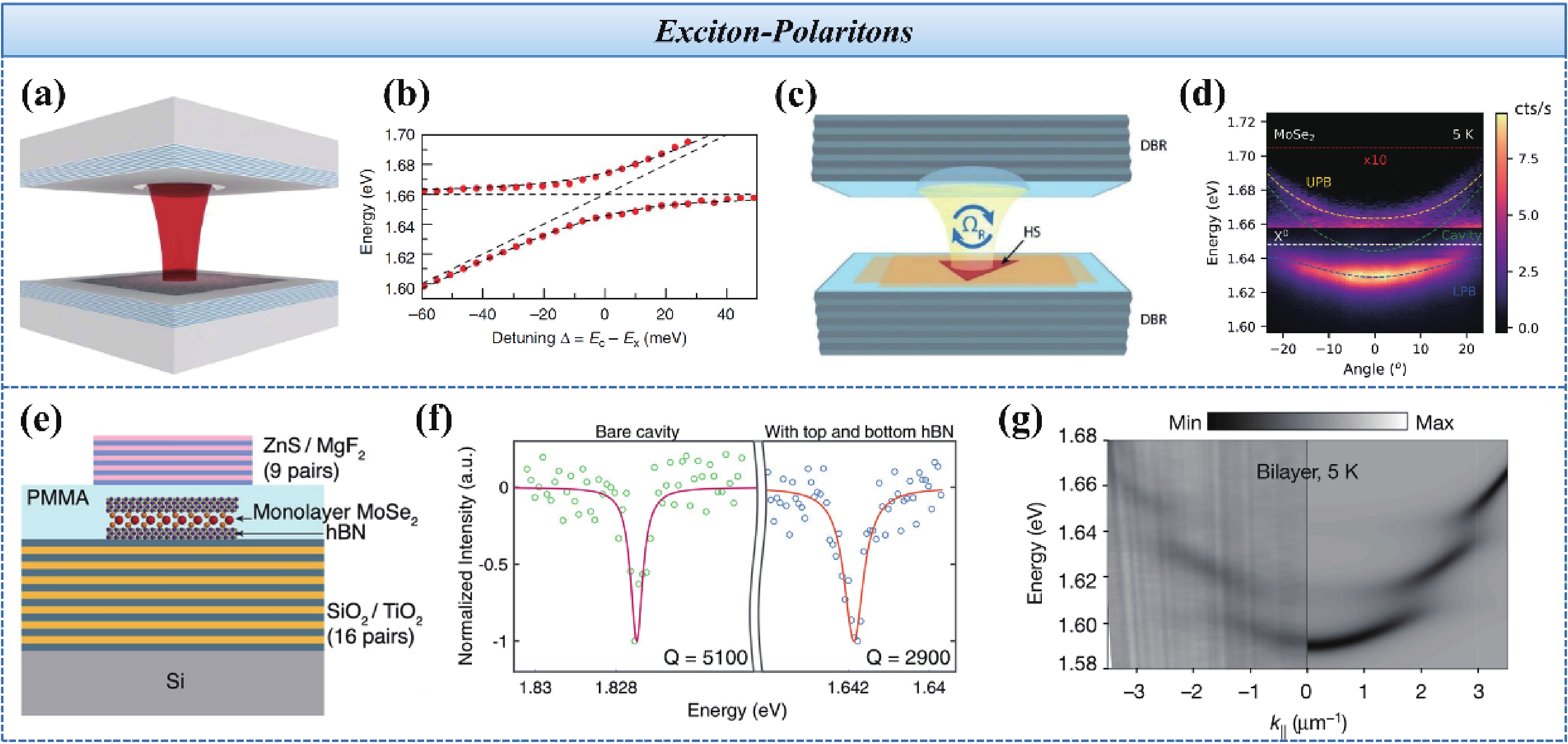

Table 1. Strong coupling regime in atomically thin MoSe2.
| Materials | Preparation technique of MoSe2 | Microcavity type | T (K) | Rabi splitting (2hΩ)/ coupling strength (g) | Ref. |
| 1L MoSe2 | Mechanical exfoliation | Open cavity | 4 | 17.5 meV | [33] |
| F−P cavity | 4 | 29.3 meV | |||
| 1-dodecanol/1L MoSe2/1-dodecanol | Mechanical exfoliation | Photonic crystal cavity | 5 | 43 ± 3 meV | [81] |
| 1L MoSe2/h-BN | Mechanical exfoliation | F−P cavity | 4.2 | 20 meV | [27] |
| MoSe2/h-BN/MoSe2/h-BN | 29 meV | ||||
| 1L MoSe2/h-BN | CVD growth | Open cavity | 4 | 17 meV | [34] |
| F−P cavity | 5 | 34 ± 4 meV | |||
| F−P cavity | 150 | 31 ± 4 meV | |||
| MoSe2/WS2 | Mechanical exfoliation | F−P cavity | 4 | g is 17.1 ± 0.1 | [8] |
| h-BN/1L MoSe2/h-BN | Mechanical exfoliation | F−P cavity | 4.2 | 15.2 ± 0.1 meV | [82] |
| h-BN/1L MoSe2/h-BN | Mechanical exfoliation | F−P cavity | 5 | 28 meV | [29] |
| 1L MoSe2-GaAs quantum wells | Mechanical exfoliation | Tamm cavity | 4 | g is 20 | [35] |
| 1L MoSe2-GaAs quantum wells | Mechanical exfoliation | Tamm cavity | 4.2 | g is 20 | [36] |
| h-BN/1L MoSe2-GaAs quantum well | CVD growth | F−P cavity | 4 | 25 ± 2 meV | [23] |
| 1L MoSe2 | Mechanical exfoliation | Tamm cavity | 4 | 33.5 meV | [33] |
 DownLoad: CSV
| [1] |
Manzeli S, Ovchinnikov D, Pasquier D, et al. 2D transition metal dichalcogenides. Nat Rev Mater, 2017, 2(8), 17033 doi: 10.1038/natrevmats.2017.33
|
| [2] |
Wu X, Chen X Y, Yang R X, et al. Recent advances on tuning the interlayer coupling and properties in van der waals heterostructures. Small, 2022, 18(15), 2105877 doi: 10.1002/smll.202105877
|
| [3] |
Ou H, Matsuoka H, Tempia J, et al. Spatial control of dynamic p-i-n junctions in transition metal dichalcogenide light-emitting devices. ACS Nano, 2021, 15(8), 12911 doi: 10.1021/acsnano.1c01242
|
| [4] |
Chamlagain B, Li Q, Ghimire N J, et al. Mobility improvement and temperature dependence in MoSe2 field-effect transistors on parylene-C substrate. ACS Nano, 2014, 8(5), 5079 doi: 10.1021/nn501150r
|
| [5] |
Du W, Yu P, Zhu J T, et al. An ultrathin MoSe2 photodetector with near-perfect absorption. Nanotechnology, 2020, 31(22), 225201 doi: 10.1088/1361-6528/ab746f
|
| [6] |
Wen W, Wu L S, Yu T. Excitonic lasers in atomically thin 2D semiconductors. ACS Mater Lett, 2020, 2(10), 1328 doi: 10.1021/acsmaterialslett.0c00277
|
| [7] |
Fang H H, Han B, Robert C, et al. Control of the exciton radiative lifetime in van der waals heterostructures. Phys Rev Lett, 2019, 123(6), 067401 doi: 10.1103/PhysRevLett.123.067401
|
| [8] |
Zhang L, Wu F C, Hou S C, et al. Van der waals heterostructure polaritons with moiré-induced nonlinearity. Nature, 2021, 591(7848), 61 doi: 10.1038/s41586-021-03228-5
|
| [9] |
Jia S A, Jin Z H, Zhang J, et al. Lateral monolayer MoSe2-WSe2 p-n heterojunctions with giant built-in potentials. Small, 2020, 16(34), 2002263 doi: 10.1002/smll.202002263
|
| [10] |
Sun J W, Hu H T, Pan D, et al. Selectively depopulating valley-polarized excitons in monolayer MoS2 by local chirality in single plasmonic nanocavity. Nano Lett, 2020, 20(7), 4953 doi: 10.1021/acs.nanolett.0c01019
|
| [11] |
Henck H, Mauro D, Domaretskiy D, et al. Light sources with bias tunable spectrum based on van der waals interface transistors. Nat Commun, 2022, 13(1), 3917 doi: 10.1038/s41467-022-31605-9
|
| [12] |
Chen Y Y, Liu Z Y, Li J Z, et al. Robust interlayer coupling in two-dimensional perovskite/monolayer transition metal dichalcogenide heterostructures. ACS Nano, 2020, 14(8), 10258 doi: 10.1021/acsnano.0c03624
|
| [13] |
Chen Y Y, Liu Z Y, Li J Z, et al. Manipulation of valley pseudospin by selective spin injection in chiral two-dimensional perovskite/monolayer transition metal dichalcogenide heterostructures. ACS Nano, 2020, 14(11), 15154 doi: 10.1021/acsnano.0c05343
|
| [14] |
Yao W D, Yang D, Chen Y Y, et al. Layer-number engineered momentum-indirect interlayer excitons with large spectral tunability. Nano Lett, 2022, 22(17), 7230 doi: 10.1021/acs.nanolett.2c02742
|
| [15] |
Horng J, Stroucken T, Zhang L, et al. Observation of interlayer excitons in MoSe2 single crystals. Phys Rev B, 2018, 97(24), 241404 doi: 10.1103/PhysRevB.97.241404
|
| [16] |
Joe A Y, Jauregui L A, Pistunova K, et al. Electrically controlled emission from singlet and triplet exciton species in atomically thin light-emitting diodes. Phys Rev B, 2021, 103(16), L161411 doi: 10.1103/PhysRevB.103.L161411
|
| [17] |
Huang C M, Wu S F, Sanchez A M, et al. Lateral heterojunctions within monolayer MoSe2-WSe2 semiconductors. Nat Mater, 2014, 13(12), 1096 doi: 10.1038/nmat4064
|
| [18] |
Rivera P, Schaibley J R, Jones A M, et al. Observation of long-lived interlayer excitons in monolayer MoSe2-WSe2 heterostructures. Nat Commun, 2015, 6(1), 6242 doi: 10.1038/ncomms7242
|
| [19] |
Jin Y, Keum D H, An S J, et al. A van der waals homojunction: Ideal p-n diode behavior in MoSe2. Adv Mater, 2015, 27(37), 5534 doi: 10.1002/adma.201502278
|
| [20] |
Yu L, Deng M D, Zhang J L, et al. Site-controlled quantum emitters in monolayer MoSe2. Nano Lett, 2021, 21(6), 2376 doi: 10.1021/acs.nanolett.0c04282
|
| [21] |
Branny A, Wang G, Kumar S, et al. Discrete quantum dot like emitters in monolayer MoSe2: Spatial mapping, magneto-optics, and charge tuning. Appl Phys Lett, 2016, 108(14), 142101 doi: 10.1063/1.4945268
|
| [22] |
Paik E Y, Zhang L, Burg G W, et al. Interlayer exciton laser of extended spatial coherence in atomically thin heterostructures. Nature, 2019, 576(7785), 80 doi: 10.1038/s41586-019-1779-x
|
| [23] |
Anton-Solanas C, Waldherr M, Klaas M, et al. Bosonic condensation of exciton-polaritons in an atomically thin crystal. Nat Mater, 2021, 20(9), 1233 doi: 10.1038/s41563-021-01000-8
|
| [24] |
Li C Y, Wang Q F, Diao H, et al. Enhanced photoluminescence of monolayer MoSe2 in a double resonant plasmonic nanocavity with fano resonance and mode matching. Laser Photonics Rev, 2022, 16(2), 2100199 doi: 10.1002/lpor.202100199
|
| [25] |
Péchou R, Jia S A, Rigor J, et al. Plasmonic-induced luminescence of MoSe2 monolayers in a scanning tunneling microscope. ACS Photonics, 2020, 7(11), 3061 doi: 10.1021/acsphotonics.0c01101
|
| [26] |
Zhang Y X, Chen W, Fu T, et al. Simultaneous surface-enhanced resonant raman and fluorescence spectroscopy of monolayer MoSe2: Determination of ultrafast decay rates in nanometer dimension. Nano Lett, 2019, 19(9), 6284 doi: 10.1021/acs.nanolett.9b02425
|
| [27] |
Dufferwiel S, Schwarz S, Withers F, et al. Exciton-polaritons in van der waals heterostructures embedded in tunable microcavities. Nat Commun, 2015, 6(1), 8579 doi: 10.1038/ncomms9579
|
| [28] |
Kumar P, Lynch J, Song B K, et al. light−matter coupling in large-area van der waals superlattices. Nat Nanotechnol, 2022, 17(2), 182 doi: 10.1038/s41565-021-01023-x
|
| [29] |
Paik E Y, Zhang L, Hou S C, et al. High quality factor microcavity for van der waals semiconductor polaritons using a transferrable mirror. Adv Opt Mater, 2023, 11(1), 2201440 doi: 10.1002/adom.202201440
|
| [30] |
Park S, Kim D, Seo M K. Plasmonic photonic crystal mirror for long-lived interlayer exciton generation. ACS Photonics, 2021, 8(12), 3619 doi: 10.1021/acsphotonics.1c01243
|
| [31] |
Tanoh A O A, Alexander-Webber J, Fan Y, et al. Giant photoluminescence enhancement in MoSe2 monolayers treated with oleic acid ligands. Nanoscale Adv, 2021, 3(14), 4216 doi: 10.1039/D0NA01014F
|
| [32] |
Han H V, Lu A Y, Lu L S, et al. Photoluminescence enhancement and structure repairing of monolayer MoSe2 by hydrohalic acid treatment. ACS Nano, 2016, 10(1), 1454 doi: 10.1021/acsnano.5b06960
|
| [33] |
Lundt N, Maryński A, Cherotchenko E, et al. Monolayered MoSe2: A candidate for room temperature polaritonics. 2D Mater, 2017, 4(1), 015006 doi: 10.1088/2053-1583/4/1/015006
|
| [34] |
Gillard D J, Genco A, Ahn S, et al. Strong exciton-photon coupling in large area MoSe2 and WSe2 heterostructures fabricated from two-dimensional materials grown by chemical vapor deposition. 2D Mater, 2021, 8(1), 011002 doi: 10.1088/2053-1583/abc5a1
|
| [35] |
Wurdack M, Lundt N, Klaas M, et al. Observation of hybrid Tamm-plasmon exciton-polaritons with GaAs quantum wells and a MoSe2 monolayer. Nat Commun, 2017, 8(1), 259 doi: 10.1038/s41467-017-00155-w
|
| [36] |
Waldherr M, Lundt N, Klaas M, et al. Observation of bosonic condensation in a hybrid monolayer MoSe2-GaAs microcavity. Nat Commun, 2018, 9(1), 3286 doi: 10.1038/s41467-018-05532-7
|
| [37] |
Zhang Y, Chang T R, Zhou B, et al. Direct observation of the transition from indirect to direct bandgap in atomically thin epitaxial MoSe2. Nat Nanotechnol, 2014, 9(2), 111 doi: 10.1038/nnano.2013.277
|
| [38] |
Tongay S, Zhou J, Ataca C, et al. Thermally driven crossover from indirect toward direct bandgap in 2D semiconductors: MoSe2 versus MoS2. Nano Lett, 2012, 12(11), 5576 doi: 10.1021/nl302584w
|
| [39] |
Shi Y F, Hua C X, Li B, et al. Highly ordered mesoporous crystalline MoSe2 material with efficient visible-light-driven photocatalytic activity and enhanced lithium storage performance. Adv Funct Mater, 2013, 23(14), 1832 doi: 10.1002/adfm.201202144
|
| [40] |
Schneider C, Glazov M M, Korn T, et al. Two-dimensional semiconductors in the regime of strong light−matter coupling. Nat Commun, 2018, 9(1), 2695 doi: 10.1038/s41467-018-04866-6
|
| [41] |
Ye Z L, Cao T, O'Brien K, et al. Probing excitonic dark states in single-layer tungsten disulphide. Nature, 2014, 513(7517), 214 doi: 10.1038/nature13734
|
| [42] |
Echeverry J P, Urbaszek B, Amand T, et al. Splitting between bright and dark excitons in transition metal dichalcogenide monolayers. Phys Rev B, 2016, 93(12), 121107 doi: 10.1103/PhysRevB.93.121107
|
| [43] |
Hao K, Specht J F, Nagler P, et al. Neutral and charged inter-valley biexcitons in monolayer MoSe2. Nat Commun, 2017, 8(1), 15552 doi: 10.1038/ncomms15552
|
| [44] |
Mak K F, He K L, Lee C G, et al. Tightly bound trions in monolayer MoS2. Nat Mater, 2013, 12(3), 207 doi: 10.1038/nmat3505
|
| [45] |
Rivera P, Yu H Y, Seyler K L, et al. Interlayer valley excitons in heterobilayers of transition metal dichalcogenides. Nat Nanotechnol, 2018, 13(11), 1004 doi: 10.1038/s41565-018-0193-0
|
| [46] |
Datta B, Khatoniar M, Deshmukh P, et al. Highly nonlinear dipolar exciton-polaritons in bilayer MoS2. Nat Commun, 2022, 13(1), 6341 doi: 10.1038/s41467-022-33940-3
|
| [47] |
Pei J J, Yang J, Wang X B, et al. Excited state biexcitons in atomically thin MoSe2. ACS Nano, 2017, 11(7), 7468 doi: 10.1021/acsnano.7b03909
|
| [48] |
Godde T, Schmidt D, Schmutzler J, et al. Exciton and trion dynamics in atomically thin MoSe2 and WSe2: Effect of localization. Phys Rev B, 2016, 94(16), 165301 doi: 10.1103/PhysRevB.94.165301
|
| [49] |
Wang J A, Huang J H, Li Y H, et al. Radiative and non-radiative exciton recombination processes in a chemical vapor deposition-grown MoSe2 film. J Phys Chem C, 2022, 126(36), 15319 doi: 10.1021/acs.jpcc.2c04550
|
| [50] |
Yu Y F, Yu Y L, Xu C, et al. Engineering substrate interactions for high luminescence efficiency of transition-metal dichalcogenide monolayers. Adv Funct Mater, 2016, 26(26), 4733 doi: 10.1002/adfm.201600418
|
| [51] |
Wierzbowski J, Klein J, Sigger F, et al. Direct exciton emission from atomically thin transition metal dichalcogenide heterostructures near the lifetime limit. Sci Rep, 2017, 7(1), 12383 doi: 10.1038/s41598-017-09739-4
|
| [52] |
Grzeszczyk M, Molas M R, Nogajewski K, et al. The effect of metallic substrates on the optical properties of monolayer MoSe2. Sci Rep, 2020, 10(1), 4981 doi: 10.1038/s41598-020-61673-0
|
| [53] |
Ciarrocchi A, Unuchek D, Avsar A, et al. Polarization switching and electrical control of interlayer excitons in two-dimensional van der waals heterostructures. Nat Photonics, 2019, 13(2), 131 doi: 10.1038/s41566-018-0325-y
|
| [54] |
Hagel J, Brem S, Malic E. Electrical tuning of moiré excitons in MoSe2 bilayers. 2D Mater, 2023, 10(1), 014013 doi: 10.1088/2053-1583/aca916
|
| [55] |
Lu Z G, Rhodes D, Li Z P, et al. Magnetic field mixing and splitting of bright and dark excitons in monolayer MoSe2. 2D Mater, 2020, 7(1), 015017 doi: 10.1088/2053-1583/ab5614
|
| [56] |
Robert C, Han B, Kapuscinski P, et al. Measurement of the spin-forbidden dark excitons in MoS2 and MoSe2 monolayers. Nat Commun, 2020, 11(1), 4037 doi: 10.1038/s41467-020-17608-4
|
| [57] |
Ross J S, Wu S F, Yu H Y, et al. Electrical control of neutral and charged excitons in a monolayer semiconductor. Nat Commun, 2013, 4(1), 1474 doi: 10.1038/ncomms2498
|
| [58] |
Tang Y H, Gu J, Liu S, et al. Tuning layer-hybridized moiré excitons by the quantum-confined Stark effect. Nat Nanotechnol, 2021, 16(1), 52 doi: 10.1038/s41565-020-00783-2
|
| [59] |
Shim G W, Yoo K, Seo S B, et al. Large-area single-layer MoSe2 and its van der waals heterostructures. ACS Nano, 2014, 8(7), 6655 doi: 10.1021/nn405685j
|
| [60] |
Du W N, Zhang S A, Zhang Q, et al. Recent progress of strong exciton-photon coupling in lead halide perovskites. Adv Mater, 2019, 31(45), 1804894 doi: 10.1002/adma.201804894
|
| [61] |
Zhao L Y, Shang Q Y, Li M L, et al. Strong exciton-photon interaction and lasing of two-dimensional transition metal dichalcogenide semiconductors. Nano Res, 2021, 14(6), 1937 doi: 10.1007/s12274-020-3073-5
|
| [62] |
Purcell E M, Torrey H C, Pound R V. Resonance absorption by nuclear magnetic moments in a solid. Phys Rev, 1946, 69, 37 doi: 10.1103/PhysRev.69.37
|
| [63] |
Shang J Z, Cong C X, Wang Z L, et al. Room-temperature 2D semiconductor activated vertical-cavity surface-emitting lasers. Nat Commun, 2017, 8(1), 543 doi: 10.1038/s41467-017-00743-w
|
| [64] |
Lozano G, Rodriguez S R, Verschuuren M A, et al. Metallic nanostructures for efficient LED lighting. Light Sci Appl, 2016, 5(6), e16080 doi: 10.1038/lsa.2016.80
|
| [65] |
Schuler B, Cochrane K A, Kastl C, et al. Electrically driven photon emission from individual atomic defects in monolayer WS2. Sci Adv, 2020, 6(38), eabb5988 doi: 10.1126/sciadv.abb5988
|
| [66] |
Englund D, Fattal D, Waks E, et al. Controlling the spontaneous emission rate of single quantum dots in a two-dimensional photonic crystal. Phys Rev Lett, 2005, 95(1), 013904 doi: 10.1103/PhysRevLett.95.013904
|
| [67] |
Wang Z, Dong Z G, Gu Y H, et al. Giant photoluminescence enhancement in tungsten-diselenide-gold plasmonic hybrid structures. Nat Commun, 2016, 7(1), 11283 doi: 10.1038/ncomms11283
|
| [68] |
Pelton M. Modified spontaneous emission in nanophotonic structures. Nat Photonics, 2015, 9(7), 427 doi: 10.1038/nphoton.2015.103
|
| [69] |
Kim J H, Lee H S, An G H, et al. Dielectric nanowire hybrids for plasmon-enhanced light−matter interaction in 2D semiconductors. ACS Nano, 2020, 14(9), 11985 doi: 10.1021/acsnano.0c05158
|
| [70] |
Husko C, Kang J, Moille G, et al. Silicon-phosphorene nanocavity-enhanced optical emission at telecommunications wavelengths. Nano Lett, 2018, 18(10), 6515 doi: 10.1021/acs.nanolett.8b03037
|
| [71] |
Gerard J M, Gayral B. Strong Purcell effect for InAs quantum boxes in three-dimensional solid-state microcavities. J Light Technol, 1999, 17(11), 2089 doi: 10.1109/50.802999
|
| [72] |
Lepeshov S, Krasnok A, Alù A. Enhanced excitation and emission from 2D transition metal dichalcogenides with all-dielectric nanoantennas. Nanotechnology, 2019, 30(25), 254004 doi: 10.1088/1361-6528/ab0daf
|
| [73] |
Weisbuch C, Nishioka M, Ishikawa A, et al. Observation of the coupled exciton-photon mode splitting in a semiconductor quantum microcavity. Phys Rev Lett, 1992, 69(23), 3314 doi: 10.1103/PhysRevLett.69.3314
|
| [74] |
Deng H, Haug H, Yamamoto Y. Exciton-polariton bose-einstein condensation. Rev Mod Phys, 2010, 82(2), 1489 doi: 10.1103/RevModPhys.82.1489
|
| [75] |
Lackner L, Dusel M, Egorov O A, et al. Tunable exciton-polaritons emerging from WS2 monolayer excitons in a photonic lattice at room temperature. Nat Commun, 2021, 12(1), 4933 doi: 10.1038/s41467-021-24925-9
|
| [76] |
Wurdack M, Estrecho E, Todd S, et al. Motional narrowing, ballistic transport, and trapping of room-temperature exciton polaritons in an atomically-thin semiconductor. Nat Commun, 2021, 12(1), 5366 doi: 10.1038/s41467-021-25656-7
|
| [77] |
Jiang Z J, Ren A, Yan Y L, et al. Exciton-polaritons and their bose-einstein condensates in organic semiconductor microcavities. Adv Mater, 2022, 34(4), 2106095 doi: 10.1002/adma.202106095
|
| [78] |
Munkhbat B, Baranov D G, Stührenberg M, et al. Self-hybridized exciton-polaritons in multilayers of transition metal dichalcogenides for efficient light absorption. ACS Photonics, 2019, 6(1), 139 doi: 10.1021/acsphotonics.8b01194
|
| [79] |
Shang J Z, Zhang X Y, Zhang V L, et al. Exciton-photon interactions in two-dimensional semiconductor microcavities. ACS Photonics, 2023, 10, 7, 2064 doi: 10.1021/acsphotonics.2c01541
|
| [80] |
Liu X Z, Galfsky T, Sun Z, et al. Strong light−matter coupling in two-dimensional atomic crystals. Nat Photonics, 2015, 9(1), 30 doi: 10.1038/nphoton.2014.304
|
| [81] |
Li Q Y, Alfrey A, Hu J Q, et al. Macroscopic transition metal dichalcogenides monolayers with uniformly high optical quality. Nat Commun, 2023, 14(1), 1837 doi: 10.1038/s41467-023-37500-1
|
| [82] |
Dufferwiel S, Lyons T P, Solnyshkov D D, et al. Valley-addressable polaritons in atomically thin semiconductors. Nat Photonics, 2017, 11(8), 497 doi: 10.1038/nphoton.2017.125
|
| [83] |
Ajayi O A, Ardelean J V, Shepard G D, et al. Approaching the intrinsic photoluminescence linewidth in transition metal dichalcogenide monolayers. 2D Mater, 2017, 4(3), 031011 doi: 10.1088/2053-1583/aa6aa1
|
| [84] |
Del Pozo-Zamudio O, Genco A, Schwarz S, et al. Electrically pumped WSe2-based light-emitting van der Waals heterostructures embedded in monolithic dielectric microcavities. 2D Mater, 2020, 7(3), 031006 doi: 10.1088/2053-1583/ab8542
|
| [85] |
Slootsky M, Liu X Z, Menon V M, et al. Room temperature frenkel-wannier-mott hybridization of degenerate excitons in a strongly coupled microcavity. Phys Rev Lett, 2014, 112(7), 076401 doi: 10.1103/PhysRevLett.112.076401
|
| [86] |
Zheng D, Zhang S P, Deng Q, et al. Manipulating coherent plasmon-exciton interaction in a single silver nanorod on monolayer WSe2. Nano Lett, 2017, 17(6), 3809 doi: 10.1021/acs.nanolett.7b01176
|
| [87] |
Sun J W, Li Y, Hu H T, et al. Strong plasmon-exciton coupling in transition metal dichalcogenides and plasmonic nanostructures. Nanoscale, 2021, 13(8), 4408 doi: 10.1039/D0NR08592H
|
| [88] |
Wen J X, Wang H, Wang W L, et al. Room-temperature strong light−matter interaction with active control in single plasmonic nanorod coupled with two-dimensional atomic crystals. Nano Lett, 2017, 17(8), 4689 doi: 10.1021/acs.nanolett.7b01344
|
| [89] |
Liu W J, Lee B, Naylor C H, et al. Strong exciton-plasmon coupling in MoS2 coupled with plasmonic lattice. Nano Lett, 2016, 16(2), 1262 doi: 10.1021/acs.nanolett.5b04588
|
| [90] |
Petrić M M, Kremser M, Barbone M, et al. Tuning the optical properties of a MoSe2 monolayer using nanoscale plasmonic antennas. Nano Lett, 2022, 22(2), 561 doi: 10.1021/acs.nanolett.1c02676
|
| [91] |
Lundt N, Klembt S, Cherotchenko E, et al. Room-temperature tamm-plasmon exciton-polaritons with a WSe2 monolayer. Nat Commun, 2016, 7(1), 13328 doi: 10.1038/ncomms13328
|
| [92] |
Hu F R, Fei Z. Recent progress on exciton polaritons in layered transition-metal dichalcogenides. Adv Opt Mater, 2020, 8(5), 1901003 doi: 10.1002/adom.201901003
|
| [93] |
Kaliteevski M, Iorsh I, Brand S, et al. Tamm plasmon-polaritons: Possible electromagnetic states at the interface of a metal and a dielectric Bragg mirror. Phys Rev B, 2007, 76(16), 165415 doi: 10.1103/PhysRevB.76.165415
|
| [94] |
Lundt N, Nagler P, Nalitov A, et al. Valley polarized relaxation and upconversion luminescence from Tamm-plasmon trion-polaritons with a MoSe2 monolayer. 2D Mater, 2017, 4(2), 025096 doi: 10.1088/2053-1583/aa6ef2
|
| [95] |
Low T, Chaves A, Caldwell J D, et al. Polaritons in layered two-dimensional materials. Nat Mater, 2017, 16(2), 182 doi: 10.1038/nmat4792
|
| [96] |
Guo X D, Lyu W, Chen T H, et al. Polaritons in van der waals heterostructures. Adv Mater, 2023, 35, 2201856 doi: 10.1002/adma.202201856
|
| [97] |
Liu D S, Wu J A, Xu H X, et al. Emerging light-emitting materials for photonic integration. Adv Mater, 2021, 33(4), 2003733 doi: 10.1002/adma.202003733
|
| [98] |
Wu J H, Ma H, Yin P, et al. Two-dimensional materials for integrated photonics: Recent advances and future challenges. Small Sci, 2021, 1(4), 2000053 doi: 10.1002/smsc.202000053
|
| [99] |
Xiao D, Liu G B, Feng W X, et al. Coupled spin and valley physics in monolayers of MoS2 and other group-VI dichalcogenides. Phys Rev Lett, 2012, 108(19), 196802 doi: 10.1103/PhysRevLett.108.196802
|
| [100] |
Wang Q H, Kalantar-Zadeh K, Kis A, et al. Electronics and optoelectronics of two-dimensional transition metal dichalcogenides. Nat Nanotechnol, 2012, 7(11), 699 doi: 10.1038/nnano.2012.193
|
| [101] |
Gu J, Chakraborty B, Khatoniar M, et al. A room-temperature polariton light-emitting diode based on monolayer WS2. Nat Nanotechnol, 2019, 14(11), 1024 doi: 10.1038/s41565-019-0543-6
|
| [102] |
Ross J S, Klement P, Jones A M, et al. Electrically tunable excitonic light-emitting diodes based on monolayer WSe2 p-n junctions. Nat Nanotechnol, 2014, 9(4), 268 doi: 10.1038/nnano.2014.26
|
| [103] |
Aftab S, Hegazy H H, Iqbal M Z, et al. Recent advances in dynamic homojunction PIN diodes based on 2D materials. Adv Mater Interfaces, 2023, 10(6), 2201937 doi: 10.1002/admi.202201937
|
| [104] |
Huang J K, Pu J A, Hsu C L, et al. Large-area synthesis of highly crystalline WSe2 monolayers and device applications. ACS Nano, 2014, 8(1), 923 doi: 10.1021/nn405719x
|
| [105] |
Chang Y H, Zhang W J, Zhu Y H, et al. Monolayer MoSe2 grown by chemical vapor deposition for fast photodetection. ACS Nano, 2014, 8(8), 8582 doi: 10.1021/nn503287m
|
| [106] |
Iqbal M W, Iqbal M Z, Khan M F, et al. High-mobility and air-stable single-layer WS2 field-effect transistors sandwiched between chemical vapor deposition-grown hexagonal BN films. Sci Rep, 2015, 5(1), 10699 doi: 10.1038/srep10699
|
| [107] |
Sajid A, Ford M J, Reimers J R. Single-photon emitters in hexagonal boron nitride: A review of progress. Rep Prog Phys, 2020, 83(4), 044501 doi: 10.1088/1361-6633/ab6310
|
| [108] |
Cai J M, Retzker A, Jelezko F, et al. A large-scale quantum simulator on a diamond surface at room temperature. Nat Phys, 2013, 9(3), 168 doi: 10.1038/nphys2519
|
| [109] |
Lee J Y, Leong V, Kalashnikov D, et al. Integrated single photon emitters. AVS Quantum Sci, 2020, 2(3), 031701 doi: 10.1116/5.0011316
|
| [110] |
Arakawa Y, Holmes M J. Progress in quantum-dot single photon sources for quantum information technologies: A broad spectrum overview. Appl Phys Rev, 2020, 7(2), 021309 doi: 10.1063/5.0010193
|
| [111] |
Atatüre M, Englund D, Vamivakas N, et al. Material platforms for spin-based photonic quantum technologies. Nat Rev Mater, 2018, 3(5), 38 doi: 10.1038/s41578-018-0008-9
|
| [112] |
Chakraborty C, Kinnischtzke L, Goodfellow K M, et al. Voltage-controlled quantum light from an atomically thin semiconductor. Nat Nanotechnol, 2015, 10(6), 507 doi: 10.1038/nnano.2015.79
|
| [113] |
Peng L T, Chan H, Choo P, et al. Creation of single-photon emitters in WSe2 monolayers using nanometer-sized gold tips. Nano Lett, 2020, 20(8), 5866 doi: 10.1021/acs.nanolett.0c01789
|
| [114] |
Parto K, Azzam S I, Banerjee K, et al. Defect and strain engineering of monolayer WSe2 enables site-controlled single-photon emission up to 150 K. Nat Commun, 2021, 12(1), 3585 doi: 10.1038/s41467-021-23709-5
|
| [115] |
Dass C K, Khan M A, Clark G, et al. Ultra-long lifetimes of single quantum emitters in monolayer WSe2/hBN heterostructures. Adv Quantum Technol, 2019, 2(5-6), 1900022 doi: 10.1002/qute.201900022
|
| [116] |
Michaelis de Vasconcellos S, Wigger D, Wurstbauer U, et al. Single-photon emitters in layered van der waals materials. Phys Status Solidi B, 2022, 259(4), 2100566 doi: 10.1002/pssb.202100566
|
| [117] |
Koperski M, Nogajewski K, Arora A, et al. Single photon emitters in exfoliated WSe2 structures. Nat Nanotechnol, 2015, 10(6), 503 doi: 10.1038/nnano.2015.67
|
| [118] |
Srivastava A, Sidler M, Allain A V, et al. Optically active quantum dots in monolayer WSe2. Nat Nanotechnol, 2015, 10(6), 491 doi: 10.1038/nnano.2015.60
|
| [119] |
Schwarz S, Kozikov A, Withers F, et al. Electrically pumped single-defect light emitters in WSe2. 2D Mater, 2016, 3(2), 025038 doi: 10.1088/2053-1583/3/2/025038
|
| [120] |
Chakraborty C, Goodfellow K M, Nick Vamivakas A. Localized emission from defects in MoSe2 layers. Opt Mater Express, 2016, 6(6), 2081 doi: 10.1364/OME.6.002081
|
| [121] |
Baek H, Brotons-Gisbert M, Koong Z X, et al. Highly energy-tunable quantum light from moiré-trapped excitons. Sci Adv, 2020, 6(37), eaba8526 doi: 10.1126/sciadv.aba8526
|
| [122] |
Kim S, Zhang B, Wang Z R, et al. Coherent polariton laser. Phys Rev X, 2016, 6(1), 011026 doi: 10.1103/PhysRevX.6.011026
|
| [123] |
Deng H, Weihs G, Snoke D, et al. Polariton lasing vs. photon lasing in a semiconductor microcavity. Proc Natl Acad Sci, 2003, 100(26), 15318 doi: 10.1073/pnas.2634328100
|
| [124] |
Wang C Y, Kang Z, Zheng Z, et al. Monolayer MoSe2/NiO van der Waals heterostructures for infrared light-emitting diodes. J Mater Chem C, 2019, 7(43), 13613 doi: 10.1039/C9TC04481G
|
| [125] |
Chen Z X, Liu H Q, Chen X C, et al. Wafer-size and single-crystal MoSe2 atomically thin films grown on GaN substrate for light emission and harvesting. ACS Appl Mater Interfaces, 2016, 8(31), 20267 doi: 10.1021/acsami.6b04768
|


Article views: 526 Times PDF downloads: 79 Times Cited by: 0 Times
Received: 12 August 2023 Revised: 23 October 2023 Online: Accepted Manuscript: 02 January 2024Uncorrected proof: 04 January 2024Published: 10 April 2024
| Citation: |
Xinyu Zhang, Xuewen Zhang, Hanwei Hu, Vanessa Li Zhang, Weidong Xiao, Guangchao Shi, Jingyuan Qiao, Nan Huang, Ting Yu, Jingzhi Shang. Light-emitting devices based on atomically thin MoSe2[J]. Journal of Semiconductors, 2024, 45(4): 041701. doi: 10.1088/1674-4926/45/4/041701
X Y Zhang, X W Zhang, H W Hu, V L Zhang, W D Xiao, G C Shi, J Y Qiao, N Huang, T Yu, J Z Shang. Light-emitting devices based on atomically thin MoSe2[J]. J. Semicond, 2024, 45(4): 041701. doi: 10.1088/1674-4926/45/4/041701
Export: BibTex EndNote

|
| [1] |
Manzeli S, Ovchinnikov D, Pasquier D, et al. 2D transition metal dichalcogenides. Nat Rev Mater, 2017, 2(8), 17033 doi: 10.1038/natrevmats.2017.33
|
| [2] |
Wu X, Chen X Y, Yang R X, et al. Recent advances on tuning the interlayer coupling and properties in van der waals heterostructures. Small, 2022, 18(15), 2105877 doi: 10.1002/smll.202105877
|
| [3] |
Ou H, Matsuoka H, Tempia J, et al. Spatial control of dynamic p-i-n junctions in transition metal dichalcogenide light-emitting devices. ACS Nano, 2021, 15(8), 12911 doi: 10.1021/acsnano.1c01242
|
| [4] |
Chamlagain B, Li Q, Ghimire N J, et al. Mobility improvement and temperature dependence in MoSe2 field-effect transistors on parylene-C substrate. ACS Nano, 2014, 8(5), 5079 doi: 10.1021/nn501150r
|
| [5] |
Du W, Yu P, Zhu J T, et al. An ultrathin MoSe2 photodetector with near-perfect absorption. Nanotechnology, 2020, 31(22), 225201 doi: 10.1088/1361-6528/ab746f
|
| [6] |
Wen W, Wu L S, Yu T. Excitonic lasers in atomically thin 2D semiconductors. ACS Mater Lett, 2020, 2(10), 1328 doi: 10.1021/acsmaterialslett.0c00277
|
| [7] |
Fang H H, Han B, Robert C, et al. Control of the exciton radiative lifetime in van der waals heterostructures. Phys Rev Lett, 2019, 123(6), 067401 doi: 10.1103/PhysRevLett.123.067401
|
| [8] |
Zhang L, Wu F C, Hou S C, et al. Van der waals heterostructure polaritons with moiré-induced nonlinearity. Nature, 2021, 591(7848), 61 doi: 10.1038/s41586-021-03228-5
|
| [9] |
Jia S A, Jin Z H, Zhang J, et al. Lateral monolayer MoSe2-WSe2 p-n heterojunctions with giant built-in potentials. Small, 2020, 16(34), 2002263 doi: 10.1002/smll.202002263
|
| [10] |
Sun J W, Hu H T, Pan D, et al. Selectively depopulating valley-polarized excitons in monolayer MoS2 by local chirality in single plasmonic nanocavity. Nano Lett, 2020, 20(7), 4953 doi: 10.1021/acs.nanolett.0c01019
|
| [11] |
Henck H, Mauro D, Domaretskiy D, et al. Light sources with bias tunable spectrum based on van der waals interface transistors. Nat Commun, 2022, 13(1), 3917 doi: 10.1038/s41467-022-31605-9
|
| [12] |
Chen Y Y, Liu Z Y, Li J Z, et al. Robust interlayer coupling in two-dimensional perovskite/monolayer transition metal dichalcogenide heterostructures. ACS Nano, 2020, 14(8), 10258 doi: 10.1021/acsnano.0c03624
|
| [13] |
Chen Y Y, Liu Z Y, Li J Z, et al. Manipulation of valley pseudospin by selective spin injection in chiral two-dimensional perovskite/monolayer transition metal dichalcogenide heterostructures. ACS Nano, 2020, 14(11), 15154 doi: 10.1021/acsnano.0c05343
|
| [14] |
Yao W D, Yang D, Chen Y Y, et al. Layer-number engineered momentum-indirect interlayer excitons with large spectral tunability. Nano Lett, 2022, 22(17), 7230 doi: 10.1021/acs.nanolett.2c02742
|
| [15] |
Horng J, Stroucken T, Zhang L, et al. Observation of interlayer excitons in MoSe2 single crystals. Phys Rev B, 2018, 97(24), 241404 doi: 10.1103/PhysRevB.97.241404
|
| [16] |
Joe A Y, Jauregui L A, Pistunova K, et al. Electrically controlled emission from singlet and triplet exciton species in atomically thin light-emitting diodes. Phys Rev B, 2021, 103(16), L161411 doi: 10.1103/PhysRevB.103.L161411
|
| [17] |
Huang C M, Wu S F, Sanchez A M, et al. Lateral heterojunctions within monolayer MoSe2-WSe2 semiconductors. Nat Mater, 2014, 13(12), 1096 doi: 10.1038/nmat4064
|
| [18] |
Rivera P, Schaibley J R, Jones A M, et al. Observation of long-lived interlayer excitons in monolayer MoSe2-WSe2 heterostructures. Nat Commun, 2015, 6(1), 6242 doi: 10.1038/ncomms7242
|
| [19] |
Jin Y, Keum D H, An S J, et al. A van der waals homojunction: Ideal p-n diode behavior in MoSe2. Adv Mater, 2015, 27(37), 5534 doi: 10.1002/adma.201502278
|
| [20] |
Yu L, Deng M D, Zhang J L, et al. Site-controlled quantum emitters in monolayer MoSe2. Nano Lett, 2021, 21(6), 2376 doi: 10.1021/acs.nanolett.0c04282
|
| [21] |
Branny A, Wang G, Kumar S, et al. Discrete quantum dot like emitters in monolayer MoSe2: Spatial mapping, magneto-optics, and charge tuning. Appl Phys Lett, 2016, 108(14), 142101 doi: 10.1063/1.4945268
|
| [22] |
Paik E Y, Zhang L, Burg G W, et al. Interlayer exciton laser of extended spatial coherence in atomically thin heterostructures. Nature, 2019, 576(7785), 80 doi: 10.1038/s41586-019-1779-x
|
| [23] |
Anton-Solanas C, Waldherr M, Klaas M, et al. Bosonic condensation of exciton-polaritons in an atomically thin crystal. Nat Mater, 2021, 20(9), 1233 doi: 10.1038/s41563-021-01000-8
|
| [24] |
Li C Y, Wang Q F, Diao H, et al. Enhanced photoluminescence of monolayer MoSe2 in a double resonant plasmonic nanocavity with fano resonance and mode matching. Laser Photonics Rev, 2022, 16(2), 2100199 doi: 10.1002/lpor.202100199
|
| [25] |
Péchou R, Jia S A, Rigor J, et al. Plasmonic-induced luminescence of MoSe2 monolayers in a scanning tunneling microscope. ACS Photonics, 2020, 7(11), 3061 doi: 10.1021/acsphotonics.0c01101
|
| [26] |
Zhang Y X, Chen W, Fu T, et al. Simultaneous surface-enhanced resonant raman and fluorescence spectroscopy of monolayer MoSe2: Determination of ultrafast decay rates in nanometer dimension. Nano Lett, 2019, 19(9), 6284 doi: 10.1021/acs.nanolett.9b02425
|
| [27] |
Dufferwiel S, Schwarz S, Withers F, et al. Exciton-polaritons in van der waals heterostructures embedded in tunable microcavities. Nat Commun, 2015, 6(1), 8579 doi: 10.1038/ncomms9579
|
| [28] |
Kumar P, Lynch J, Song B K, et al. light−matter coupling in large-area van der waals superlattices. Nat Nanotechnol, 2022, 17(2), 182 doi: 10.1038/s41565-021-01023-x
|
| [29] |
Paik E Y, Zhang L, Hou S C, et al. High quality factor microcavity for van der waals semiconductor polaritons using a transferrable mirror. Adv Opt Mater, 2023, 11(1), 2201440 doi: 10.1002/adom.202201440
|
| [30] |
Park S, Kim D, Seo M K. Plasmonic photonic crystal mirror for long-lived interlayer exciton generation. ACS Photonics, 2021, 8(12), 3619 doi: 10.1021/acsphotonics.1c01243
|
| [31] |
Tanoh A O A, Alexander-Webber J, Fan Y, et al. Giant photoluminescence enhancement in MoSe2 monolayers treated with oleic acid ligands. Nanoscale Adv, 2021, 3(14), 4216 doi: 10.1039/D0NA01014F
|
| [32] |
Han H V, Lu A Y, Lu L S, et al. Photoluminescence enhancement and structure repairing of monolayer MoSe2 by hydrohalic acid treatment. ACS Nano, 2016, 10(1), 1454 doi: 10.1021/acsnano.5b06960
|
| [33] |
Lundt N, Maryński A, Cherotchenko E, et al. Monolayered MoSe2: A candidate for room temperature polaritonics. 2D Mater, 2017, 4(1), 015006 doi: 10.1088/2053-1583/4/1/015006
|
| [34] |
Gillard D J, Genco A, Ahn S, et al. Strong exciton-photon coupling in large area MoSe2 and WSe2 heterostructures fabricated from two-dimensional materials grown by chemical vapor deposition. 2D Mater, 2021, 8(1), 011002 doi: 10.1088/2053-1583/abc5a1
|
| [35] |
Wurdack M, Lundt N, Klaas M, et al. Observation of hybrid Tamm-plasmon exciton-polaritons with GaAs quantum wells and a MoSe2 monolayer. Nat Commun, 2017, 8(1), 259 doi: 10.1038/s41467-017-00155-w
|
| [36] |
Waldherr M, Lundt N, Klaas M, et al. Observation of bosonic condensation in a hybrid monolayer MoSe2-GaAs microcavity. Nat Commun, 2018, 9(1), 3286 doi: 10.1038/s41467-018-05532-7
|
| [37] |
Zhang Y, Chang T R, Zhou B, et al. Direct observation of the transition from indirect to direct bandgap in atomically thin epitaxial MoSe2. Nat Nanotechnol, 2014, 9(2), 111 doi: 10.1038/nnano.2013.277
|
| [38] |
Tongay S, Zhou J, Ataca C, et al. Thermally driven crossover from indirect toward direct bandgap in 2D semiconductors: MoSe2 versus MoS2. Nano Lett, 2012, 12(11), 5576 doi: 10.1021/nl302584w
|
| [39] |
Shi Y F, Hua C X, Li B, et al. Highly ordered mesoporous crystalline MoSe2 material with efficient visible-light-driven photocatalytic activity and enhanced lithium storage performance. Adv Funct Mater, 2013, 23(14), 1832 doi: 10.1002/adfm.201202144
|
| [40] |
Schneider C, Glazov M M, Korn T, et al. Two-dimensional semiconductors in the regime of strong light−matter coupling. Nat Commun, 2018, 9(1), 2695 doi: 10.1038/s41467-018-04866-6
|
| [41] |
Ye Z L, Cao T, O'Brien K, et al. Probing excitonic dark states in single-layer tungsten disulphide. Nature, 2014, 513(7517), 214 doi: 10.1038/nature13734
|
| [42] |
Echeverry J P, Urbaszek B, Amand T, et al. Splitting between bright and dark excitons in transition metal dichalcogenide monolayers. Phys Rev B, 2016, 93(12), 121107 doi: 10.1103/PhysRevB.93.121107
|
| [43] |
Hao K, Specht J F, Nagler P, et al. Neutral and charged inter-valley biexcitons in monolayer MoSe2. Nat Commun, 2017, 8(1), 15552 doi: 10.1038/ncomms15552
|
| [44] |
Mak K F, He K L, Lee C G, et al. Tightly bound trions in monolayer MoS2. Nat Mater, 2013, 12(3), 207 doi: 10.1038/nmat3505
|
| [45] |
Rivera P, Yu H Y, Seyler K L, et al. Interlayer valley excitons in heterobilayers of transition metal dichalcogenides. Nat Nanotechnol, 2018, 13(11), 1004 doi: 10.1038/s41565-018-0193-0
|
| [46] |
Datta B, Khatoniar M, Deshmukh P, et al. Highly nonlinear dipolar exciton-polaritons in bilayer MoS2. Nat Commun, 2022, 13(1), 6341 doi: 10.1038/s41467-022-33940-3
|
| [47] |
Pei J J, Yang J, Wang X B, et al. Excited state biexcitons in atomically thin MoSe2. ACS Nano, 2017, 11(7), 7468 doi: 10.1021/acsnano.7b03909
|
| [48] |
Godde T, Schmidt D, Schmutzler J, et al. Exciton and trion dynamics in atomically thin MoSe2 and WSe2: Effect of localization. Phys Rev B, 2016, 94(16), 165301 doi: 10.1103/PhysRevB.94.165301
|
| [49] |
Wang J A, Huang J H, Li Y H, et al. Radiative and non-radiative exciton recombination processes in a chemical vapor deposition-grown MoSe2 film. J Phys Chem C, 2022, 126(36), 15319 doi: 10.1021/acs.jpcc.2c04550
|
| [50] |
Yu Y F, Yu Y L, Xu C, et al. Engineering substrate interactions for high luminescence efficiency of transition-metal dichalcogenide monolayers. Adv Funct Mater, 2016, 26(26), 4733 doi: 10.1002/adfm.201600418
|
| [51] |
Wierzbowski J, Klein J, Sigger F, et al. Direct exciton emission from atomically thin transition metal dichalcogenide heterostructures near the lifetime limit. Sci Rep, 2017, 7(1), 12383 doi: 10.1038/s41598-017-09739-4
|
| [52] |
Grzeszczyk M, Molas M R, Nogajewski K, et al. The effect of metallic substrates on the optical properties of monolayer MoSe2. Sci Rep, 2020, 10(1), 4981 doi: 10.1038/s41598-020-61673-0
|
| [53] |
Ciarrocchi A, Unuchek D, Avsar A, et al. Polarization switching and electrical control of interlayer excitons in two-dimensional van der waals heterostructures. Nat Photonics, 2019, 13(2), 131 doi: 10.1038/s41566-018-0325-y
|
| [54] |
Hagel J, Brem S, Malic E. Electrical tuning of moiré excitons in MoSe2 bilayers. 2D Mater, 2023, 10(1), 014013 doi: 10.1088/2053-1583/aca916
|
| [55] |
Lu Z G, Rhodes D, Li Z P, et al. Magnetic field mixing and splitting of bright and dark excitons in monolayer MoSe2. 2D Mater, 2020, 7(1), 015017 doi: 10.1088/2053-1583/ab5614
|
| [56] |
Robert C, Han B, Kapuscinski P, et al. Measurement of the spin-forbidden dark excitons in MoS2 and MoSe2 monolayers. Nat Commun, 2020, 11(1), 4037 doi: 10.1038/s41467-020-17608-4
|
| [57] |
Ross J S, Wu S F, Yu H Y, et al. Electrical control of neutral and charged excitons in a monolayer semiconductor. Nat Commun, 2013, 4(1), 1474 doi: 10.1038/ncomms2498
|
| [58] |
Tang Y H, Gu J, Liu S, et al. Tuning layer-hybridized moiré excitons by the quantum-confined Stark effect. Nat Nanotechnol, 2021, 16(1), 52 doi: 10.1038/s41565-020-00783-2
|
| [59] |
Shim G W, Yoo K, Seo S B, et al. Large-area single-layer MoSe2 and its van der waals heterostructures. ACS Nano, 2014, 8(7), 6655 doi: 10.1021/nn405685j
|
| [60] |
Du W N, Zhang S A, Zhang Q, et al. Recent progress of strong exciton-photon coupling in lead halide perovskites. Adv Mater, 2019, 31(45), 1804894 doi: 10.1002/adma.201804894
|
| [61] |
Zhao L Y, Shang Q Y, Li M L, et al. Strong exciton-photon interaction and lasing of two-dimensional transition metal dichalcogenide semiconductors. Nano Res, 2021, 14(6), 1937 doi: 10.1007/s12274-020-3073-5
|
| [62] |
Purcell E M, Torrey H C, Pound R V. Resonance absorption by nuclear magnetic moments in a solid. Phys Rev, 1946, 69, 37 doi: 10.1103/PhysRev.69.37
|
| [63] |
Shang J Z, Cong C X, Wang Z L, et al. Room-temperature 2D semiconductor activated vertical-cavity surface-emitting lasers. Nat Commun, 2017, 8(1), 543 doi: 10.1038/s41467-017-00743-w
|
| [64] |
Lozano G, Rodriguez S R, Verschuuren M A, et al. Metallic nanostructures for efficient LED lighting. Light Sci Appl, 2016, 5(6), e16080 doi: 10.1038/lsa.2016.80
|
| [65] |
Schuler B, Cochrane K A, Kastl C, et al. Electrically driven photon emission from individual atomic defects in monolayer WS2. Sci Adv, 2020, 6(38), eabb5988 doi: 10.1126/sciadv.abb5988
|
| [66] |
Englund D, Fattal D, Waks E, et al. Controlling the spontaneous emission rate of single quantum dots in a two-dimensional photonic crystal. Phys Rev Lett, 2005, 95(1), 013904 doi: 10.1103/PhysRevLett.95.013904
|
| [67] |
Wang Z, Dong Z G, Gu Y H, et al. Giant photoluminescence enhancement in tungsten-diselenide-gold plasmonic hybrid structures. Nat Commun, 2016, 7(1), 11283 doi: 10.1038/ncomms11283
|
| [68] |
Pelton M. Modified spontaneous emission in nanophotonic structures. Nat Photonics, 2015, 9(7), 427 doi: 10.1038/nphoton.2015.103
|
| [69] |
Kim J H, Lee H S, An G H, et al. Dielectric nanowire hybrids for plasmon-enhanced light−matter interaction in 2D semiconductors. ACS Nano, 2020, 14(9), 11985 doi: 10.1021/acsnano.0c05158
|
| [70] |
Husko C, Kang J, Moille G, et al. Silicon-phosphorene nanocavity-enhanced optical emission at telecommunications wavelengths. Nano Lett, 2018, 18(10), 6515 doi: 10.1021/acs.nanolett.8b03037
|
| [71] |
Gerard J M, Gayral B. Strong Purcell effect for InAs quantum boxes in three-dimensional solid-state microcavities. J Light Technol, 1999, 17(11), 2089 doi: 10.1109/50.802999
|
| [72] |
Lepeshov S, Krasnok A, Alù A. Enhanced excitation and emission from 2D transition metal dichalcogenides with all-dielectric nanoantennas. Nanotechnology, 2019, 30(25), 254004 doi: 10.1088/1361-6528/ab0daf
|
| [73] |
Weisbuch C, Nishioka M, Ishikawa A, et al. Observation of the coupled exciton-photon mode splitting in a semiconductor quantum microcavity. Phys Rev Lett, 1992, 69(23), 3314 doi: 10.1103/PhysRevLett.69.3314
|
| [74] |
Deng H, Haug H, Yamamoto Y. Exciton-polariton bose-einstein condensation. Rev Mod Phys, 2010, 82(2), 1489 doi: 10.1103/RevModPhys.82.1489
|
| [75] |
Lackner L, Dusel M, Egorov O A, et al. Tunable exciton-polaritons emerging from WS2 monolayer excitons in a photonic lattice at room temperature. Nat Commun, 2021, 12(1), 4933 doi: 10.1038/s41467-021-24925-9
|
| [76] |
Wurdack M, Estrecho E, Todd S, et al. Motional narrowing, ballistic transport, and trapping of room-temperature exciton polaritons in an atomically-thin semiconductor. Nat Commun, 2021, 12(1), 5366 doi: 10.1038/s41467-021-25656-7
|
| [77] |
Jiang Z J, Ren A, Yan Y L, et al. Exciton-polaritons and their bose-einstein condensates in organic semiconductor microcavities. Adv Mater, 2022, 34(4), 2106095 doi: 10.1002/adma.202106095
|
| [78] |
Munkhbat B, Baranov D G, Stührenberg M, et al. Self-hybridized exciton-polaritons in multilayers of transition metal dichalcogenides for efficient light absorption. ACS Photonics, 2019, 6(1), 139 doi: 10.1021/acsphotonics.8b01194
|
| [79] |
Shang J Z, Zhang X Y, Zhang V L, et al. Exciton-photon interactions in two-dimensional semiconductor microcavities. ACS Photonics, 2023, 10, 7, 2064 doi: 10.1021/acsphotonics.2c01541
|
| [80] |
Liu X Z, Galfsky T, Sun Z, et al. Strong light−matter coupling in two-dimensional atomic crystals. Nat Photonics, 2015, 9(1), 30 doi: 10.1038/nphoton.2014.304
|
| [81] |
Li Q Y, Alfrey A, Hu J Q, et al. Macroscopic transition metal dichalcogenides monolayers with uniformly high optical quality. Nat Commun, 2023, 14(1), 1837 doi: 10.1038/s41467-023-37500-1
|
| [82] |
Dufferwiel S, Lyons T P, Solnyshkov D D, et al. Valley-addressable polaritons in atomically thin semiconductors. Nat Photonics, 2017, 11(8), 497 doi: 10.1038/nphoton.2017.125
|
| [83] |
Ajayi O A, Ardelean J V, Shepard G D, et al. Approaching the intrinsic photoluminescence linewidth in transition metal dichalcogenide monolayers. 2D Mater, 2017, 4(3), 031011 doi: 10.1088/2053-1583/aa6aa1
|
| [84] |
Del Pozo-Zamudio O, Genco A, Schwarz S, et al. Electrically pumped WSe2-based light-emitting van der Waals heterostructures embedded in monolithic dielectric microcavities. 2D Mater, 2020, 7(3), 031006 doi: 10.1088/2053-1583/ab8542
|
| [85] |
Slootsky M, Liu X Z, Menon V M, et al. Room temperature frenkel-wannier-mott hybridization of degenerate excitons in a strongly coupled microcavity. Phys Rev Lett, 2014, 112(7), 076401 doi: 10.1103/PhysRevLett.112.076401
|
| [86] |
Zheng D, Zhang S P, Deng Q, et al. Manipulating coherent plasmon-exciton interaction in a single silver nanorod on monolayer WSe2. Nano Lett, 2017, 17(6), 3809 doi: 10.1021/acs.nanolett.7b01176
|
| [87] |
Sun J W, Li Y, Hu H T, et al. Strong plasmon-exciton coupling in transition metal dichalcogenides and plasmonic nanostructures. Nanoscale, 2021, 13(8), 4408 doi: 10.1039/D0NR08592H
|
| [88] |
Wen J X, Wang H, Wang W L, et al. Room-temperature strong light−matter interaction with active control in single plasmonic nanorod coupled with two-dimensional atomic crystals. Nano Lett, 2017, 17(8), 4689 doi: 10.1021/acs.nanolett.7b01344
|
| [89] |
Liu W J, Lee B, Naylor C H, et al. Strong exciton-plasmon coupling in MoS2 coupled with plasmonic lattice. Nano Lett, 2016, 16(2), 1262 doi: 10.1021/acs.nanolett.5b04588
|
| [90] |
Petrić M M, Kremser M, Barbone M, et al. Tuning the optical properties of a MoSe2 monolayer using nanoscale plasmonic antennas. Nano Lett, 2022, 22(2), 561 doi: 10.1021/acs.nanolett.1c02676
|
| [91] |
Lundt N, Klembt S, Cherotchenko E, et al. Room-temperature tamm-plasmon exciton-polaritons with a WSe2 monolayer. Nat Commun, 2016, 7(1), 13328 doi: 10.1038/ncomms13328
|
| [92] |
Hu F R, Fei Z. Recent progress on exciton polaritons in layered transition-metal dichalcogenides. Adv Opt Mater, 2020, 8(5), 1901003 doi: 10.1002/adom.201901003
|
| [93] |
Kaliteevski M, Iorsh I, Brand S, et al. Tamm plasmon-polaritons: Possible electromagnetic states at the interface of a metal and a dielectric Bragg mirror. Phys Rev B, 2007, 76(16), 165415 doi: 10.1103/PhysRevB.76.165415
|
| [94] |
Lundt N, Nagler P, Nalitov A, et al. Valley polarized relaxation and upconversion luminescence from Tamm-plasmon trion-polaritons with a MoSe2 monolayer. 2D Mater, 2017, 4(2), 025096 doi: 10.1088/2053-1583/aa6ef2
|
| [95] |
Low T, Chaves A, Caldwell J D, et al. Polaritons in layered two-dimensional materials. Nat Mater, 2017, 16(2), 182 doi: 10.1038/nmat4792
|
| [96] |
Guo X D, Lyu W, Chen T H, et al. Polaritons in van der waals heterostructures. Adv Mater, 2023, 35, 2201856 doi: 10.1002/adma.202201856
|
| [97] |
Liu D S, Wu J A, Xu H X, et al. Emerging light-emitting materials for photonic integration. Adv Mater, 2021, 33(4), 2003733 doi: 10.1002/adma.202003733
|
| [98] |
Wu J H, Ma H, Yin P, et al. Two-dimensional materials for integrated photonics: Recent advances and future challenges. Small Sci, 2021, 1(4), 2000053 doi: 10.1002/smsc.202000053
|
| [99] |
Xiao D, Liu G B, Feng W X, et al. Coupled spin and valley physics in monolayers of MoS2 and other group-VI dichalcogenides. Phys Rev Lett, 2012, 108(19), 196802 doi: 10.1103/PhysRevLett.108.196802
|
| [100] |
Wang Q H, Kalantar-Zadeh K, Kis A, et al. Electronics and optoelectronics of two-dimensional transition metal dichalcogenides. Nat Nanotechnol, 2012, 7(11), 699 doi: 10.1038/nnano.2012.193
|
| [101] |
Gu J, Chakraborty B, Khatoniar M, et al. A room-temperature polariton light-emitting diode based on monolayer WS2. Nat Nanotechnol, 2019, 14(11), 1024 doi: 10.1038/s41565-019-0543-6
|
| [102] |
Ross J S, Klement P, Jones A M, et al. Electrically tunable excitonic light-emitting diodes based on monolayer WSe2 p-n junctions. Nat Nanotechnol, 2014, 9(4), 268 doi: 10.1038/nnano.2014.26
|
| [103] |
Aftab S, Hegazy H H, Iqbal M Z, et al. Recent advances in dynamic homojunction PIN diodes based on 2D materials. Adv Mater Interfaces, 2023, 10(6), 2201937 doi: 10.1002/admi.202201937
|
| [104] |
Huang J K, Pu J A, Hsu C L, et al. Large-area synthesis of highly crystalline WSe2 monolayers and device applications. ACS Nano, 2014, 8(1), 923 doi: 10.1021/nn405719x
|
| [105] |
Chang Y H, Zhang W J, Zhu Y H, et al. Monolayer MoSe2 grown by chemical vapor deposition for fast photodetection. ACS Nano, 2014, 8(8), 8582 doi: 10.1021/nn503287m
|
| [106] |
Iqbal M W, Iqbal M Z, Khan M F, et al. High-mobility and air-stable single-layer WS2 field-effect transistors sandwiched between chemical vapor deposition-grown hexagonal BN films. Sci Rep, 2015, 5(1), 10699 doi: 10.1038/srep10699
|
| [107] |
Sajid A, Ford M J, Reimers J R. Single-photon emitters in hexagonal boron nitride: A review of progress. Rep Prog Phys, 2020, 83(4), 044501 doi: 10.1088/1361-6633/ab6310
|
| [108] |
Cai J M, Retzker A, Jelezko F, et al. A large-scale quantum simulator on a diamond surface at room temperature. Nat Phys, 2013, 9(3), 168 doi: 10.1038/nphys2519
|
| [109] |
Lee J Y, Leong V, Kalashnikov D, et al. Integrated single photon emitters. AVS Quantum Sci, 2020, 2(3), 031701 doi: 10.1116/5.0011316
|
| [110] |
Arakawa Y, Holmes M J. Progress in quantum-dot single photon sources for quantum information technologies: A broad spectrum overview. Appl Phys Rev, 2020, 7(2), 021309 doi: 10.1063/5.0010193
|
| [111] |
Atatüre M, Englund D, Vamivakas N, et al. Material platforms for spin-based photonic quantum technologies. Nat Rev Mater, 2018, 3(5), 38 doi: 10.1038/s41578-018-0008-9
|
| [112] |
Chakraborty C, Kinnischtzke L, Goodfellow K M, et al. Voltage-controlled quantum light from an atomically thin semiconductor. Nat Nanotechnol, 2015, 10(6), 507 doi: 10.1038/nnano.2015.79
|
| [113] |
Peng L T, Chan H, Choo P, et al. Creation of single-photon emitters in WSe2 monolayers using nanometer-sized gold tips. Nano Lett, 2020, 20(8), 5866 doi: 10.1021/acs.nanolett.0c01789
|
| [114] |
Parto K, Azzam S I, Banerjee K, et al. Defect and strain engineering of monolayer WSe2 enables site-controlled single-photon emission up to 150 K. Nat Commun, 2021, 12(1), 3585 doi: 10.1038/s41467-021-23709-5
|
| [115] |
Dass C K, Khan M A, Clark G, et al. Ultra-long lifetimes of single quantum emitters in monolayer WSe2/hBN heterostructures. Adv Quantum Technol, 2019, 2(5-6), 1900022 doi: 10.1002/qute.201900022
|
| [116] |
Michaelis de Vasconcellos S, Wigger D, Wurstbauer U, et al. Single-photon emitters in layered van der waals materials. Phys Status Solidi B, 2022, 259(4), 2100566 doi: 10.1002/pssb.202100566
|
| [117] |
Koperski M, Nogajewski K, Arora A, et al. Single photon emitters in exfoliated WSe2 structures. Nat Nanotechnol, 2015, 10(6), 503 doi: 10.1038/nnano.2015.67
|
| [118] |
Srivastava A, Sidler M, Allain A V, et al. Optically active quantum dots in monolayer WSe2. Nat Nanotechnol, 2015, 10(6), 491 doi: 10.1038/nnano.2015.60
|
| [119] |
Schwarz S, Kozikov A, Withers F, et al. Electrically pumped single-defect light emitters in WSe2. 2D Mater, 2016, 3(2), 025038 doi: 10.1088/2053-1583/3/2/025038
|
| [120] |
Chakraborty C, Goodfellow K M, Nick Vamivakas A. Localized emission from defects in MoSe2 layers. Opt Mater Express, 2016, 6(6), 2081 doi: 10.1364/OME.6.002081
|
| [121] |
Baek H, Brotons-Gisbert M, Koong Z X, et al. Highly energy-tunable quantum light from moiré-trapped excitons. Sci Adv, 2020, 6(37), eaba8526 doi: 10.1126/sciadv.aba8526
|
| [122] |
Kim S, Zhang B, Wang Z R, et al. Coherent polariton laser. Phys Rev X, 2016, 6(1), 011026 doi: 10.1103/PhysRevX.6.011026
|
| [123] |
Deng H, Weihs G, Snoke D, et al. Polariton lasing vs. photon lasing in a semiconductor microcavity. Proc Natl Acad Sci, 2003, 100(26), 15318 doi: 10.1073/pnas.2634328100
|
| [124] |
Wang C Y, Kang Z, Zheng Z, et al. Monolayer MoSe2/NiO van der Waals heterostructures for infrared light-emitting diodes. J Mater Chem C, 2019, 7(43), 13613 doi: 10.1039/C9TC04481G
|
| [125] |
Chen Z X, Liu H Q, Chen X C, et al. Wafer-size and single-crystal MoSe2 atomically thin films grown on GaN substrate for light emission and harvesting. ACS Appl Mater Interfaces, 2016, 8(31), 20267 doi: 10.1021/acsami.6b04768
|

 WeChat ID
Journal of Semiconductors © 2017 All Rights Reserved 京ICP备05085259号-2


