


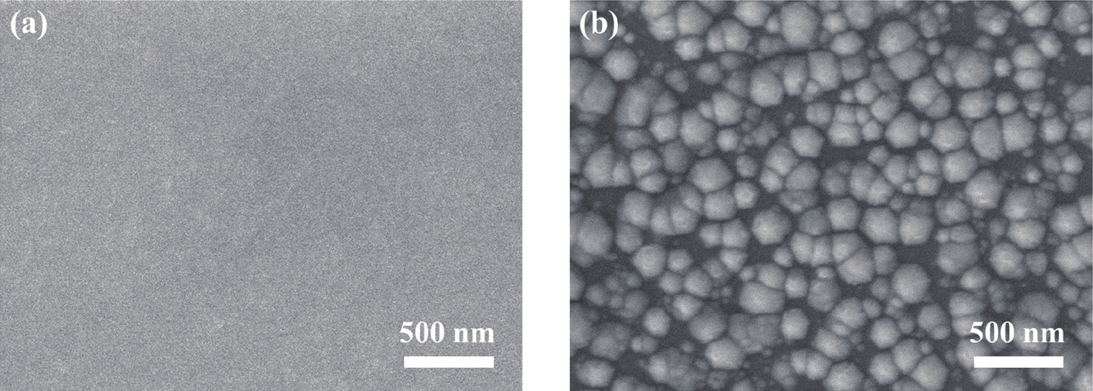
Fig. 1.
Surface SEM images of GaN film (a) before and (b) after KOH etching.
ARTICLES
Nuo Xu, Gaoqiang Deng, Haotian Ma, Shixu Yang, Yunfei Niu, Jiaqi Yu, Yusen Wang, Jingkai Zhao and Yuantao Zhang
Corresponding author: Gaoqiang Deng, denggq@jlu.edu.cn; Yuantao Zhang, zhangyt@jlu.edu.cn
Abstract: A nitrogen-polarity (N-polarity) GaN-based high electron mobility transistor (HEMT) shows great potential for high-frequency solid-state power amplifier applications because its two-dimensional electron gas (2DEG) density and mobility are minimally affected by device scaling. However, the Schottky barrier height (SBH) of N-polarity GaN is low. This leads to a large gate leakage in N-polarity GaN-based HEMTs. In this work, we investigate the effect of annealing on the electrical characteristics of N-polarity GaN-based Schottky barrier diodes (SBDs) with Ni/Au electrodes. Our results show that the annealing time and temperature have a large influence on the electrical properties of N-polarity GaN SBDs. Compared to the N-polarity SBD without annealing, the SBH and rectification ratio at ±5 V of the SBD are increased from 0.51 eV and 30 to 0.77 eV and 7700, respectively, and the ideal factor of the SBD is decreased from 1.66 to 1.54 after an optimized annealing process. Our analysis results suggest that the improvement of the electrical properties of SBDs after annealing is mainly due to the reduction of the interface state density between Schottky contact metals and N-polarity GaN and the increase of barrier height for the electron emission from the trap state at low reverse bias.
Key words: nitrogen polarity, GaN, Schottky barrier diodes, annealing, interface state
| [1] |
Wong M H, Rajan S, Chu R M, et al. N-face high electron mobility transistors with a GaN-spacer. Phys Status Solidi A, 2007, 204, 2049 doi: 10.1002/pssa.200674879
|
| [2] |
Mohanty S, Khan K, Ahmadi E. N-polar GaN: Epitaxy, properties, and device applications. Prog Quant Electron, 2023, 87, 100450 doi: 10.1016/j.pquantelec.2022.100450
|
| [3] |
Mishra U K, Singh J. Semiconductor device physics and design. New York: Springer-Verlag, 2008
|
| [4] |
Wong M H, Keller S, Dasgupta N S, et al. N-polar GaN epitaxy and high electron mobility transistors. Semicond Sci Technol, 2013, 28, 074009 doi: 10.1088/0268-1242/28/7/074009
|
| [5] |
Lu J, Zheng X, Guidry M, et al. Engineering the (In, Al, Ga)N back-barrier to achieve high channel-conductivity for extremely scaled channel-thicknesses in N-polar GaN high-electron-mobility-transistors. Appl Phys Lett, 2014, 104, 092107 doi: 10.1063/1.4867508
|
| [6] |
Diez S, Mohanty S, Kurdak C, et al. Record high electron mobility and low sheet resistance on scaled-channel N-polar GaN/AlN heterostructures grown on on-axis N-polar GaN substrates by plasma-assisted molecular beam epitaxy. Appl Phys Lett, 2020, 117, 042102 doi: 10.1063/5.0014460
|
| [7] |
Wong M H, Pei Y, Palacios T, et al. Low nonalloyed Ohmic contact resistance to nitride high electron mobility transistors using N-face growth. Appl Phys Lett, 2007, 91, 232103 doi: 10.1063/1.2820381
|
| [8] |
Rajan S, Chini A, Wong M H, et al. N-polar GaN/AlGaN/GaN high electron mobility transistors. J Appl Phys, 2007, 102, 044501 doi: 10.1063/1.2769950
|
| [9] |
Brown D F, Williams A, Shinohara K, et al. W-band power performance of AlGaN/GaN DHFETs with regrown n GaN ohmic contacts by MBE. International Electron Devices Meeting, 2011, 19.3. 1 doi: 10.1109/IEDM.2011.6131584
|
| [10] |
Romanczyk B, Wienecke S, Guidry M, et al. Demonstration of constant 8 W/mm power density at 10, 30, and 94 GHz in state-of-the-art millimeter-wave N-polar GaN MISHEMTs. IEEE Trans Electron Devices, 2018, 65, 45 doi: 10.1109/TED.2017.2770087
|
| [11] |
Liu Y, Kauser M Z, Nathan M I, et al. Effects of hydrostatic and uniaxial stress on the Schottky barrier heights of Ga-polarity and N-polarity n-GaN. Appl Phys Lett, 2004, 84, 2112 doi: 10.1063/1.1689392
|
| [12] |
Downey B P, Meyer D J, Katzer D S, et al. Electrical characterization of Schottky contacts to N-polar GaN. Solid State Electron, 2013, 86, 17 doi: 10.1016/j.sse.2013.04.002
|
| [13] |
Suemitsu T, Makabe I. Effective Schottky barrier height model for N-polar and Ga-polar GaN by polarization-induced surface charges with finite thickness. Phys Status Solidi B, 2020, 257, 1900528 doi: 10.1002/pssb.201900528
|
| [14] |
Aoki T, Tanikawa T, Katayama R, et al. Electrical characteristics of N-polar ( $ {000}\bar{{1}} $) p-type GaN Schottky contacts. Jpn J Appl Phys, 2016, 55, 04EJ09 doi: 10.7567/JJAP.55.04EJ09
|
| [15] |
Jang H W, Lee J H, Lee J L. Characterization of band bendings on Ga-face and N-face GaN films grown by metalorganic chemical-vapor deposition. Appl Phys Lett, 2002, 80, 3955 doi: 10.1063/1.1481782
|
| [16] |
Sun Q, Cho Y S, Lee I H, et al. Nitrogen-polar GaN growth evolution on c-plane sapphire. Appl Phys Lett, 2008, 93, 131912 doi: 10.1063/1.2993333
|
| [17] |
Fichtenbaum N A, Mates T E, Keller S, et al. Impurity incorporation in heteroepitaxial N-face and Ga-face GaN films grown by metalorganic chemical vapor deposition. J Cryst Growth, 2008, 310, 1124 doi: 10.1016/j.jcrysgro.2007.12.051
|
| [18] |
Khachariya D, Szymanski D, Breckenridge M H, et al. On the characteristics of N-polar GaN Schottky barrier contacts with LPCVD SiN interlayers. Appl Phys Lett, 2021, 118, 122103 doi: 10.1063/5.0039888
|
| [19] |
Khachariya D, Szymanski D, Reddy P, et al. Schottky contacts to N-polar GaN with SiN interlayer for elevated temperature operation. Appl Phys Lett, 2022, 120, 172109 doi: 10.1063/5.0083588
|
| [20] |
Kim K. Improved conduction in GaN Schottky junctions with HfO2 passivation layers through post-deposition annealing. Jpn J Appl Phys, 2020, 59, 030902 doi: 10.35848/1347-4065/ab71d6
|
| [21] |
Ng H M, Weimann N G, Chowdhury A. GaN nanotip Pyramids formed by anisotropic etching. J Appl Phys, 2003, 94, 650 doi: 10.1063/1.1582233
|
| [22] |
Deng G Q, Zhang Y T, Huang Z, et al. Growth of high quality N-polar n-GaN on vicinal C-face n-SiC substrates for vertical conducting devices. Vacuum, 2016, 130, 119 doi: 10.1016/j.vacuum.2016.05.006
|
| [23] |
Wang Y, Niu Y F, Yu J Q, et al. Growth of high-quality nitrogen-polar GaN film by two-step high-temperature method. Thin Solid Films, 2022, 752, 139246 doi: 10.1016/j.tsf.2022.139246
|
| [24] |
Reddy N N K, Reddy V R, Choi C J. Electrical characteristics and interfacial reactions of rapidly annealed Pt/Ru Schottky contacts on n-type GaN. Phys Status Solidi A, 2011, 208, 1670 doi: 10.1002/pssa.201026748
|
| [25] |
Chen C H, Baier S M, Arch D K, et al. A new and simple model for GaAs heterojunction FET gate characteristics. IEEE Trans Electron Devices, 1988, 35, 570 doi: 10.1109/16.2499
|
| [26] |
Drechsler M, Hofmann D M, Meyer B K, et al. Determination of the conduction band electron effective mass in hexagonal GaN. Jpn J Appl Phys, 1995, 34, L1178 doi: 10.1143/JJAP.34.L1178
|
| [27] |
Qiao D, Yu L S, Lau S S, et al. Dependence of Ni/AlGaN Schottky barrier height on Al mole fraction. J Appl Phys, 2000, 87, 801 doi: 10.1063/1.371944
|
| [28] |
Rhoderick E H, Williams R H. Metal-semiconductor contacts. 2nd ed. Claredon Press, 1988
|
| [29] |
Woo H, Lee J, Jo Y, et al. Barrier lowering and leakage current reduction in Ni-AlGaN/GaN Schottky diodes with an oxygen-treated GaN cap layer. Curr Appl Phys, 2015, 15, 1027 doi: 10.1016/j.cap.2015.06.004
|
| [30] |
Jeon J W, Park S H, Jung S Y, et al. Electrical characteristics of V/Ti/Au contacts to Ga-polar and N-polar n-GaN prepared by different methods. Electrochem Solid-State Lett, 2010, 13, H125 doi: 10.1149/1.3294501
|
| [31] |
Zhang T, Wang Y, Zhang Y N, et al. Comprehensive annealing effects on AlGaN/GaN Schottky barrier diodes with different work-function metals. IEEE Trans Electron Devices, 2021, 68, 2661 doi: 10.1109/TED.2021.3074896
|
| [32] |
Card H C, Rhoderick E H. Studies of tunnel MOS diodes I. Interface effects in silicon Schottky diodes. J Phys D:Appl Phys, 1971, 4, 1589 doi: 10.1088/0022-3727/4/10/319
|
| [33] |
Nagaraju G, Ravindranatha Reddy K, Rajagopal Reddy V. Electrical transport and current properties of rare-earth dysprosium Schottky electrode on p-type GaN at various annealing temperatures. J Semicond, 2017, 38, 114001 doi: 10.1088/1674-4926/38/11/114001
|
| [34] |
Jyothi I, Janardhanam V, Lim Y R, et al. Effect of copper phthalocyanine (CuPc) interlayer on the electrical characteristics of Au/n-GaN Schottky rectifier. Mater Sci Semicond Process, 2015, 30, 420 doi: 10.1016/j.mssp.2014.10.047
|
| [35] |
Tung R T. Electron transport of inhomogeneous Schottky barriers. Appl Phys Lett, 1991, 58, 2821 doi: 10.1063/1.104747
|
| [36] |
Han D P, Ishimoto S, Mano R, et al. Improved reverse leakage current in GaInN-based LEDs with a sputtered AlN buffer layer. IEEE Photonics Technol Lett, 2019, 31, 1971 doi: 10.1109/LPT.2019.2952106
|
| [37] |
Wang Q S, Chen J, Tang H J, et al. Anomalous capacitance in temperature and frequency characteristics of a TiW/ p-InP Schottky barrier diode. Semicond Sci Technol, 2016, 31, 065023 doi: 10.1088/0268-1242/31/6/065023
|
| [38] |
Dong C, Han X X, Li J A, et al. Impacts of growth orientation and N incorporation on the interface-states and the electrical characteristics of Cu/GaAsN Schottky barrier diodes. Phys B, 2017, 527, 52 doi: 10.1016/j.physb.2017.09.125
|
| [39] |
Turuvekere S, Karumuri N, Rahman A A, et al. Gate leakage mechanisms in AlGaN/GaN and AlInN/GaN HEMTs: Comparison and modeling. IEEE Trans Electron Devices, 2013, 60, 3157 doi: 10.1109/TED.2013.2272700
|
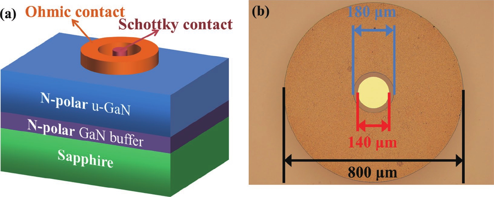
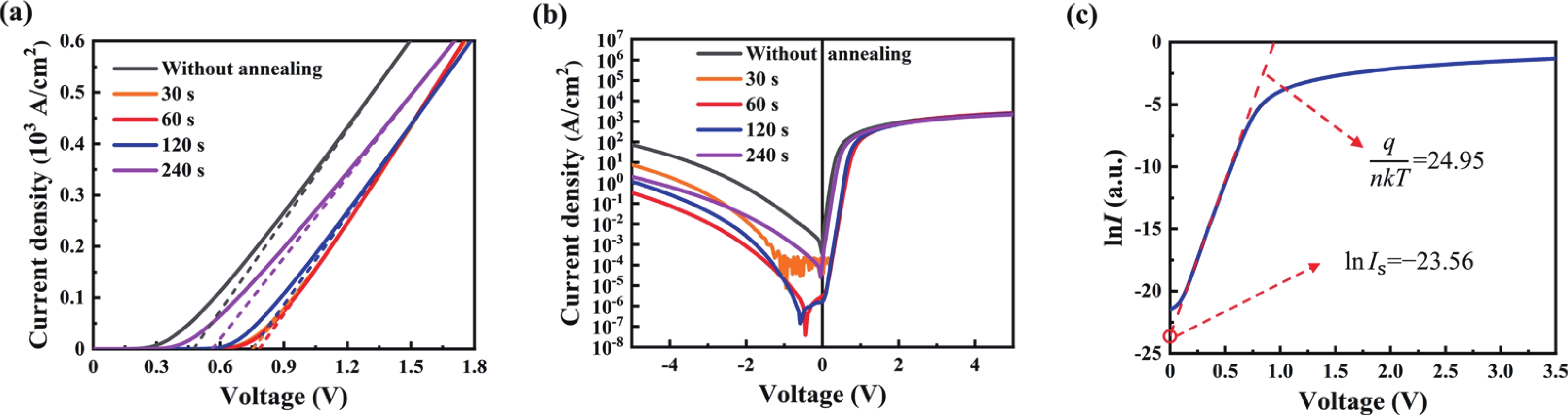
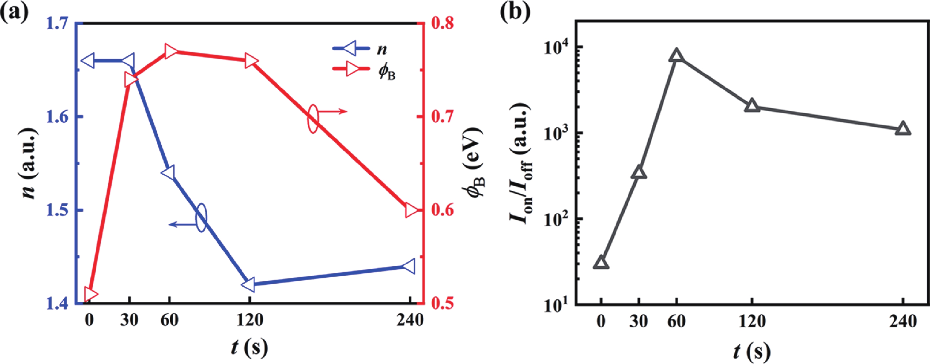
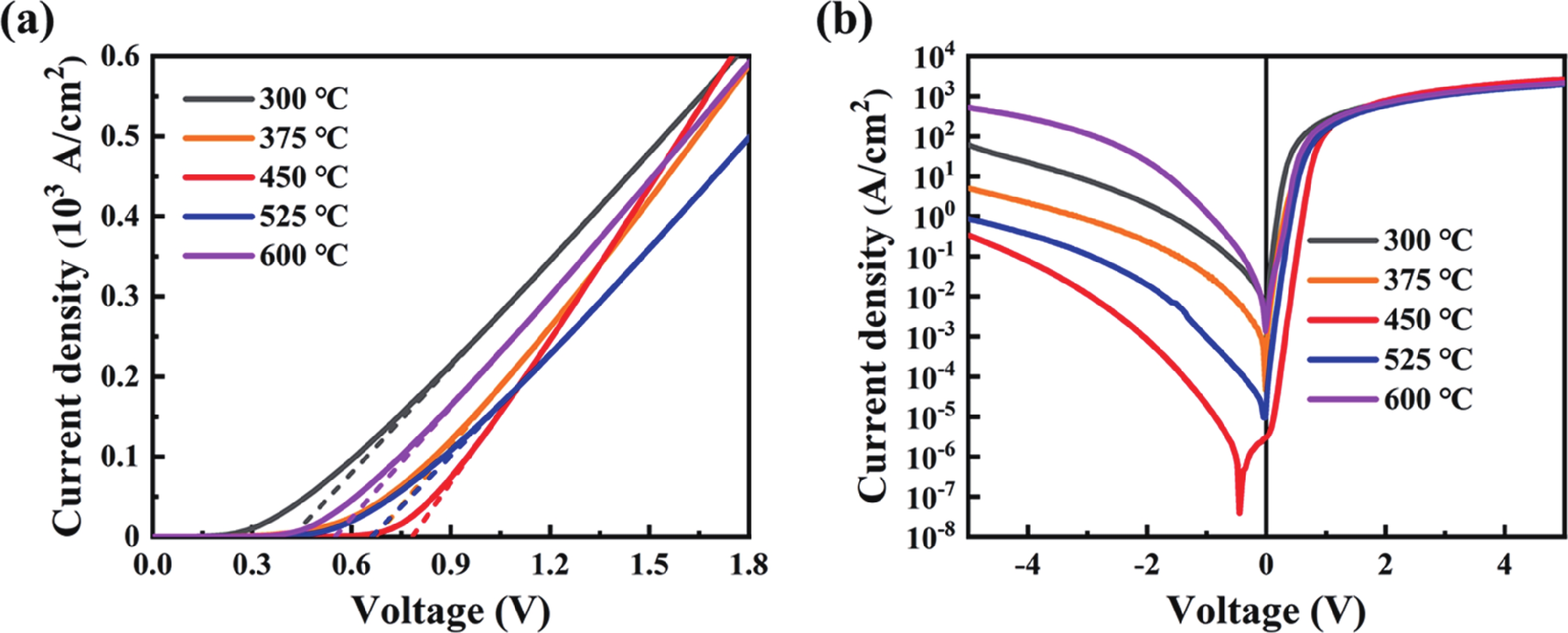
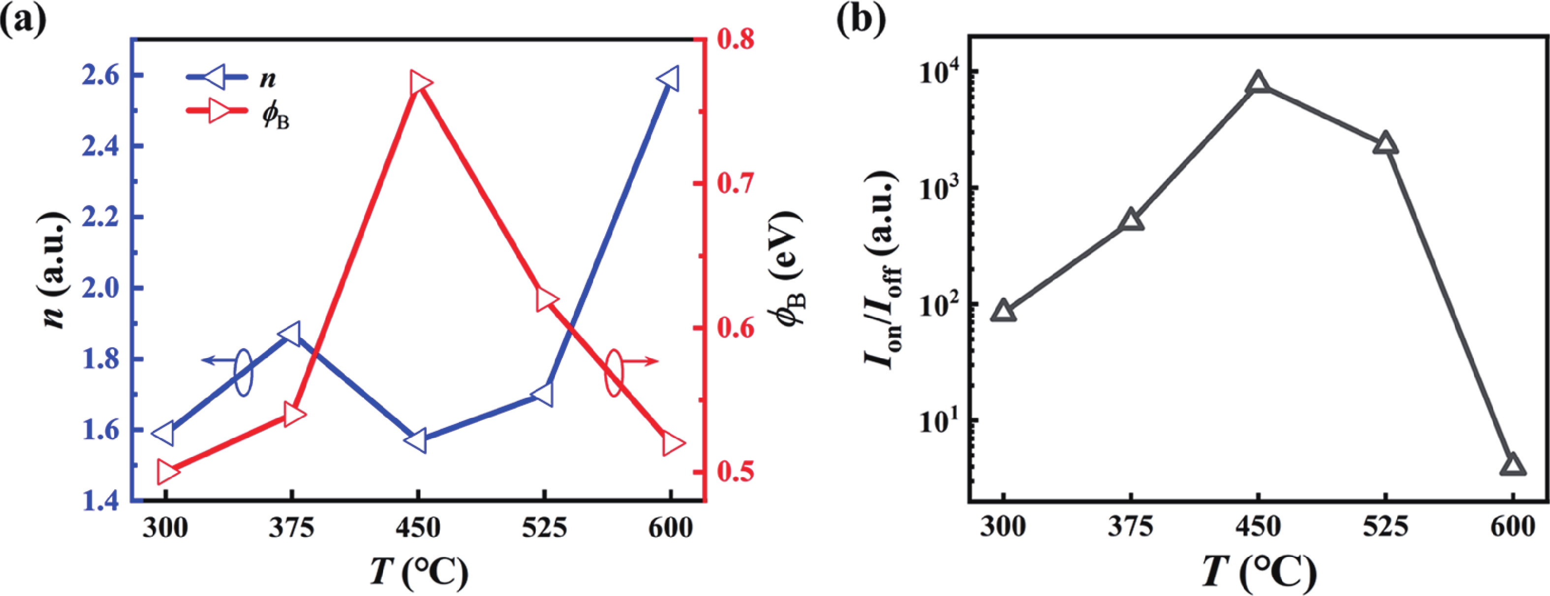
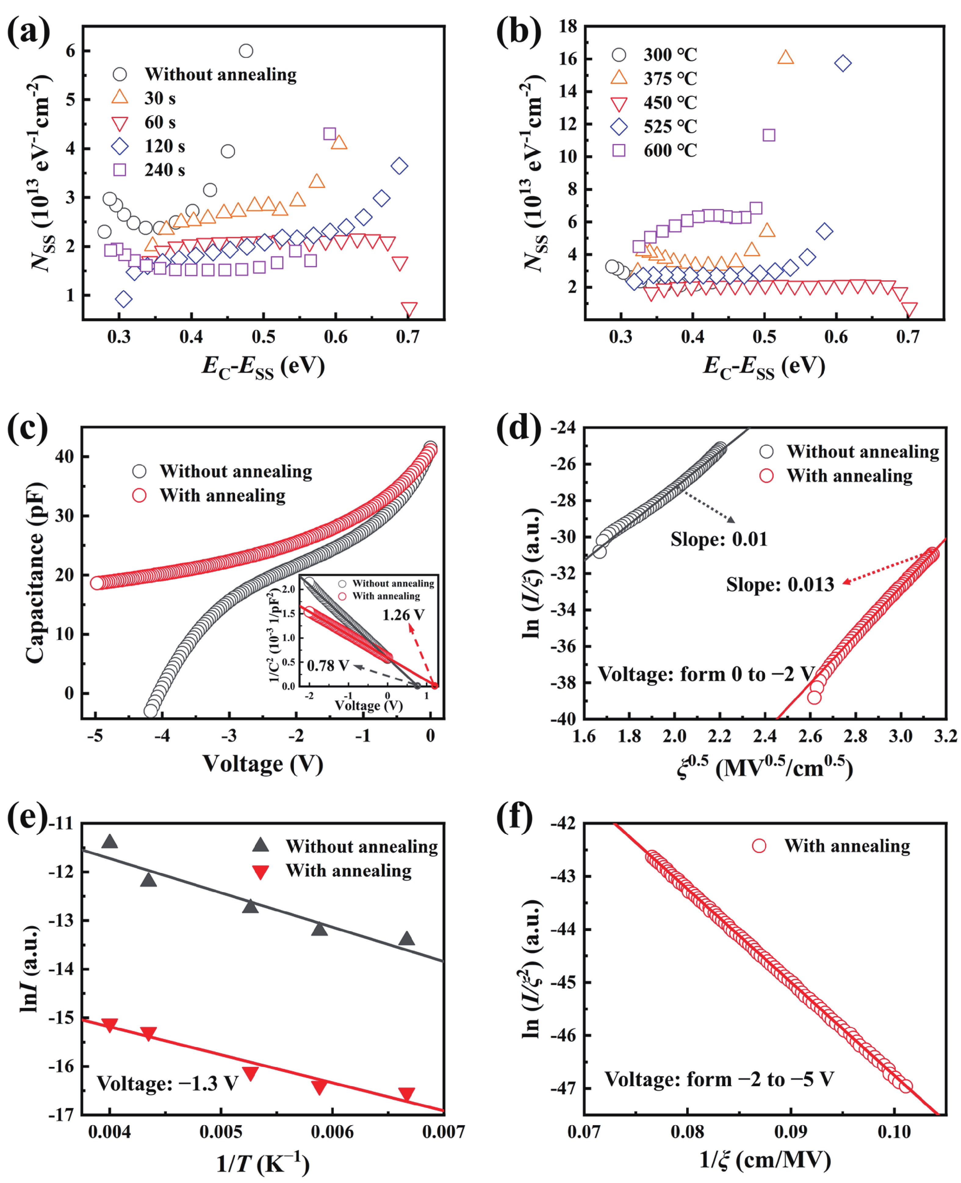
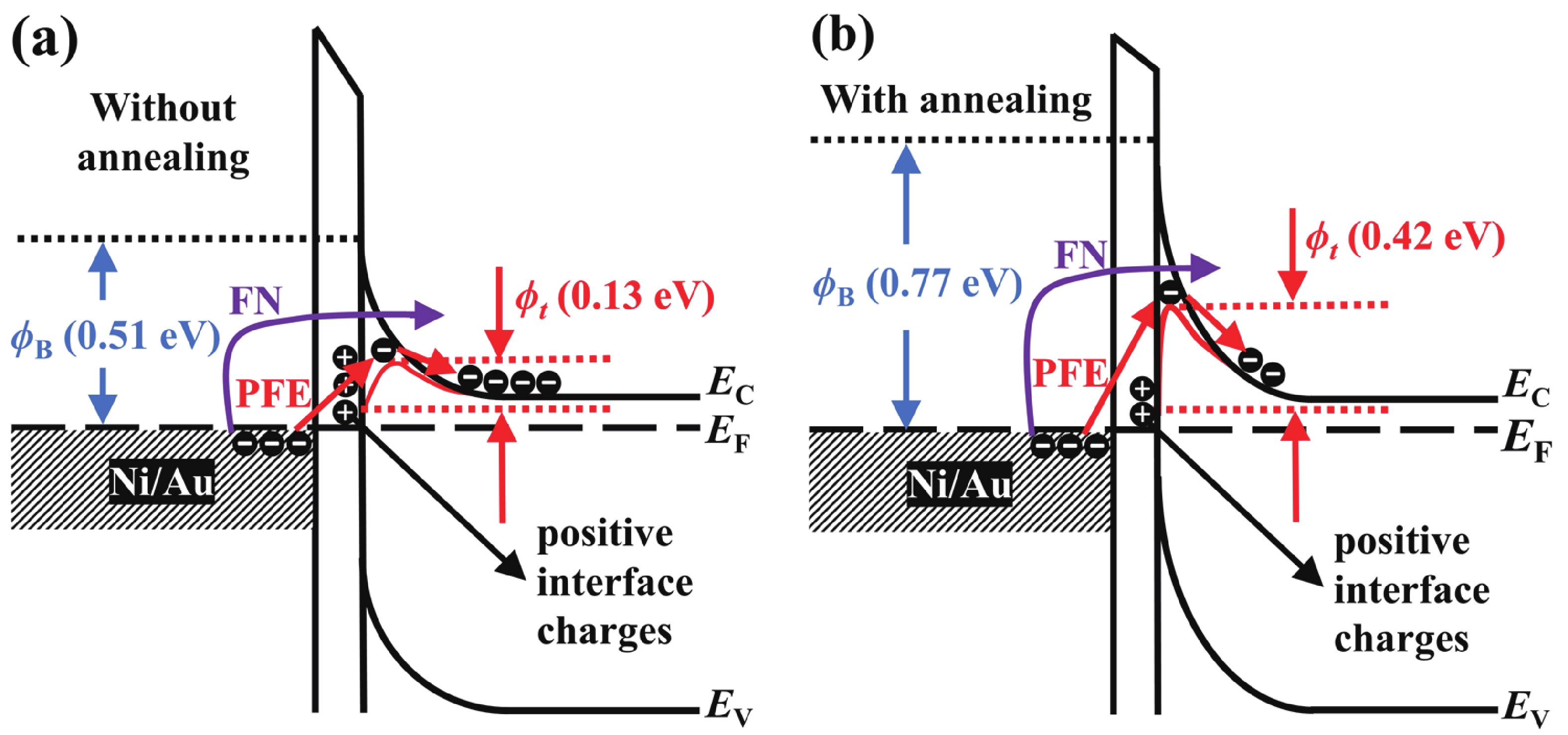
Table 2. Physical notations used in this work and corresponding physical names.
| Physical notations | Physical names | Physical notations | Physical names | Physical notations | Physical names | ||
| ND | Background electron concentration | m* | Electron effective mass of GaN | ESS | Energy of the interface states | ||
| I | Current | m0 | Free electron mass | IPF | Leakage current of Poole−Frenkel emission | ||
| J | Current density | h | Planck's constant | Z | A constant in IPF | ||
| V | Voltage | Ion/Ioff | Rectification ratio | ξ | Electric field | ||
| C | Capacitance | NSS | Density of interface state | $\phi_{\mathrm{t}} $ | Barrier height for the electron emission from the trap state | ||
| Von | Turn-on voltage | εi | Dielectric constant of the thin oxide dielectric layer | εsh | Dielectric constant of GaN at high frequency | ||
| Is | Reverse saturation current | δ | Thickness of the thin oxide dielectric layer | Vbi | Built-in voltage | ||
| q | Absolute value of the electron charge | ε0 | Dielectric constant of vacuum | IFN | Leakage current of Fowler−Nordheim tunneling | ||
| n | Ideal factor | εs | Dielectric constant of GaN | $ {D} $ | A constant in IFN | ||
| k | Boltzmann's constant | WD | Space charge region width on the GaN side | $\phi_{\mathrm{eFN}} $ | Effective Schottky barrier height in IFN | ||
| T | Temperature | NC | Conduction band state density of GaN | EC | Energy of conduction band | ||
| $\phi_{\mathrm{B}} $ | Schottky barrier height | n (V) | Voltage-dependent ideal factor function | EF | Fermi level | ||
| A* | Richard's constant | $\phi_{\mathrm{e}} $ | Effective SBH in n (V) | EV | Energy of valence band |
 DownLoad: CSV
| [1] |
Wong M H, Rajan S, Chu R M, et al. N-face high electron mobility transistors with a GaN-spacer. Phys Status Solidi A, 2007, 204, 2049 doi: 10.1002/pssa.200674879
|
| [2] |
Mohanty S, Khan K, Ahmadi E. N-polar GaN: Epitaxy, properties, and device applications. Prog Quant Electron, 2023, 87, 100450 doi: 10.1016/j.pquantelec.2022.100450
|
| [3] |
Mishra U K, Singh J. Semiconductor device physics and design. New York: Springer-Verlag, 2008
|
| [4] |
Wong M H, Keller S, Dasgupta N S, et al. N-polar GaN epitaxy and high electron mobility transistors. Semicond Sci Technol, 2013, 28, 074009 doi: 10.1088/0268-1242/28/7/074009
|
| [5] |
Lu J, Zheng X, Guidry M, et al. Engineering the (In, Al, Ga)N back-barrier to achieve high channel-conductivity for extremely scaled channel-thicknesses in N-polar GaN high-electron-mobility-transistors. Appl Phys Lett, 2014, 104, 092107 doi: 10.1063/1.4867508
|
| [6] |
Diez S, Mohanty S, Kurdak C, et al. Record high electron mobility and low sheet resistance on scaled-channel N-polar GaN/AlN heterostructures grown on on-axis N-polar GaN substrates by plasma-assisted molecular beam epitaxy. Appl Phys Lett, 2020, 117, 042102 doi: 10.1063/5.0014460
|
| [7] |
Wong M H, Pei Y, Palacios T, et al. Low nonalloyed Ohmic contact resistance to nitride high electron mobility transistors using N-face growth. Appl Phys Lett, 2007, 91, 232103 doi: 10.1063/1.2820381
|
| [8] |
Rajan S, Chini A, Wong M H, et al. N-polar GaN/AlGaN/GaN high electron mobility transistors. J Appl Phys, 2007, 102, 044501 doi: 10.1063/1.2769950
|
| [9] |
Brown D F, Williams A, Shinohara K, et al. W-band power performance of AlGaN/GaN DHFETs with regrown n GaN ohmic contacts by MBE. International Electron Devices Meeting, 2011, 19.3. 1 doi: 10.1109/IEDM.2011.6131584
|
| [10] |
Romanczyk B, Wienecke S, Guidry M, et al. Demonstration of constant 8 W/mm power density at 10, 30, and 94 GHz in state-of-the-art millimeter-wave N-polar GaN MISHEMTs. IEEE Trans Electron Devices, 2018, 65, 45 doi: 10.1109/TED.2017.2770087
|
| [11] |
Liu Y, Kauser M Z, Nathan M I, et al. Effects of hydrostatic and uniaxial stress on the Schottky barrier heights of Ga-polarity and N-polarity n-GaN. Appl Phys Lett, 2004, 84, 2112 doi: 10.1063/1.1689392
|
| [12] |
Downey B P, Meyer D J, Katzer D S, et al. Electrical characterization of Schottky contacts to N-polar GaN. Solid State Electron, 2013, 86, 17 doi: 10.1016/j.sse.2013.04.002
|
| [13] |
Suemitsu T, Makabe I. Effective Schottky barrier height model for N-polar and Ga-polar GaN by polarization-induced surface charges with finite thickness. Phys Status Solidi B, 2020, 257, 1900528 doi: 10.1002/pssb.201900528
|
| [14] |
Aoki T, Tanikawa T, Katayama R, et al. Electrical characteristics of N-polar ( $ {000}\bar{{1}} $) p-type GaN Schottky contacts. Jpn J Appl Phys, 2016, 55, 04EJ09 doi: 10.7567/JJAP.55.04EJ09
|
| [15] |
Jang H W, Lee J H, Lee J L. Characterization of band bendings on Ga-face and N-face GaN films grown by metalorganic chemical-vapor deposition. Appl Phys Lett, 2002, 80, 3955 doi: 10.1063/1.1481782
|
| [16] |
Sun Q, Cho Y S, Lee I H, et al. Nitrogen-polar GaN growth evolution on c-plane sapphire. Appl Phys Lett, 2008, 93, 131912 doi: 10.1063/1.2993333
|
| [17] |
Fichtenbaum N A, Mates T E, Keller S, et al. Impurity incorporation in heteroepitaxial N-face and Ga-face GaN films grown by metalorganic chemical vapor deposition. J Cryst Growth, 2008, 310, 1124 doi: 10.1016/j.jcrysgro.2007.12.051
|
| [18] |
Khachariya D, Szymanski D, Breckenridge M H, et al. On the characteristics of N-polar GaN Schottky barrier contacts with LPCVD SiN interlayers. Appl Phys Lett, 2021, 118, 122103 doi: 10.1063/5.0039888
|
| [19] |
Khachariya D, Szymanski D, Reddy P, et al. Schottky contacts to N-polar GaN with SiN interlayer for elevated temperature operation. Appl Phys Lett, 2022, 120, 172109 doi: 10.1063/5.0083588
|
| [20] |
Kim K. Improved conduction in GaN Schottky junctions with HfO2 passivation layers through post-deposition annealing. Jpn J Appl Phys, 2020, 59, 030902 doi: 10.35848/1347-4065/ab71d6
|
| [21] |
Ng H M, Weimann N G, Chowdhury A. GaN nanotip Pyramids formed by anisotropic etching. J Appl Phys, 2003, 94, 650 doi: 10.1063/1.1582233
|
| [22] |
Deng G Q, Zhang Y T, Huang Z, et al. Growth of high quality N-polar n-GaN on vicinal C-face n-SiC substrates for vertical conducting devices. Vacuum, 2016, 130, 119 doi: 10.1016/j.vacuum.2016.05.006
|
| [23] |
Wang Y, Niu Y F, Yu J Q, et al. Growth of high-quality nitrogen-polar GaN film by two-step high-temperature method. Thin Solid Films, 2022, 752, 139246 doi: 10.1016/j.tsf.2022.139246
|
| [24] |
Reddy N N K, Reddy V R, Choi C J. Electrical characteristics and interfacial reactions of rapidly annealed Pt/Ru Schottky contacts on n-type GaN. Phys Status Solidi A, 2011, 208, 1670 doi: 10.1002/pssa.201026748
|
| [25] |
Chen C H, Baier S M, Arch D K, et al. A new and simple model for GaAs heterojunction FET gate characteristics. IEEE Trans Electron Devices, 1988, 35, 570 doi: 10.1109/16.2499
|
| [26] |
Drechsler M, Hofmann D M, Meyer B K, et al. Determination of the conduction band electron effective mass in hexagonal GaN. Jpn J Appl Phys, 1995, 34, L1178 doi: 10.1143/JJAP.34.L1178
|
| [27] |
Qiao D, Yu L S, Lau S S, et al. Dependence of Ni/AlGaN Schottky barrier height on Al mole fraction. J Appl Phys, 2000, 87, 801 doi: 10.1063/1.371944
|
| [28] |
Rhoderick E H, Williams R H. Metal-semiconductor contacts. 2nd ed. Claredon Press, 1988
|
| [29] |
Woo H, Lee J, Jo Y, et al. Barrier lowering and leakage current reduction in Ni-AlGaN/GaN Schottky diodes with an oxygen-treated GaN cap layer. Curr Appl Phys, 2015, 15, 1027 doi: 10.1016/j.cap.2015.06.004
|
| [30] |
Jeon J W, Park S H, Jung S Y, et al. Electrical characteristics of V/Ti/Au contacts to Ga-polar and N-polar n-GaN prepared by different methods. Electrochem Solid-State Lett, 2010, 13, H125 doi: 10.1149/1.3294501
|
| [31] |
Zhang T, Wang Y, Zhang Y N, et al. Comprehensive annealing effects on AlGaN/GaN Schottky barrier diodes with different work-function metals. IEEE Trans Electron Devices, 2021, 68, 2661 doi: 10.1109/TED.2021.3074896
|
| [32] |
Card H C, Rhoderick E H. Studies of tunnel MOS diodes I. Interface effects in silicon Schottky diodes. J Phys D:Appl Phys, 1971, 4, 1589 doi: 10.1088/0022-3727/4/10/319
|
| [33] |
Nagaraju G, Ravindranatha Reddy K, Rajagopal Reddy V. Electrical transport and current properties of rare-earth dysprosium Schottky electrode on p-type GaN at various annealing temperatures. J Semicond, 2017, 38, 114001 doi: 10.1088/1674-4926/38/11/114001
|
| [34] |
Jyothi I, Janardhanam V, Lim Y R, et al. Effect of copper phthalocyanine (CuPc) interlayer on the electrical characteristics of Au/n-GaN Schottky rectifier. Mater Sci Semicond Process, 2015, 30, 420 doi: 10.1016/j.mssp.2014.10.047
|
| [35] |
Tung R T. Electron transport of inhomogeneous Schottky barriers. Appl Phys Lett, 1991, 58, 2821 doi: 10.1063/1.104747
|
| [36] |
Han D P, Ishimoto S, Mano R, et al. Improved reverse leakage current in GaInN-based LEDs with a sputtered AlN buffer layer. IEEE Photonics Technol Lett, 2019, 31, 1971 doi: 10.1109/LPT.2019.2952106
|
| [37] |
Wang Q S, Chen J, Tang H J, et al. Anomalous capacitance in temperature and frequency characteristics of a TiW/ p-InP Schottky barrier diode. Semicond Sci Technol, 2016, 31, 065023 doi: 10.1088/0268-1242/31/6/065023
|
| [38] |
Dong C, Han X X, Li J A, et al. Impacts of growth orientation and N incorporation on the interface-states and the electrical characteristics of Cu/GaAsN Schottky barrier diodes. Phys B, 2017, 527, 52 doi: 10.1016/j.physb.2017.09.125
|
| [39] |
Turuvekere S, Karumuri N, Rahman A A, et al. Gate leakage mechanisms in AlGaN/GaN and AlInN/GaN HEMTs: Comparison and modeling. IEEE Trans Electron Devices, 2013, 60, 3157 doi: 10.1109/TED.2013.2272700
|


Article views: 501 Times PDF downloads: 92 Times Cited by: 0 Times
Received: 06 September 2023 Revised: 01 December 2023 Online: Accepted Manuscript: 26 December 2023Uncorrected proof: 28 December 2023Published: 10 April 2024
| Citation: |
Nuo Xu, Gaoqiang Deng, Haotian Ma, Shixu Yang, Yunfei Niu, Jiaqi Yu, Yusen Wang, Jingkai Zhao, Yuantao Zhang. Effect of annealing on the electrical performance of N-polarity GaN Schottky barrier diodes[J]. Journal of Semiconductors, 2024, 45(4): 042501. doi: 10.1088/1674-4926/45/4/042501
N Xu, G Q Deng, H T Ma, S X Yang, Y F Niu, J Q Yu, Y S Wang, J K Zhao, Y T Zhang. Effect of annealing on the electrical performance of N-polarity GaN Schottky barrier diodes[J]. J. Semicond, 2024, 45(4): 042501. doi: 10.1088/1674-4926/45/4/042501
Export: BibTex EndNote

|
| [1] |
Wong M H, Rajan S, Chu R M, et al. N-face high electron mobility transistors with a GaN-spacer. Phys Status Solidi A, 2007, 204, 2049 doi: 10.1002/pssa.200674879
|
| [2] |
Mohanty S, Khan K, Ahmadi E. N-polar GaN: Epitaxy, properties, and device applications. Prog Quant Electron, 2023, 87, 100450 doi: 10.1016/j.pquantelec.2022.100450
|
| [3] |
Mishra U K, Singh J. Semiconductor device physics and design. New York: Springer-Verlag, 2008
|
| [4] |
Wong M H, Keller S, Dasgupta N S, et al. N-polar GaN epitaxy and high electron mobility transistors. Semicond Sci Technol, 2013, 28, 074009 doi: 10.1088/0268-1242/28/7/074009
|
| [5] |
Lu J, Zheng X, Guidry M, et al. Engineering the (In, Al, Ga)N back-barrier to achieve high channel-conductivity for extremely scaled channel-thicknesses in N-polar GaN high-electron-mobility-transistors. Appl Phys Lett, 2014, 104, 092107 doi: 10.1063/1.4867508
|
| [6] |
Diez S, Mohanty S, Kurdak C, et al. Record high electron mobility and low sheet resistance on scaled-channel N-polar GaN/AlN heterostructures grown on on-axis N-polar GaN substrates by plasma-assisted molecular beam epitaxy. Appl Phys Lett, 2020, 117, 042102 doi: 10.1063/5.0014460
|
| [7] |
Wong M H, Pei Y, Palacios T, et al. Low nonalloyed Ohmic contact resistance to nitride high electron mobility transistors using N-face growth. Appl Phys Lett, 2007, 91, 232103 doi: 10.1063/1.2820381
|
| [8] |
Rajan S, Chini A, Wong M H, et al. N-polar GaN/AlGaN/GaN high electron mobility transistors. J Appl Phys, 2007, 102, 044501 doi: 10.1063/1.2769950
|
| [9] |
Brown D F, Williams A, Shinohara K, et al. W-band power performance of AlGaN/GaN DHFETs with regrown n GaN ohmic contacts by MBE. International Electron Devices Meeting, 2011, 19.3. 1 doi: 10.1109/IEDM.2011.6131584
|
| [10] |
Romanczyk B, Wienecke S, Guidry M, et al. Demonstration of constant 8 W/mm power density at 10, 30, and 94 GHz in state-of-the-art millimeter-wave N-polar GaN MISHEMTs. IEEE Trans Electron Devices, 2018, 65, 45 doi: 10.1109/TED.2017.2770087
|
| [11] |
Liu Y, Kauser M Z, Nathan M I, et al. Effects of hydrostatic and uniaxial stress on the Schottky barrier heights of Ga-polarity and N-polarity n-GaN. Appl Phys Lett, 2004, 84, 2112 doi: 10.1063/1.1689392
|
| [12] |
Downey B P, Meyer D J, Katzer D S, et al. Electrical characterization of Schottky contacts to N-polar GaN. Solid State Electron, 2013, 86, 17 doi: 10.1016/j.sse.2013.04.002
|
| [13] |
Suemitsu T, Makabe I. Effective Schottky barrier height model for N-polar and Ga-polar GaN by polarization-induced surface charges with finite thickness. Phys Status Solidi B, 2020, 257, 1900528 doi: 10.1002/pssb.201900528
|
| [14] |
Aoki T, Tanikawa T, Katayama R, et al. Electrical characteristics of N-polar ( $ {000}\bar{{1}} $) p-type GaN Schottky contacts. Jpn J Appl Phys, 2016, 55, 04EJ09 doi: 10.7567/JJAP.55.04EJ09
|
| [15] |
Jang H W, Lee J H, Lee J L. Characterization of band bendings on Ga-face and N-face GaN films grown by metalorganic chemical-vapor deposition. Appl Phys Lett, 2002, 80, 3955 doi: 10.1063/1.1481782
|
| [16] |
Sun Q, Cho Y S, Lee I H, et al. Nitrogen-polar GaN growth evolution on c-plane sapphire. Appl Phys Lett, 2008, 93, 131912 doi: 10.1063/1.2993333
|
| [17] |
Fichtenbaum N A, Mates T E, Keller S, et al. Impurity incorporation in heteroepitaxial N-face and Ga-face GaN films grown by metalorganic chemical vapor deposition. J Cryst Growth, 2008, 310, 1124 doi: 10.1016/j.jcrysgro.2007.12.051
|
| [18] |
Khachariya D, Szymanski D, Breckenridge M H, et al. On the characteristics of N-polar GaN Schottky barrier contacts with LPCVD SiN interlayers. Appl Phys Lett, 2021, 118, 122103 doi: 10.1063/5.0039888
|
| [19] |
Khachariya D, Szymanski D, Reddy P, et al. Schottky contacts to N-polar GaN with SiN interlayer for elevated temperature operation. Appl Phys Lett, 2022, 120, 172109 doi: 10.1063/5.0083588
|
| [20] |
Kim K. Improved conduction in GaN Schottky junctions with HfO2 passivation layers through post-deposition annealing. Jpn J Appl Phys, 2020, 59, 030902 doi: 10.35848/1347-4065/ab71d6
|
| [21] |
Ng H M, Weimann N G, Chowdhury A. GaN nanotip Pyramids formed by anisotropic etching. J Appl Phys, 2003, 94, 650 doi: 10.1063/1.1582233
|
| [22] |
Deng G Q, Zhang Y T, Huang Z, et al. Growth of high quality N-polar n-GaN on vicinal C-face n-SiC substrates for vertical conducting devices. Vacuum, 2016, 130, 119 doi: 10.1016/j.vacuum.2016.05.006
|
| [23] |
Wang Y, Niu Y F, Yu J Q, et al. Growth of high-quality nitrogen-polar GaN film by two-step high-temperature method. Thin Solid Films, 2022, 752, 139246 doi: 10.1016/j.tsf.2022.139246
|
| [24] |
Reddy N N K, Reddy V R, Choi C J. Electrical characteristics and interfacial reactions of rapidly annealed Pt/Ru Schottky contacts on n-type GaN. Phys Status Solidi A, 2011, 208, 1670 doi: 10.1002/pssa.201026748
|
| [25] |
Chen C H, Baier S M, Arch D K, et al. A new and simple model for GaAs heterojunction FET gate characteristics. IEEE Trans Electron Devices, 1988, 35, 570 doi: 10.1109/16.2499
|
| [26] |
Drechsler M, Hofmann D M, Meyer B K, et al. Determination of the conduction band electron effective mass in hexagonal GaN. Jpn J Appl Phys, 1995, 34, L1178 doi: 10.1143/JJAP.34.L1178
|
| [27] |
Qiao D, Yu L S, Lau S S, et al. Dependence of Ni/AlGaN Schottky barrier height on Al mole fraction. J Appl Phys, 2000, 87, 801 doi: 10.1063/1.371944
|
| [28] |
Rhoderick E H, Williams R H. Metal-semiconductor contacts. 2nd ed. Claredon Press, 1988
|
| [29] |
Woo H, Lee J, Jo Y, et al. Barrier lowering and leakage current reduction in Ni-AlGaN/GaN Schottky diodes with an oxygen-treated GaN cap layer. Curr Appl Phys, 2015, 15, 1027 doi: 10.1016/j.cap.2015.06.004
|
| [30] |
Jeon J W, Park S H, Jung S Y, et al. Electrical characteristics of V/Ti/Au contacts to Ga-polar and N-polar n-GaN prepared by different methods. Electrochem Solid-State Lett, 2010, 13, H125 doi: 10.1149/1.3294501
|
| [31] |
Zhang T, Wang Y, Zhang Y N, et al. Comprehensive annealing effects on AlGaN/GaN Schottky barrier diodes with different work-function metals. IEEE Trans Electron Devices, 2021, 68, 2661 doi: 10.1109/TED.2021.3074896
|
| [32] |
Card H C, Rhoderick E H. Studies of tunnel MOS diodes I. Interface effects in silicon Schottky diodes. J Phys D:Appl Phys, 1971, 4, 1589 doi: 10.1088/0022-3727/4/10/319
|
| [33] |
Nagaraju G, Ravindranatha Reddy K, Rajagopal Reddy V. Electrical transport and current properties of rare-earth dysprosium Schottky electrode on p-type GaN at various annealing temperatures. J Semicond, 2017, 38, 114001 doi: 10.1088/1674-4926/38/11/114001
|
| [34] |
Jyothi I, Janardhanam V, Lim Y R, et al. Effect of copper phthalocyanine (CuPc) interlayer on the electrical characteristics of Au/n-GaN Schottky rectifier. Mater Sci Semicond Process, 2015, 30, 420 doi: 10.1016/j.mssp.2014.10.047
|
| [35] |
Tung R T. Electron transport of inhomogeneous Schottky barriers. Appl Phys Lett, 1991, 58, 2821 doi: 10.1063/1.104747
|
| [36] |
Han D P, Ishimoto S, Mano R, et al. Improved reverse leakage current in GaInN-based LEDs with a sputtered AlN buffer layer. IEEE Photonics Technol Lett, 2019, 31, 1971 doi: 10.1109/LPT.2019.2952106
|
| [37] |
Wang Q S, Chen J, Tang H J, et al. Anomalous capacitance in temperature and frequency characteristics of a TiW/ p-InP Schottky barrier diode. Semicond Sci Technol, 2016, 31, 065023 doi: 10.1088/0268-1242/31/6/065023
|
| [38] |
Dong C, Han X X, Li J A, et al. Impacts of growth orientation and N incorporation on the interface-states and the electrical characteristics of Cu/GaAsN Schottky barrier diodes. Phys B, 2017, 527, 52 doi: 10.1016/j.physb.2017.09.125
|
| [39] |
Turuvekere S, Karumuri N, Rahman A A, et al. Gate leakage mechanisms in AlGaN/GaN and AlInN/GaN HEMTs: Comparison and modeling. IEEE Trans Electron Devices, 2013, 60, 3157 doi: 10.1109/TED.2013.2272700
|

 WeChat ID
Journal of Semiconductors © 2017 All Rights Reserved 京ICP备05085259号-2


