


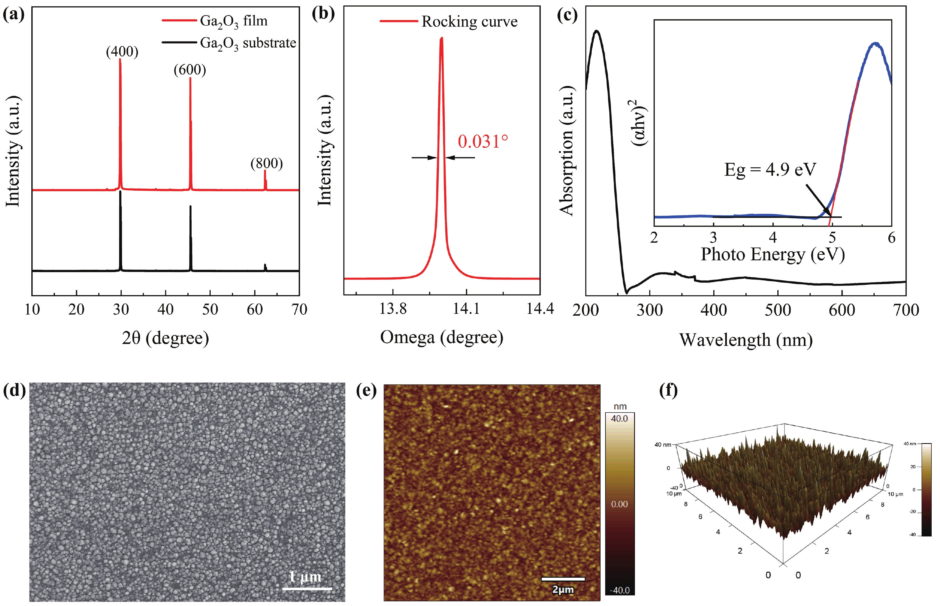
Fig. 1.
(Color online) (a) XRD pattern, (b) rocking curve peak from the (400) plane, (c) absorption spectra, (d) surface SEM image, and the surface AFM of (e) 2D and (f) 3D image of β-Ga2O3 films.
ARTICLES
Xueqiang Ji1, Jinjin Wang1, Song Qi1, Yijie Liang1, Shengrun Hu1, Haochen Zheng1, Sai Zhang1, Jianying Yue1, Xiaohui Qi1, Shan Li2, Zeng Liu2, , Lei Shu3, Weihua Tang2, and Peigang Li1,
Corresponding author: Zeng Liu, zengliu@njupt.edu.cn; Weihua Tang, whtang@njupt.edu.cn; Peigang Li, pgli@bupt.edu.cn
Abstract: The high critical electric field strength of Ga2O3 enables higher operating voltages and reduced switching losses in power electronic devices. Suitable Schottky metals and epitaxial films are essential for further enhancing device performance. In this work, the fabrication of vertical Ga2O3 barrier diodes with three different barrier metals was carried out on an n–-Ga2O3 homogeneous epitaxial film deposited on an n+-β-Ga2O3 substrate by metal−organic chemical vapor deposition, excluding the use of edge terminals. The ideal factor, barrier height, specific on-resistance, and breakdown voltage characteristics of all devices were investigated at room temperature. In addition, the vertical Ga2O3 barrier diodes achieve a higher breakdown voltage and exhibit a reverse leakage as low as 4.82 ×10⁻⁸ A/cm2 by constructing a NiO/Ga2O3 heterojunction. Therefore, Ga2O3 power detailed investigations into Schottky barrier metal and NiO/Ga2O3 heterojunction of Ga2O3 homogeneous epitaxial films are of great research potential in high-efficiency, high-power, and high-reliability applications.
Key words: Ga2O3, Schottky barrier diode, NiO/Ga2O3 heterojunction
| [1] |
Tsao J Y, Chowdhury S, Hollis M A, et al. Ultrawide-bandgap semiconductors: Research opportunities and challenges. Adv Elect Materials, 2018, 4, 1600501 doi: 10.1002/aelm.201600501
|
| [2] |
Jones E A, Wang F F, Costinett D. Review of commercial GaN power devices and GaN-based converter design challenges. IEEE J Emerg Sel Top Power Electron, 2016, 4, 707 doi: 10.1109/JESTPE.2016.2582685
|
| [3] |
Madhusoodhanan S, Sandoval S, Zhao Y, et al. A highly linear temperature sensor using GaN-on-SiC heterojunction diode for high power applications. IEEE Electron Device Lett, 2017, 38, 1105 doi: 10.1109/LED.2017.2714865
|
| [4] |
Millán J, Godignon P, Perpiñà X, et al. A survey of wide bandgap power semiconductor devices. IEEE Trans Power Electron, 2014, 29, 2155 doi: 10.1109/TPEL.2013.2268900
|
| [5] |
Liu Z, Li P G, Zhi Y S, et al. Review of gallium oxide based field-effect transistors and Schottky barrier diodes. Chin Phys B, 2019, 28, 017105 doi: 10.1088/1674-1056/28/1/017105
|
| [6] |
Pearton S J, Ren F, Tadjer M, et al. Perspective: Ga2O3 for ultra-high power rectifiers and MOSFETS. J Appl Phys, 2018, 124, 220901 doi: 10.1063/1.5062841
|
| [7] |
Pearton S J, Yang J C, Cary P H IV, et al. A review of Ga2O3 materials, processing, and devices. Appl Phys Rev, 2018, 5, 011301 doi: 10.1063/1.5006941
|
| [8] |
Higashiwaki M, Sasaki K, Murakami H, et al. Recent progress in Ga2O3 power devices. Semicond Sci Technol, 2016, 31, 034001 doi: 10.1088/0268-1242/31/3/034001
|
| [9] |
Víllora E G, Shimamura K, Yoshikawa Y, et al. Large-size β-Ga2O3 single crystals and wafers. J Cryst Growth, 2004, 270, 420 doi: 10.1016/j.jcrysgro.2004.06.027
|
| [10] |
Xu C X, Shen L Y, Liu H, et al. High-quality β-Ga2O3 films with influence of growth temperature by pulsed laser deposition for solar-blind photodetectors. J Electron Mater, 2021, 50, 2043 doi: 10.1007/s11664-020-08725-3
|
| [11] |
Tadjer M J, Mastro M A, Mahadik N A, et al. Structural, optical, and electrical characterization of monoclinic β-Ga2O3 grown by MOVPE on sapphire substrates. J Electron Mater, 2016, 45, 2031 doi: 10.1007/s11664-016-4346-3
|
| [12] |
Yan Z Y, Li S, Yue J Y, et al. A spiro-MeOTAD/Ga2O3/Si p-i-n junction featuring enhanced self-powered solar-blind sensing via balancing absorption of photons and separation of photogenerated carriers. ACS Appl Mater Interfaces, 2021, 13, 57619 doi: 10.1021/acsami.1c18229
|
| [13] |
Ji X Q, Lu C, Yan Z Y, et al. A review of gallium oxide-based power Schottky barrier diodes. J Phys D Appl Phys, 2022, 55, 443002 doi: 10.1088/1361-6463/ac855c
|
| [14] |
Ren F, Yang J C, Fares C, et al. Device processing and junction formation needs for ultra-high power Ga2O3 electronics. MRS Commun, 2019, 9, 77 doi: 10.1557/mrc.2019.4
|
| [15] |
Dong L P, Zhou S, Pu K W, et al. Electrical contacts in monolayer Ga2O3 field-effect tansistors. Appl Surf Sci, 2021, 564, 150386 doi: 10.1016/j.apsusc.2021.150386
|
| [16] |
Farzana E, Zhang Z, Paul P K, et al. Influence of metal choice on (010) β-Ga2O3 Schottky diode properties. Appl Phys Lett, 2017, 110, 202102 doi: 10.1063/1.4983610
|
| [17] |
Hou C, Gazoni R M, Reeves R J, et al. Oxidized metal Schottky contacts on (010) β-Ga2O3. IEEE Electron Device Lett, 2019, 40, 337 doi: 10.1109/LED.2019.2891304
|
| [18] |
Ingebrigtsen M E, Kuznetsov A Y, Svensson B G, et al. Impact of proton irradiation on conductivity and deep level defects in β-Ga2O3. APL Mater, 2019, 7, 022510 doi: 10.1063/1.5054826
|
| [19] |
Tak B R, Dewan S, Goyal A, et al. Point defects induced work function modulation of β-Ga2O3. Appl Surf Sci, 2019, 465, 973 doi: 10.1016/j.apsusc.2018.09.236
|
| [20] |
Lu X, Deng Y X, Pei Y L, et al. Recent advances in NiO/Ga2O3 heterojunctions for power electronics. J Semicond, 2023, 44, 061802 doi: 10.1088/1674-4926/44/6/061802
|
| [21] |
Li J S, Chiang C C, Xia X Y, et al. Superior high temperature performance of 8 kV NiO/Ga2O3 vertical heterojunction rectifiers. J Mater Chem C, 2023, 11, 7750 doi: 10.1039/D3TC01200J
|
| [22] |
Gong H H, Chen X H, Xu Y, et al. A 1.86-kV double-layered NiO/β-Ga2O3 vertical p–n heterojunction diode. Appl Phys Lett, 2020, 117, 3 doi: 10.1063/5.0010052
|
| [23] |
Luo H X, Zhou X D, Chen Z M, et al. Fabrication and characterization of high-voltage NiO/β-Ga2O3 heterojunction power diodes. IEEE Trans Electron Devices, 2021, 68, 3991 doi: 10.1109/TED.2021.3091548
|
| [24] |
He Q M, Mu W X, Dong H, et al. Schottky barrier diode based on β-Ga2O3 (100) single crystal substrate and its temperature-dependent electrical characteristics. Appl Phys Lett, 2017, 110, 093503 doi: 10.1063/1.4977766
|
| [25] |
Anhar Uddin Bhuiyan A F M, Feng Z X, Johnson J M, et al. MOCVD epitaxy of ultrawide bandgap β-(AlxGa1–x)2O3 with high-Al composition on (100) β-Ga2O3 substrates. Cryst Growth Des, 2020, 20, 6722 doi: 10.1021/acs.cgd.0c00864
|
| [26] |
Alema F, Hertog B, Osinsky A, et al. Fast growth rate of epitaxial β-Ga2O3 by close coupled showerhead MOCVD. J Cryst Growth, 2017, 475, 77 doi: 10.1016/j.jcrysgro.2017.06.001
|
| [27] |
Cui W, Guo D Y, Zhao X L, et al. Solar-blind photodetector based on Ga2O3 nanowires array film growth from inserted Al2O3 ultrathin interlayers for improving responsivity. RSC Adv, 2016, 6, 100683 doi: 10.1039/C6RA16108A
|
| [28] |
Wei H L, Chen Z W, Wu Z P, et al. Epitaxial growth and characterization of CuGa2O4 films by laser molecular beam epitaxy. AIP Adv, 2017, 7, 115216 doi: 10.1063/1.5009032
|
| [29] |
Ji X Q, Yue J Y, Qi X H, et al. Homoepitaxial Si-doped Gallium Oxide films by MOCVD with tunable electron concentrations and electrical properties. Vacuum, 2023, 210, 111902 doi: 10.1016/j.vacuum.2023.111902
|
| [30] |
Yakimov E B, Polyakov A Y, Shchemerov I V, et al. Photosensitivity of Ga2O3 Schottky diodes: Effects of deep acceptor traps present before and after neutron irradiation. APL Mater, 2020, 8, 2 doi: 10.1063/5.0030105
|
| [31] |
Shen Y X, Feng Q, Zhang K, et al. The investigation of temperature dependent electrical characteristics of Au/Ni/β-(InGa)2O3 Schottky diode. Superlattices Microstruct, 2019, 133, 106179 doi: 10.1016/j.spmi.2019.106179
|
| [32] |
Oh S, Yang G, Kim J. Electrical characteristics of vertical Ni/β-Ga2O3 Schottky barrier diodes at high temperatures. ECS J Solid State Sci Technol, 2016, 6, Q3022 doi: 10.1149/2.0041702jss
|
| [33] |
Luan S Z, Dong L P, Ma X F, et al. The further investigation of N-doped β-Ga2O3 thin films with native defects for Schottky-barrier diode. J Alloys Compd, 2020, 812, 152026 doi: 10.1016/j.jallcom.2019.152026
|
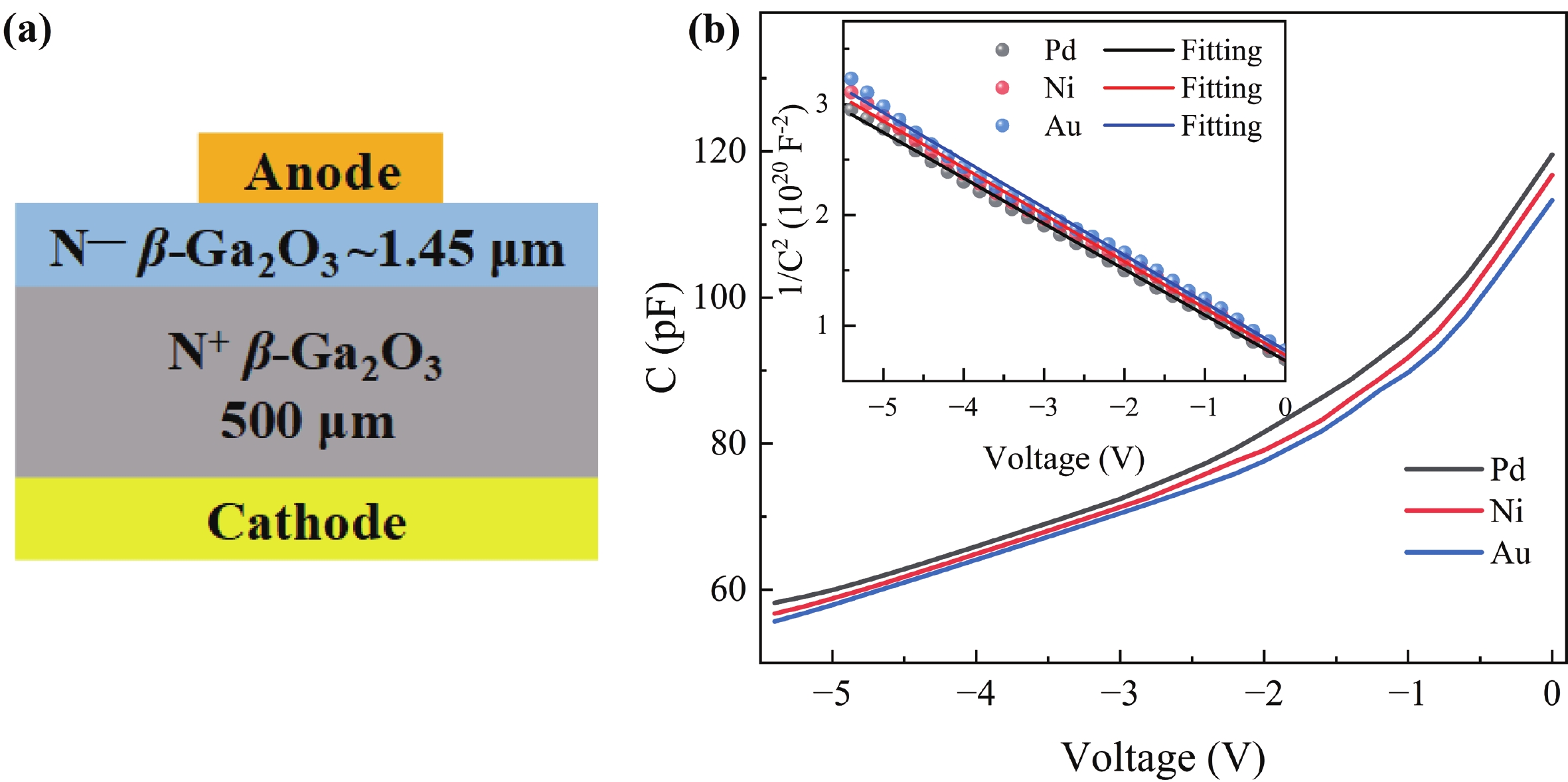
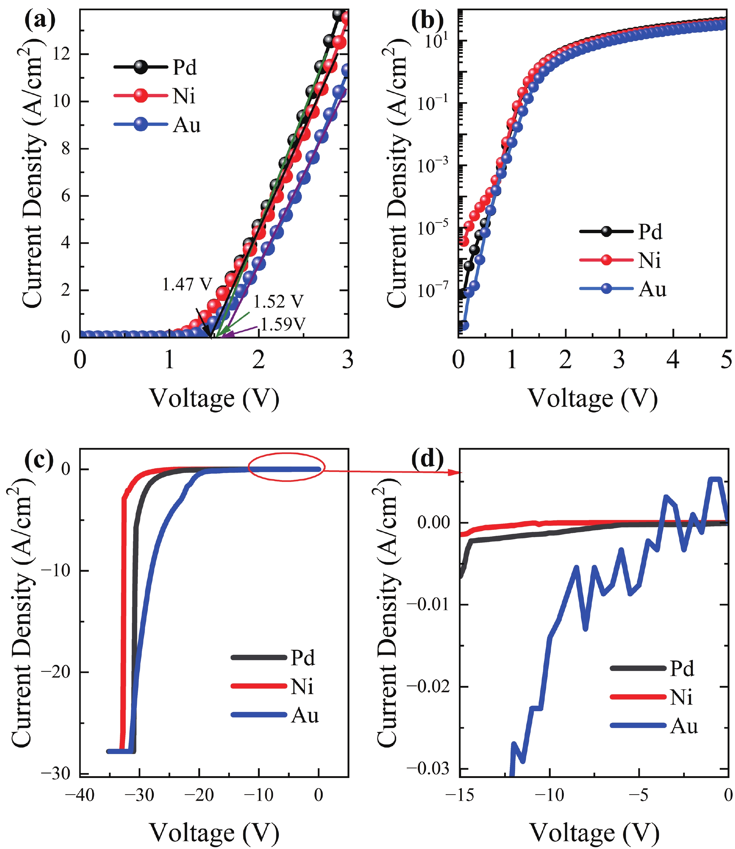
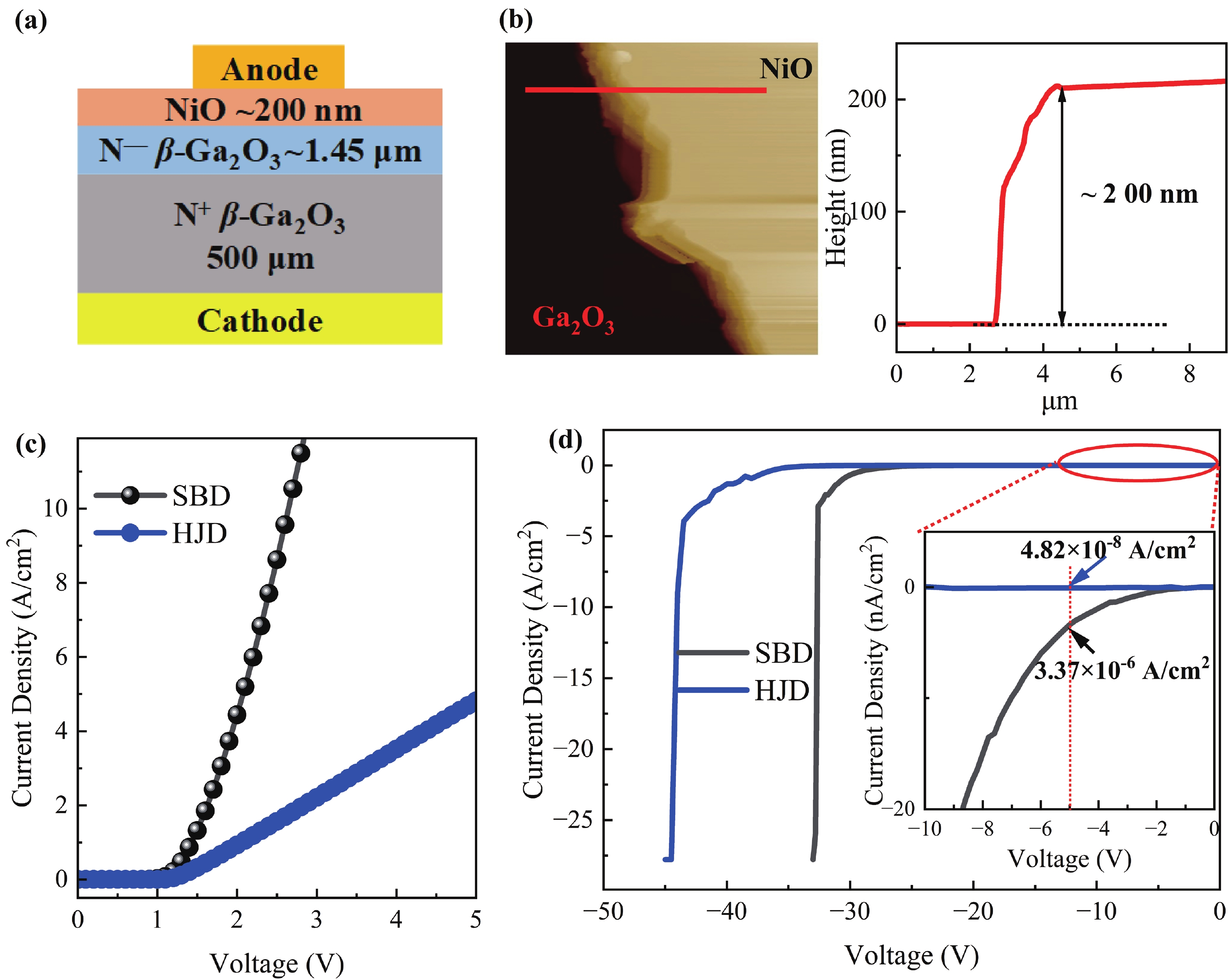

Table 1. The summary of electrical performances for β-Ga2O3 SBDs and HJDs.
| Devices | n | ΦJ−V (eV) | Vbi (V) | Ron (Ω·cm2) | Vbr (V) |
| β-Ga2O3 SBDs: Au | 3.9 | 0.67 | 1.59 | 0.12 | 31.5 |
| β-Ga2O3 SBDs: Pd | 3.0 | 0.70 | 1.52 | 0.09 | 30.8 |
| β-Ga2O3 SBDs: Ni | 3.5 | 0.56 | 1.47 | 0.11 | 33 |
 DownLoad: CSV
| [1] |
Tsao J Y, Chowdhury S, Hollis M A, et al. Ultrawide-bandgap semiconductors: Research opportunities and challenges. Adv Elect Materials, 2018, 4, 1600501 doi: 10.1002/aelm.201600501
|
| [2] |
Jones E A, Wang F F, Costinett D. Review of commercial GaN power devices and GaN-based converter design challenges. IEEE J Emerg Sel Top Power Electron, 2016, 4, 707 doi: 10.1109/JESTPE.2016.2582685
|
| [3] |
Madhusoodhanan S, Sandoval S, Zhao Y, et al. A highly linear temperature sensor using GaN-on-SiC heterojunction diode for high power applications. IEEE Electron Device Lett, 2017, 38, 1105 doi: 10.1109/LED.2017.2714865
|
| [4] |
Millán J, Godignon P, Perpiñà X, et al. A survey of wide bandgap power semiconductor devices. IEEE Trans Power Electron, 2014, 29, 2155 doi: 10.1109/TPEL.2013.2268900
|
| [5] |
Liu Z, Li P G, Zhi Y S, et al. Review of gallium oxide based field-effect transistors and Schottky barrier diodes. Chin Phys B, 2019, 28, 017105 doi: 10.1088/1674-1056/28/1/017105
|
| [6] |
Pearton S J, Ren F, Tadjer M, et al. Perspective: Ga2O3 for ultra-high power rectifiers and MOSFETS. J Appl Phys, 2018, 124, 220901 doi: 10.1063/1.5062841
|
| [7] |
Pearton S J, Yang J C, Cary P H IV, et al. A review of Ga2O3 materials, processing, and devices. Appl Phys Rev, 2018, 5, 011301 doi: 10.1063/1.5006941
|
| [8] |
Higashiwaki M, Sasaki K, Murakami H, et al. Recent progress in Ga2O3 power devices. Semicond Sci Technol, 2016, 31, 034001 doi: 10.1088/0268-1242/31/3/034001
|
| [9] |
Víllora E G, Shimamura K, Yoshikawa Y, et al. Large-size β-Ga2O3 single crystals and wafers. J Cryst Growth, 2004, 270, 420 doi: 10.1016/j.jcrysgro.2004.06.027
|
| [10] |
Xu C X, Shen L Y, Liu H, et al. High-quality β-Ga2O3 films with influence of growth temperature by pulsed laser deposition for solar-blind photodetectors. J Electron Mater, 2021, 50, 2043 doi: 10.1007/s11664-020-08725-3
|
| [11] |
Tadjer M J, Mastro M A, Mahadik N A, et al. Structural, optical, and electrical characterization of monoclinic β-Ga2O3 grown by MOVPE on sapphire substrates. J Electron Mater, 2016, 45, 2031 doi: 10.1007/s11664-016-4346-3
|
| [12] |
Yan Z Y, Li S, Yue J Y, et al. A spiro-MeOTAD/Ga2O3/Si p-i-n junction featuring enhanced self-powered solar-blind sensing via balancing absorption of photons and separation of photogenerated carriers. ACS Appl Mater Interfaces, 2021, 13, 57619 doi: 10.1021/acsami.1c18229
|
| [13] |
Ji X Q, Lu C, Yan Z Y, et al. A review of gallium oxide-based power Schottky barrier diodes. J Phys D Appl Phys, 2022, 55, 443002 doi: 10.1088/1361-6463/ac855c
|
| [14] |
Ren F, Yang J C, Fares C, et al. Device processing and junction formation needs for ultra-high power Ga2O3 electronics. MRS Commun, 2019, 9, 77 doi: 10.1557/mrc.2019.4
|
| [15] |
Dong L P, Zhou S, Pu K W, et al. Electrical contacts in monolayer Ga2O3 field-effect tansistors. Appl Surf Sci, 2021, 564, 150386 doi: 10.1016/j.apsusc.2021.150386
|
| [16] |
Farzana E, Zhang Z, Paul P K, et al. Influence of metal choice on (010) β-Ga2O3 Schottky diode properties. Appl Phys Lett, 2017, 110, 202102 doi: 10.1063/1.4983610
|
| [17] |
Hou C, Gazoni R M, Reeves R J, et al. Oxidized metal Schottky contacts on (010) β-Ga2O3. IEEE Electron Device Lett, 2019, 40, 337 doi: 10.1109/LED.2019.2891304
|
| [18] |
Ingebrigtsen M E, Kuznetsov A Y, Svensson B G, et al. Impact of proton irradiation on conductivity and deep level defects in β-Ga2O3. APL Mater, 2019, 7, 022510 doi: 10.1063/1.5054826
|
| [19] |
Tak B R, Dewan S, Goyal A, et al. Point defects induced work function modulation of β-Ga2O3. Appl Surf Sci, 2019, 465, 973 doi: 10.1016/j.apsusc.2018.09.236
|
| [20] |
Lu X, Deng Y X, Pei Y L, et al. Recent advances in NiO/Ga2O3 heterojunctions for power electronics. J Semicond, 2023, 44, 061802 doi: 10.1088/1674-4926/44/6/061802
|
| [21] |
Li J S, Chiang C C, Xia X Y, et al. Superior high temperature performance of 8 kV NiO/Ga2O3 vertical heterojunction rectifiers. J Mater Chem C, 2023, 11, 7750 doi: 10.1039/D3TC01200J
|
| [22] |
Gong H H, Chen X H, Xu Y, et al. A 1.86-kV double-layered NiO/β-Ga2O3 vertical p–n heterojunction diode. Appl Phys Lett, 2020, 117, 3 doi: 10.1063/5.0010052
|
| [23] |
Luo H X, Zhou X D, Chen Z M, et al. Fabrication and characterization of high-voltage NiO/β-Ga2O3 heterojunction power diodes. IEEE Trans Electron Devices, 2021, 68, 3991 doi: 10.1109/TED.2021.3091548
|
| [24] |
He Q M, Mu W X, Dong H, et al. Schottky barrier diode based on β-Ga2O3 (100) single crystal substrate and its temperature-dependent electrical characteristics. Appl Phys Lett, 2017, 110, 093503 doi: 10.1063/1.4977766
|
| [25] |
Anhar Uddin Bhuiyan A F M, Feng Z X, Johnson J M, et al. MOCVD epitaxy of ultrawide bandgap β-(AlxGa1–x)2O3 with high-Al composition on (100) β-Ga2O3 substrates. Cryst Growth Des, 2020, 20, 6722 doi: 10.1021/acs.cgd.0c00864
|
| [26] |
Alema F, Hertog B, Osinsky A, et al. Fast growth rate of epitaxial β-Ga2O3 by close coupled showerhead MOCVD. J Cryst Growth, 2017, 475, 77 doi: 10.1016/j.jcrysgro.2017.06.001
|
| [27] |
Cui W, Guo D Y, Zhao X L, et al. Solar-blind photodetector based on Ga2O3 nanowires array film growth from inserted Al2O3 ultrathin interlayers for improving responsivity. RSC Adv, 2016, 6, 100683 doi: 10.1039/C6RA16108A
|
| [28] |
Wei H L, Chen Z W, Wu Z P, et al. Epitaxial growth and characterization of CuGa2O4 films by laser molecular beam epitaxy. AIP Adv, 2017, 7, 115216 doi: 10.1063/1.5009032
|
| [29] |
Ji X Q, Yue J Y, Qi X H, et al. Homoepitaxial Si-doped Gallium Oxide films by MOCVD with tunable electron concentrations and electrical properties. Vacuum, 2023, 210, 111902 doi: 10.1016/j.vacuum.2023.111902
|
| [30] |
Yakimov E B, Polyakov A Y, Shchemerov I V, et al. Photosensitivity of Ga2O3 Schottky diodes: Effects of deep acceptor traps present before and after neutron irradiation. APL Mater, 2020, 8, 2 doi: 10.1063/5.0030105
|
| [31] |
Shen Y X, Feng Q, Zhang K, et al. The investigation of temperature dependent electrical characteristics of Au/Ni/β-(InGa)2O3 Schottky diode. Superlattices Microstruct, 2019, 133, 106179 doi: 10.1016/j.spmi.2019.106179
|
| [32] |
Oh S, Yang G, Kim J. Electrical characteristics of vertical Ni/β-Ga2O3 Schottky barrier diodes at high temperatures. ECS J Solid State Sci Technol, 2016, 6, Q3022 doi: 10.1149/2.0041702jss
|
| [33] |
Luan S Z, Dong L P, Ma X F, et al. The further investigation of N-doped β-Ga2O3 thin films with native defects for Schottky-barrier diode. J Alloys Compd, 2020, 812, 152026 doi: 10.1016/j.jallcom.2019.152026
|


Article views: 557 Times PDF downloads: 90 Times Cited by: 0 Times
Received: 21 September 2023 Revised: 27 November 2023 Online: Accepted Manuscript: 13 January 2024Uncorrected proof: 22 February 2024Published: 10 April 2024
| Citation: |
Xueqiang Ji, Jinjin Wang, Song Qi, Yijie Liang, Shengrun Hu, Haochen Zheng, Sai Zhang, Jianying Yue, Xiaohui Qi, Shan Li, Zeng Liu, Lei Shu, Weihua Tang, Peigang Li. Improvement of Ga2O3 vertical Schottky barrier diode by constructing NiO/Ga2O3 heterojunction[J]. Journal of Semiconductors, 2024, 45(4): 042503. doi: 10.1088/1674-4926/45/4/042503
X Q Ji, J J Wang, S Qi, Y J Liang, S R Hu, H C Zheng, S Zhang, J Y Yue, X H Qi, S Li, Z Liu, L Shu, W H Tang, P G Li. Improvement of Ga2O3 vertical Schottky barrier diode by constructing NiO/Ga2O3 heterojunction[J]. J. Semicond, 2024, 45(4): 042503. doi: 10.1088/1674-4926/45/4/042503
Export: BibTex EndNote

|
| [1] |
Tsao J Y, Chowdhury S, Hollis M A, et al. Ultrawide-bandgap semiconductors: Research opportunities and challenges. Adv Elect Materials, 2018, 4, 1600501 doi: 10.1002/aelm.201600501
|
| [2] |
Jones E A, Wang F F, Costinett D. Review of commercial GaN power devices and GaN-based converter design challenges. IEEE J Emerg Sel Top Power Electron, 2016, 4, 707 doi: 10.1109/JESTPE.2016.2582685
|
| [3] |
Madhusoodhanan S, Sandoval S, Zhao Y, et al. A highly linear temperature sensor using GaN-on-SiC heterojunction diode for high power applications. IEEE Electron Device Lett, 2017, 38, 1105 doi: 10.1109/LED.2017.2714865
|
| [4] |
Millán J, Godignon P, Perpiñà X, et al. A survey of wide bandgap power semiconductor devices. IEEE Trans Power Electron, 2014, 29, 2155 doi: 10.1109/TPEL.2013.2268900
|
| [5] |
Liu Z, Li P G, Zhi Y S, et al. Review of gallium oxide based field-effect transistors and Schottky barrier diodes. Chin Phys B, 2019, 28, 017105 doi: 10.1088/1674-1056/28/1/017105
|
| [6] |
Pearton S J, Ren F, Tadjer M, et al. Perspective: Ga2O3 for ultra-high power rectifiers and MOSFETS. J Appl Phys, 2018, 124, 220901 doi: 10.1063/1.5062841
|
| [7] |
Pearton S J, Yang J C, Cary P H IV, et al. A review of Ga2O3 materials, processing, and devices. Appl Phys Rev, 2018, 5, 011301 doi: 10.1063/1.5006941
|
| [8] |
Higashiwaki M, Sasaki K, Murakami H, et al. Recent progress in Ga2O3 power devices. Semicond Sci Technol, 2016, 31, 034001 doi: 10.1088/0268-1242/31/3/034001
|
| [9] |
Víllora E G, Shimamura K, Yoshikawa Y, et al. Large-size β-Ga2O3 single crystals and wafers. J Cryst Growth, 2004, 270, 420 doi: 10.1016/j.jcrysgro.2004.06.027
|
| [10] |
Xu C X, Shen L Y, Liu H, et al. High-quality β-Ga2O3 films with influence of growth temperature by pulsed laser deposition for solar-blind photodetectors. J Electron Mater, 2021, 50, 2043 doi: 10.1007/s11664-020-08725-3
|
| [11] |
Tadjer M J, Mastro M A, Mahadik N A, et al. Structural, optical, and electrical characterization of monoclinic β-Ga2O3 grown by MOVPE on sapphire substrates. J Electron Mater, 2016, 45, 2031 doi: 10.1007/s11664-016-4346-3
|
| [12] |
Yan Z Y, Li S, Yue J Y, et al. A spiro-MeOTAD/Ga2O3/Si p-i-n junction featuring enhanced self-powered solar-blind sensing via balancing absorption of photons and separation of photogenerated carriers. ACS Appl Mater Interfaces, 2021, 13, 57619 doi: 10.1021/acsami.1c18229
|
| [13] |
Ji X Q, Lu C, Yan Z Y, et al. A review of gallium oxide-based power Schottky barrier diodes. J Phys D Appl Phys, 2022, 55, 443002 doi: 10.1088/1361-6463/ac855c
|
| [14] |
Ren F, Yang J C, Fares C, et al. Device processing and junction formation needs for ultra-high power Ga2O3 electronics. MRS Commun, 2019, 9, 77 doi: 10.1557/mrc.2019.4
|
| [15] |
Dong L P, Zhou S, Pu K W, et al. Electrical contacts in monolayer Ga2O3 field-effect tansistors. Appl Surf Sci, 2021, 564, 150386 doi: 10.1016/j.apsusc.2021.150386
|
| [16] |
Farzana E, Zhang Z, Paul P K, et al. Influence of metal choice on (010) β-Ga2O3 Schottky diode properties. Appl Phys Lett, 2017, 110, 202102 doi: 10.1063/1.4983610
|
| [17] |
Hou C, Gazoni R M, Reeves R J, et al. Oxidized metal Schottky contacts on (010) β-Ga2O3. IEEE Electron Device Lett, 2019, 40, 337 doi: 10.1109/LED.2019.2891304
|
| [18] |
Ingebrigtsen M E, Kuznetsov A Y, Svensson B G, et al. Impact of proton irradiation on conductivity and deep level defects in β-Ga2O3. APL Mater, 2019, 7, 022510 doi: 10.1063/1.5054826
|
| [19] |
Tak B R, Dewan S, Goyal A, et al. Point defects induced work function modulation of β-Ga2O3. Appl Surf Sci, 2019, 465, 973 doi: 10.1016/j.apsusc.2018.09.236
|
| [20] |
Lu X, Deng Y X, Pei Y L, et al. Recent advances in NiO/Ga2O3 heterojunctions for power electronics. J Semicond, 2023, 44, 061802 doi: 10.1088/1674-4926/44/6/061802
|
| [21] |
Li J S, Chiang C C, Xia X Y, et al. Superior high temperature performance of 8 kV NiO/Ga2O3 vertical heterojunction rectifiers. J Mater Chem C, 2023, 11, 7750 doi: 10.1039/D3TC01200J
|
| [22] |
Gong H H, Chen X H, Xu Y, et al. A 1.86-kV double-layered NiO/β-Ga2O3 vertical p–n heterojunction diode. Appl Phys Lett, 2020, 117, 3 doi: 10.1063/5.0010052
|
| [23] |
Luo H X, Zhou X D, Chen Z M, et al. Fabrication and characterization of high-voltage NiO/β-Ga2O3 heterojunction power diodes. IEEE Trans Electron Devices, 2021, 68, 3991 doi: 10.1109/TED.2021.3091548
|
| [24] |
He Q M, Mu W X, Dong H, et al. Schottky barrier diode based on β-Ga2O3 (100) single crystal substrate and its temperature-dependent electrical characteristics. Appl Phys Lett, 2017, 110, 093503 doi: 10.1063/1.4977766
|
| [25] |
Anhar Uddin Bhuiyan A F M, Feng Z X, Johnson J M, et al. MOCVD epitaxy of ultrawide bandgap β-(AlxGa1–x)2O3 with high-Al composition on (100) β-Ga2O3 substrates. Cryst Growth Des, 2020, 20, 6722 doi: 10.1021/acs.cgd.0c00864
|
| [26] |
Alema F, Hertog B, Osinsky A, et al. Fast growth rate of epitaxial β-Ga2O3 by close coupled showerhead MOCVD. J Cryst Growth, 2017, 475, 77 doi: 10.1016/j.jcrysgro.2017.06.001
|
| [27] |
Cui W, Guo D Y, Zhao X L, et al. Solar-blind photodetector based on Ga2O3 nanowires array film growth from inserted Al2O3 ultrathin interlayers for improving responsivity. RSC Adv, 2016, 6, 100683 doi: 10.1039/C6RA16108A
|
| [28] |
Wei H L, Chen Z W, Wu Z P, et al. Epitaxial growth and characterization of CuGa2O4 films by laser molecular beam epitaxy. AIP Adv, 2017, 7, 115216 doi: 10.1063/1.5009032
|
| [29] |
Ji X Q, Yue J Y, Qi X H, et al. Homoepitaxial Si-doped Gallium Oxide films by MOCVD with tunable electron concentrations and electrical properties. Vacuum, 2023, 210, 111902 doi: 10.1016/j.vacuum.2023.111902
|
| [30] |
Yakimov E B, Polyakov A Y, Shchemerov I V, et al. Photosensitivity of Ga2O3 Schottky diodes: Effects of deep acceptor traps present before and after neutron irradiation. APL Mater, 2020, 8, 2 doi: 10.1063/5.0030105
|
| [31] |
Shen Y X, Feng Q, Zhang K, et al. The investigation of temperature dependent electrical characteristics of Au/Ni/β-(InGa)2O3 Schottky diode. Superlattices Microstruct, 2019, 133, 106179 doi: 10.1016/j.spmi.2019.106179
|
| [32] |
Oh S, Yang G, Kim J. Electrical characteristics of vertical Ni/β-Ga2O3 Schottky barrier diodes at high temperatures. ECS J Solid State Sci Technol, 2016, 6, Q3022 doi: 10.1149/2.0041702jss
|
| [33] |
Luan S Z, Dong L P, Ma X F, et al. The further investigation of N-doped β-Ga2O3 thin films with native defects for Schottky-barrier diode. J Alloys Compd, 2020, 812, 152026 doi: 10.1016/j.jallcom.2019.152026
|

 WeChat ID
Journal of Semiconductors © 2017 All Rights Reserved 京ICP备05085259号-2


