


Fig. 1.
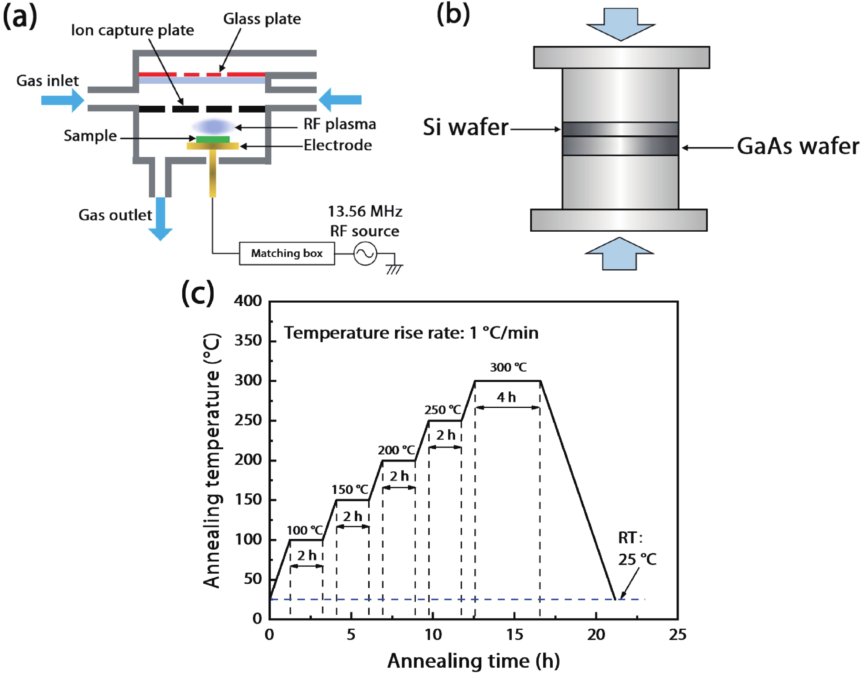
(Color online) (a) Schematic diagram of the plasma-activated wafer; (b) GaAs and Si wafer bonding; (c) time-dependent curve of annealing temperature at an annealing temperature of 300 ℃.
ARTICLES
Rui Huang1, , Zhiyong Wang2, Kai Wu1, Hao Xu1, Qing Wang1 and Yecai Guo1
Corresponding author: Rui Huang, ruihuang@cwxu.edu.cn
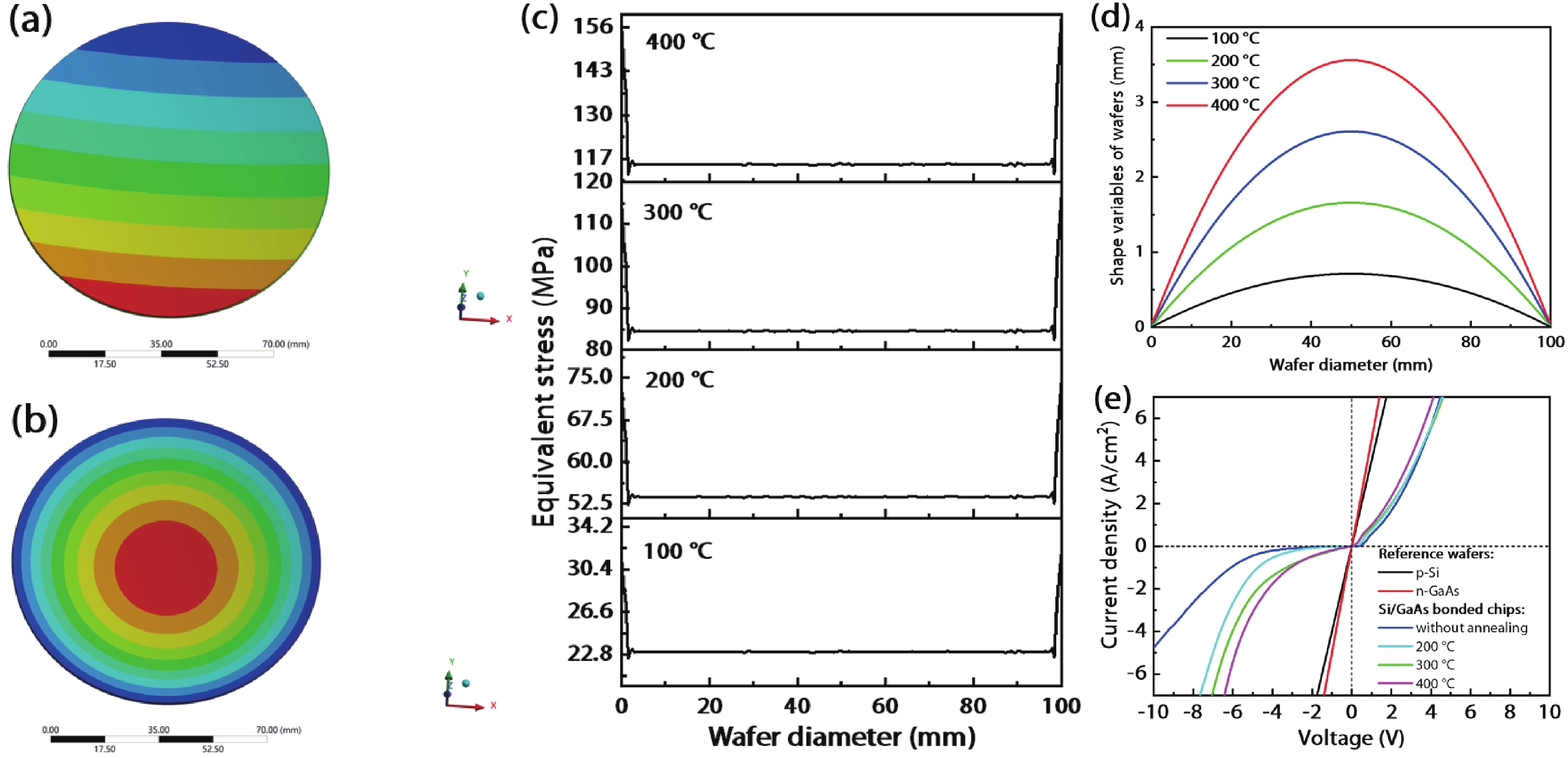
Abstract: High-quality bonding of 4-inch GaAs and Si is achieved using plasma-activated bonding technology. The influence of Ar plasma activation on surface morphology is discussed. When the annealing temperature is 300 ℃, the bonding strength reaches a maximum of 6.2 MPa. In addition, a thermal stress model for GaAs/Si wafers is established based on finite element analysis to obtain the distribution of equivalent stress and deformation variables at different temperatures. The shape variation of the wafer is directly proportional to the annealing temperature. At an annealing temperature of 400 ℃, the maximum protrusion of 4 inches GaAs/Si wafers is 3.6 mm. The interface of GaAs/Si wafers is observed to be dense and defect-free using a transmission electron microscope. The characterization of interface elements by X-ray energy dispersion spectroscopy indicates that the elements at the interface undergo mutual diffusion, which is beneficial for improving the bonding strength of the interface. There is an amorphous transition layer with a thickness of about 5 nm at the bonding interface. The preparation of Si-based GaAs heterojunctions can enrich the types of materials required for the development of integrated circuits, improve the performance of materials and devices, and promote the development of microelectronics technology.
Key words: plasma-activated bonding, bonding strength, thermal stress model, mutual diffusion
| [1] |
Atabaki A H, Moazeni S, Pavanello F, et al. Integrating photonics with silicon nanoelectronics for the next generation of systems on a chip. Nature, 2018, 556, 349 doi: 10.1038/s41586-018-0028-z
|
| [2] |
Lu Y, Alvarez A, Kao C H, et al. An electronic silicon-based memristor with a high switching uniformity. Nat Electron, 2019, 2, 66 doi: 10.1038/s41928-019-0204-7
|
| [3] |
Yoshikawa K, Kawasaki H, Yoshida W, et al. Silicon heterojunction solar cell with interdigitated back contacts for a photoconversion efficiency over 26%. Nat Energy, 2017, 2, 17032 doi: 10.1038/nenergy.2017.32
|
| [4] |
Morimoto M, Nishida S, Shigekawa N, et al. Surface-activating-bonding-based low-resistance Si/III-V junctions. Electron Lett, 2013, 49, 830 doi: 10.1049/el.2013.1553
|
| [5] |
Theis T N, Wong H S P. The end of Moore’s law: A new beginning for information technology. Comput Sci Eng, 2017, 19, 41 doi: 10.1109/MCSE.2017.29
|
| [6] |
Huang Y Y, Zhang L Y, Jing R Y, et al. Superior piezoelectric performance with high operating temperature in bismuth ferrite-based ternary ceramics. J Mater Sci Technol, 2024, 169, 172 doi: 10.1016/j.jmst.2023.05.063
|
| [7] |
Su R X, Fu S L, Lu Z T, et al. Over GHz bandwidth SAW filter based on 32° Y-X LN/SiO2/poly-Si/Si heterostructure with multilayer electrode modulation. Appl Phys Lett, 2022, 120, 253501 doi: 10.1063/5.0092767
|
| [8] |
Bai C, Kim M. Single power-conversion active-clamped AC/DC converter employing Si/SiC hybrid switch. IEEE Trans Ind Electron, 2024, 71, 1616 doi: 10.1109/TIE.2023.3262889
|
| [9] |
Hager A, Güniat L, Morgan N, et al. The implementation of thermal and UV nanoimprint lithography for selective area epitaxy. Nanotechnology, 2023, 34, 445301
|
| [10] |
Lin T, Xie J N, Ning S H, et al. Study on the p-type ohmic contact in GaAs-based laser diode. Mater Sci Semicond Process, 2021, 124, 105622 doi: 10.1016/j.mssp.2020.105622
|
| [11] |
Yu J H, Xu M K, Liang L Y, et al. Separative extended-gate AlGaAs/GaAs HEMT biosensors based on capacitance change strategy. Appl Phys Lett, 2020, 116, 123704 doi: 10.1063/5.0001786
|
| [12] |
Kim S, Geum D M, Park M S, et al. Fabrication of high-quality GaAs-based photodetector arrays on Si. Appl Phys Lett, 2017, 110, 153505 doi: 10.1063/1.4980122
|
| [13] |
Schindler P C, Korn D, Stamatiadis C, et al. Monolithic GaAs electro-optic IQ modulator demonstrated at 150 gbit/s with 64QAM. J Light Technol, 2014, 32, 760 doi: 10.1109/JLT.2013.2278381
|
| [14] |
Shigekawa N, Kozono R, Yoon S, et al. Effects of post bonding annealing on GaAs//Si bonding interfaces and its application for sacrificial-layer-etching based multijunction solar cells. Sol Energy Mater Sol Cells, 2020, 210, 110501 doi: 10.1016/j.solmat.2020.110501
|
| [15] |
Cheng C W, Shiu K T, Li N, et al. Epitaxial lift-off process for gallium arsenide substrate reuse and flexible electronics. Nat Commun, 2013, 4, 1577 doi: 10.1038/ncomms2583
|
| [16] |
Ohno Y, Liang J B, Shigekawa N, et al. Chemical bonding at room temperature via surface activation to fabricate low-resistance GaAs/Si heterointerfaces. Appl Surf Sci, 2020, 525, 146610 doi: 10.1016/j.apsusc.2020.146610
|
| [17] |
Yamajo S, Yoon S, Liang J B, et al. Hard X-ray photoelectron spectroscopy investigation of annealing effects on buried oxide in GaAs/Si junctions by surface-activated bonding. Appl Surf Sci, 2019, 473, 627 doi: 10.1016/j.apsusc.2018.12.199
|
| [18] |
Shen Y J, Wang Y Z, Yang Y, et al. Influence of surface roughness and hydrophilicity on bonding strength of concrete-rock interface. Constr Build Mater, 2019, 213, 156 doi: 10.1016/j.conbuildmat.2019.04.078
|
| [19] |
He G R, Yang G H, Zheng W H, et al. Analysis of Si/GaAs Bonding Stresses with the Finite Element Method. J Semicond, 2006, 27, 11
|
| [20] |
Zhao Y Q, Liu W, Bao Y D, et al. Plasma-activated GaAs/Si wafer bonding with high mechanical strength and electrical conductivity. Mater Sci Semicond Process, 2022, 143, 106481 doi: 10.1016/j.mssp.2022.106481
|


Article views: 553 Times PDF downloads: 41 Times Cited by: 0 Times
Received: 29 September 2023 Revised: 29 November 2023 Online: Accepted Manuscript: 02 January 2024Uncorrected proof: 03 January 2024Published: 10 April 2024
| Citation: |
Rui Huang, Zhiyong Wang, Kai Wu, Hao Xu, Qing Wang, Yecai Guo. Hybrid bonding of GaAs and Si wafers at low temperature by Ar plasma activation[J]. Journal of Semiconductors, 2024, 45(4): 042701. doi: 10.1088/1674-4926/45/4/042701
R Huang, Z Y Wang, K Wu, H Xu, Q Wang, Y C Guo. Hybrid bonding of GaAs and Si wafers at low temperature by Ar plasma activation[J]. J. Semicond, 2024, 45(4): 042701. doi: 10.1088/1674-4926/45/4/042701
Export: BibTex EndNote

|
| [1] |
Atabaki A H, Moazeni S, Pavanello F, et al. Integrating photonics with silicon nanoelectronics for the next generation of systems on a chip. Nature, 2018, 556, 349 doi: 10.1038/s41586-018-0028-z
|
| [2] |
Lu Y, Alvarez A, Kao C H, et al. An electronic silicon-based memristor with a high switching uniformity. Nat Electron, 2019, 2, 66 doi: 10.1038/s41928-019-0204-7
|
| [3] |
Yoshikawa K, Kawasaki H, Yoshida W, et al. Silicon heterojunction solar cell with interdigitated back contacts for a photoconversion efficiency over 26%. Nat Energy, 2017, 2, 17032 doi: 10.1038/nenergy.2017.32
|
| [4] |
Morimoto M, Nishida S, Shigekawa N, et al. Surface-activating-bonding-based low-resistance Si/III-V junctions. Electron Lett, 2013, 49, 830 doi: 10.1049/el.2013.1553
|
| [5] |
Theis T N, Wong H S P. The end of Moore’s law: A new beginning for information technology. Comput Sci Eng, 2017, 19, 41 doi: 10.1109/MCSE.2017.29
|
| [6] |
Huang Y Y, Zhang L Y, Jing R Y, et al. Superior piezoelectric performance with high operating temperature in bismuth ferrite-based ternary ceramics. J Mater Sci Technol, 2024, 169, 172 doi: 10.1016/j.jmst.2023.05.063
|
| [7] |
Su R X, Fu S L, Lu Z T, et al. Over GHz bandwidth SAW filter based on 32° Y-X LN/SiO2/poly-Si/Si heterostructure with multilayer electrode modulation. Appl Phys Lett, 2022, 120, 253501 doi: 10.1063/5.0092767
|
| [8] |
Bai C, Kim M. Single power-conversion active-clamped AC/DC converter employing Si/SiC hybrid switch. IEEE Trans Ind Electron, 2024, 71, 1616 doi: 10.1109/TIE.2023.3262889
|
| [9] |
Hager A, Güniat L, Morgan N, et al. The implementation of thermal and UV nanoimprint lithography for selective area epitaxy. Nanotechnology, 2023, 34, 445301
|
| [10] |
Lin T, Xie J N, Ning S H, et al. Study on the p-type ohmic contact in GaAs-based laser diode. Mater Sci Semicond Process, 2021, 124, 105622 doi: 10.1016/j.mssp.2020.105622
|
| [11] |
Yu J H, Xu M K, Liang L Y, et al. Separative extended-gate AlGaAs/GaAs HEMT biosensors based on capacitance change strategy. Appl Phys Lett, 2020, 116, 123704 doi: 10.1063/5.0001786
|
| [12] |
Kim S, Geum D M, Park M S, et al. Fabrication of high-quality GaAs-based photodetector arrays on Si. Appl Phys Lett, 2017, 110, 153505 doi: 10.1063/1.4980122
|
| [13] |
Schindler P C, Korn D, Stamatiadis C, et al. Monolithic GaAs electro-optic IQ modulator demonstrated at 150 gbit/s with 64QAM. J Light Technol, 2014, 32, 760 doi: 10.1109/JLT.2013.2278381
|
| [14] |
Shigekawa N, Kozono R, Yoon S, et al. Effects of post bonding annealing on GaAs//Si bonding interfaces and its application for sacrificial-layer-etching based multijunction solar cells. Sol Energy Mater Sol Cells, 2020, 210, 110501 doi: 10.1016/j.solmat.2020.110501
|
| [15] |
Cheng C W, Shiu K T, Li N, et al. Epitaxial lift-off process for gallium arsenide substrate reuse and flexible electronics. Nat Commun, 2013, 4, 1577 doi: 10.1038/ncomms2583
|
| [16] |
Ohno Y, Liang J B, Shigekawa N, et al. Chemical bonding at room temperature via surface activation to fabricate low-resistance GaAs/Si heterointerfaces. Appl Surf Sci, 2020, 525, 146610 doi: 10.1016/j.apsusc.2020.146610
|
| [17] |
Yamajo S, Yoon S, Liang J B, et al. Hard X-ray photoelectron spectroscopy investigation of annealing effects on buried oxide in GaAs/Si junctions by surface-activated bonding. Appl Surf Sci, 2019, 473, 627 doi: 10.1016/j.apsusc.2018.12.199
|
| [18] |
Shen Y J, Wang Y Z, Yang Y, et al. Influence of surface roughness and hydrophilicity on bonding strength of concrete-rock interface. Constr Build Mater, 2019, 213, 156 doi: 10.1016/j.conbuildmat.2019.04.078
|
| [19] |
He G R, Yang G H, Zheng W H, et al. Analysis of Si/GaAs Bonding Stresses with the Finite Element Method. J Semicond, 2006, 27, 11
|
| [20] |
Zhao Y Q, Liu W, Bao Y D, et al. Plasma-activated GaAs/Si wafer bonding with high mechanical strength and electrical conductivity. Mater Sci Semicond Process, 2022, 143, 106481 doi: 10.1016/j.mssp.2022.106481
|

 WeChat ID
Journal of Semiconductors © 2017 All Rights Reserved 京ICP备05085259号-2

 DownLoad:

