| [1] |
Liu W Z, Liu Y J, Yang Z Q, et al. Flexible solar cells based on foldable silicon wafers with blunted edges. Nature, 2023, 617, 717 doi: 10.1038/s41586-023-05921-z |
| [2] |
Wu X M, Gao C S, Chen Q Z, et al. High-performance vertical field-effect organic photovoltaics. Nat Commun, 2023, 14, 1579 doi: 10.1038/s41467-023-37174-9 |
| [3] |
Chu X B, Ye Q F, Wang Z H, et al. Surface in situ reconstruction of inorganic perovskite films enabling long carrier lifetimes and solar cells with 21% efficiency. Nat Energy, 2023, 8, 372 doi: 10.1038/s41560-023-01220-z |
| [4] |
Yang T H, Gao L L, Lu J, et al. One-stone-for-two-birds strategy to attain beyond 25% perovskite solar cells. Nat Commun, 2023, 14, 839 doi: 10.1038/s41467-023-36229-1 |
| [5] |
Ji R, Zhang Z B, Hofstetter Y J, et al. Perovskite phase heterojunction solar cells. Nat Energy, 2022, 7, 1170 doi: 10.1038/s41560-022-01154-y |
| [6] |
Polman A, Knight M, Garnett E C, et al. Photovoltaic materials: Present efficiencies and future challenges. Science, 2016, 352, aad4424 doi: 10.1126/science.aad4424 |
| [7] |
Kublitski J, Hofacker A, Boroujeni B K, et al. Reverse dark current in organic photodetectors and the major role of traps as source of noise. Nat Commun, 2021, 12, 551 doi: 10.1038/s41467-020-20856-z |
| [8] |
Sakhatskyi K, Turedi B, Matt G J, et al. Stable perovskite single-crystal X-ray imaging detectors with single-photon sensitivity. Nat Photonics, 2023, 17, 510 doi: 10.1038/s41566-023-01207-y |
| [9] |
Sun Y, Xu S T, Xu Z Q, et al. Mesoscopic sliding ferroelectricity enabled photovoltaic random access memory for material-level artificial vision system. Nat Commun, 2022, 13, 5391 doi: 10.1038/s41467-022-33118-x |
| [10] |
Pi L J, Wang P F, Liang S J, et al. Broadband convolutional processing using band-alignment-tunable heterostructures. Nat Electron, 2022, 5, 248 doi: 10.1038/s41928-022-00747-5 |
| [11] |
Liu K L, Jin B, Han W, et al. A wafer-scale van der Waals dielectric made from an inorganic molecular crystal film. Nat Electron, 2021, 4, 906 doi: 10.1038/s41928-021-00683-w |
| [12] |
Liu Y, Huang Y, Duan X F. Van der Waals integration before and beyond two-dimensional materials. Nature, 2019, 567, 323 doi: 10.1038/s41586-019-1013-x |
| [13] |
Jariwala D, Marks T J, Hersam M C. Mixed-dimensional van der Waals heterostructures. Nat Mater, 2017, 16, 170 doi: 10.1038/nmat4703 |
| [14] |
Shu Z W, Peng Q J, Huang P, et al. Growth of ultrathin ternary teallite (PbSnS 2) flakes for highly anisotropic optoelectronics. Matter, 2020, 2, 977 doi: 10.1016/j.matt.2020.01.013 |
| [15] |
Liang S J, Cheng B, Cui X Y, et al. Van der Waals heterostructures for high-performance device applications: Challenges and opportunities. Adv Mater, 2020, 32, 1903800 doi: 10.1002/adma.201903800 |
| [16] |
Xu Y S, Liu T, Liu K L, et al. Scalable integration of hybrid high-κ dielectric materials on two-dimensional semiconductors. Nat Mater, 2023, 22, 1078 doi: 10.1038/s41563-023-01626-w |
| [17] |
Britnell L, Ribeiro R M, Eckmann A, et al. Strong light-matter interactions in heterostructures of atomically thin films. Science, 2013, 340, 1311 doi: 10.1126/science.1235547 |
| [18] |
Lukman S, Ding L, Xu L, et al. High oscillator strength interlayer excitons in two-dimensional heterostructures for mid-infrared photodetection. Nat Nanotechnol, 2020, 15, 675 doi: 10.1038/s41565-020-0717-2 |
| [19] |
Zhang Y J, Ideue T, Onga M, et al. Enhanced intrinsic photovoltaic effect in tungsten disulfide nanotubes. Nature, 2019, 570, 349 doi: 10.1038/s41586-019-1303-3 |
| [20] |
Chen Y F, Wang Y, Wang Z, et al. Unipolar barrier photodetectors based on van der Waals heterostructures. Nat Electron, 2021, 4, 357 doi: 10.1038/s41928-021-00586-w |
| [21] |
Huo N, Gupta S, Konstantatos G. MoS 2-HgTe quantum dot hybrid photodetectors beyond 2 µm. Adv Mater, 2017, 29, 1606576 doi: 10.1002/adma.201606576 |
| [22] |
Krishnamurthi V, Khan H, Ahmed T, et al. Liquid-metal synthesized ultrathin SnS layers for high-performance broadband photodetectors. Adv Mater, 2020, 32, 2004247 doi: 10.1002/adma.202004247 |
| [23] |
Zhou X, Hu X Z, Zhou S S, et al. Tunneling diode based on WSe 2/SnS 2 heterostructure incorporating high detectivity and responsivity. Adv Mater, 2018, 30, 1703286 doi: 10.1002/adma.201703286 |
| [24] |
Zhou X, Gan L, Tian W M, et al. Ultrathin SnSe 2 flakes grown by chemical vapor deposition for high-performance photodetectors. Adv Mater, 2015, 27, 8035 doi: 10.1002/adma.201503873 |
| [25] |
Lv L, Zhuge F W, Xie F J, et al. Reconfigurable two-dimensional optoelectronic devices enabled by local ferroelectric polarization. Nat Commun, 2019, 10, 3331 doi: 10.1038/s41467-019-11328-0 |
| [26] |
Buscema M, Island J O, Groenendijk D J, et al. Photocurrent generation with two-dimensional van der Waals semiconductors. Chem Soc Rev, 2015, 44, 3691 doi: 10.1039/C5CS00106D |
| [27] |
Xia F F, Wang F K, Hu H L, et al. Application of second harmonic generation in characterization of 2D materials. J Inorg Mater, 2021, 36, 1022 doi: 10.15541/jim20210074 |
| [28] |
Liu G H, Sun Z D, Su J W, et al. Preparation and photodetection performance of two-dimensional In 2/3PSe 3 nanosheets. Chin Sci Bull, 2021, 66, 4036 doi: 10.1360/TB-2021-0126 |
| [29] |
Qiu Q X, Huang Z M. Photodetectors of 2D materials from ultraviolet to terahertz waves. Adv Mater, 2021, 33, 2008126 doi: 10.1002/adma.202008126 |
| [30] |
Liu W, Lv J H, Peng L, et al. Graphene charge-injection photodetectors. Nat Electron, 2022, 5, 281 doi: 10.1038/s41928-022-00755-5 |
| [31] |
Gao A Y, Lai J W, Wang Y J, et al. Observation of ballistic avalanche phenomena in nanoscale vertical InSe/BP heterostructures. Nat Nanotechnol, 2019, 14, 217 doi: 10.1038/s41565-018-0348-z |
| [32] |
Tong L, Huang X Y, Wang P, et al. Stable mid-infrared polarization imaging based on quasi-2D tellurium at room temperature. Nat Commun, 2020, 11, 2308 doi: 10.1038/s41467-020-16125-8 |
| [33] |
Peng M, Xie R Z, Wang Z, et al. Blackbody-sensitive room-temperature infrared photodetectors based on low-dimensional tellurium grown by chemical vapor deposition. Sci Adv, 2021, 7, eabf7358 doi: 10.1126/sciadv.abf7358 |
| [34] |
Long M S, Wang Y, Wang P, et al. Palladium diselenide long-wavelength infrared photodetector with high sensitivity and stability. ACS Nano, 2019, 13, 2511 doi: 10.1021/acsnano.8b09476 |
| [35] |
Luo L B, Wang D, Xie C, et al. PdSe 2 multilayer on germanium nanocones array with light trapping effect for sensitive infrared photodetector and image sensing application. Adv Funct Mater, 2019, 29, 1900849 doi: 10.1002/adfm.201900849 |
| [36] |
Pi L J, Hu C G, Shen W F, et al. Highly in-plane anisotropic 2D PdSe 2 for polarized photodetection with orientation selectivity. Adv Funct Mater, 2021, 31, 2006774 doi: 10.1002/adfm.202006774 |
| [37] |
Wang Z, Wang P, Wang F, et al. A noble metal dichalcogenide for high-performance field-effect transistors and broadband photodetectors. Adv Funct Mater, 2020, 30, 1907945 doi: 10.1002/adfm.201907945 |
| [38] |
Wu D, Jia C, Shi F H, et al. Mixed-dimensional PdSe 2/SiNWA heterostructure based photovoltaic detectors for self-driven, broadband photodetection, infrared imaging and humidity sensing. J Mater Chem A, 2020, 8, 3632 doi: 10.1039/C9TA13611H |
| [39] |
Wu D, Wang Y G, Zeng L H, et al. Design of 2D layered PtSe 2 heterojunction for the high-performance, room-temperature, broadband, infrared photodetector. ACS Photonics, 2018, 5, 3820 doi: 10.1021/acsphotonics.8b00853 |
| [40] |
Luo S Y, Peng L, Xie Y S, et al. Flexible large-area graphene films of 50-600 nm thickness with high carrier mobility. Nano-Micro Lett, 2023, 15, 61 doi: 10.1007/s40820-023-01032-6 |
| [41] |
Wang Y H, Pang J B, Cheng Q L, et al. Applications of 2D-layered palladium diselenide and its van der Waals heterostructures in electronics and optoelectronics. Nano-Micro Lett, 2021, 13, 143 doi: 10.1007/s40820-021-00660-0 |
| [42] |
Du J L, Yu H H, Liu B S, et al. Strain engineering in 2D material-based flexible optoelectronics. Small Methods, 2021, 5, 2000919 doi: 10.1002/smtd.202000919 |
| [43] |
Akinwande D, Petrone N, Hone J. Two-dimensional flexible nanoelectronics. Nat Commun, 2014, 5, 5678 doi: 10.1038/ncomms6678 |
| [44] |
Yu J D, Wang L, Hao Z B, et al. Van der Waals epitaxy of III-nitride semiconductors based on 2D materials for flexible applications. Adv Mater, 2020, 32, 1903407 doi: 10.1002/adma.201903407 |
| [45] |
Withers F, Del Pozo-Zamudio O, Mishchenko A, et al. Light-emitting diodes by band-structure engineering in van der Waals heterostructures. Nat Mater, 2015, 14, 301 doi: 10.1038/nmat4205 |
| [46] |
Cai S, Xu X J, Yang W, et al. Materials and designs for wearable photodetectors. Adv Mater, 2019, 31, 1808138 doi: 10.1002/adma.201808138 |
| [47] |
Chang T H, Li K R, Yang H T, et al. Multifunctionality and mechanical actuation of 2D materials for skin-mimicking capabilities. Adv Mater, 2018, 30, 1802418 doi: 10.1002/adma.201802418 |
| [48] |
Li Z W, Lv Y W, Ren L W, et al. Efficient strain modulation of 2D materials via polymer encapsulation. Nat Commun, 2020, 11, 1151 doi: 10.1038/s41467-020-15023-3 |
| [49] |
Wang H Y, Li Z X, Li D Y, et al. Van der Waals integration based on two-dimensional materials for high-performance infrared photodetectors. Adv Funct Mater, 2021, 31, 2103106 doi: 10.1002/adfm.202103106 |
| [50] |
Liang Q J, Wang Q X, Zhang Q, et al. High-performance, room temperature, ultra-broadband photodetectors based on air-stable PdSe 2. Adv Mater, 2019, 31, 1807609 doi: 10.1002/adma.201807609 |
| [51] |
Long M S, Gao A Y, Wang P, et al. Room temperature high-detectivity mid-infrared photodetectors based on black arsenic phosphorus. Sci Adv, 2017, 3, e1700589 doi: 10.1126/sciadv.1700589 |
| [52] |
Qiao H, Yuan J, Xu Z Q, et al. Broadband photodetectors based on graphene-Bi 2Te 3 heterostructure. ACS Nano, 2015, 9, 1886 doi: 10.1021/nn506920z |
| [53] |
Geim A K, Grigorieva I V. Van der Waals heterostructures. Nature, 2013, 499, 419 doi: 10.1038/nature12385 |
| [54] |
Wang F K, Luo P, Zhang Y, et al. Band structure engineered tunneling heterostructures for high-performance visible and near-infrared photodetection. Sci China Mater, 2020, 63, 1537 doi: 10.1007/s40843-020-1353-3 |
| [55] |
Cao Y M, Stavrinadis A, Lasanta T, et al. The role of surface passivation for efficient and photostable PbS quantum dot solar cells. Nat Energy, 2016, 1, 16035 doi: 10.1038/nenergy.2016.35 |
| [56] |
Fiducia T A M, Mendis B G, Li K X, et al. Understanding the role of selenium in defect passivation for highly efficient selenium-alloyed cadmium telluride solar cells. Nat Energy, 2019, 4, 504 doi: 10.1038/s41560-019-0389-z |
| [57] |
Zhou Y, Wang L, Chen S Y, et al. Thin-film Sb 2Se 3 photovoltaics with oriented one-dimensional ribbons and benign grain boundaries. Nat Photonics, 2015, 9, 409 doi: 10.1038/nphoton.2015.78 |
| [58] |
Lee S J, Lin Z Y, Huang J, et al. Programmable devices based on reversible solid-state doping of two-dimensional semiconductors with superionic silver iodide. Nat Electron, 2020, 3, 630 doi: 10.1038/s41928-020-00472-x |
| [59] |
Seo S Y, Moon G, Okello O F N, et al. Reconfigurable photo-induced doping of two-dimensional van der Waals semiconductors using different photon energies. Nat Electron, 2021, 4, 38 doi: 10.1038/s41928-020-00512-6 |
| [60] |
Avsar A, Marinov K, Marin E G, et al. Reconfigurable diodes based on vertical WSe 2 transistors with van der Waals bonded contacts. Adv Mater, 2018, 30, 1707200 doi: 10.1002/adma.201707200 |
| [61] |
Resta G V, Balaji Y, Lin D, et al. Doping-free complementary logic gates enabled by two-dimensional polarity - controllable transistors. ACS Nano, 2018, 12, 7039 doi: 10.1021/acsnano.8b02739 |
| [62] |
Luo W, Zhu M J, Peng G, et al. Carrier modulation of ambipolar few-layer MoTe 2 transistors by MgO surface charge transfer doping. Adv Funct Mater, 2018, 28, 1704539 doi: 10.1002/adfm.201704539 |
| [63] |
Qu D S, Liu X C, Huang M, et al. Carrier-type modulation and mobility improvement of thin MoTe 2. Adv Mater, 2017, 29, 1606433 doi: 10.1002/adma.201606433 |
| [64] |
Wang F K, Wu J, Zhang Y, et al. High-sensitivity shortwave infrared photodetectors of metal-organic frameworks integrated on 2D layered materials. Sci China Mater, 2022, 65, 451 doi: 10.1007/s40843-021-1781-y |
| [65] |
Tan C L, Cao X H, Wu X J, et al. Recent advances in ultrathin two-dimensional nanomaterials. Chem Rev, 2017, 117, 6225 doi: 10.1021/acs.chemrev.6b00558 |
| [66] |
Wang X T, Cui Y, Li T, et al. Recent advances in the functional 2D photonic and optoelectronic devices. Adv Opt Mater, 2019, 7, 1801274 doi: 10.1002/adom.201801274 |
| [67] |
Huo N, Konstantatos G. Recent progress and future prospects of 2D-based photodetectors. Adv Mater, 2018, 30, 1801164 doi: 10.1002/adma.201801164 |
| [68] |
Zhang L, Han X N, Zhang S H, et al. Gate-tunable photovoltaic behavior and polarized image sensor based on all-2D TaIrTe 4/MoS 2 van der Waals Schottky diode. Adv Electron Mater, 2022, 8, 2200551 doi: 10.1002/aelm.202200551 |
| [69] |
Luo M, Wu F, Long M S, et al. WSe 2/Au vertical Schottky junction photodetector with low dark current and fast photoresponse. Nanotechnology, 2018, 29, 444001 doi: 10.1088/1361-6528/aada68 |
| [70] |
McVay E, Zubair A, Lin Y X, et al. Impact of Al 2O 3 passivation on the photovoltaic performance of vertical WSe 2 Schottky junction solar cells. ACS Appl Mater Interfaces, 2020, 12, 57987 doi: 10.1021/acsami.0c15573 |
| [71] |
Han J F, Fang C C, Yu M, et al. A high-performance Schottky photodiode with asymmetric metal contacts constructed on 2D Bi 2O 2Se. Adv Electron Mater, 2022, 8, 2100987 doi: 10.1002/aelm.202100987 |
| [72] |
Zhao Z J, Rakheja S, Zhu W J. Nonvolatile reconfigurable 2D schottky barrier transistors. Nano Lett, 2021, 21, 9318 doi: 10.1021/acs.nanolett.1c03557 |
| [73] |
Schulman D S, Arnold A J, Das S. Contact engineering for 2D materials and devices. Chem Soc Rev, 2018, 47, 3037 doi: 10.1039/C7CS00828G |
| [74] |
Mleczko M J, Yu A C, Smyth C M, et al. Contact engineering high-performance n-type MoTe 2 transistors. Nano Lett, 2019, 19, 6352 doi: 10.1021/acs.nanolett.9b02497 |
| [75] |
Zhang Y, Yin L, Chu J W, et al. Edge-epitaxial growth of 2D NbS 2 -WS 2 lateral metal-semiconductor heterostructures. Adv Mater, 2018, 30, 1803665 doi: 10.1002/adma.201803665 |
| [76] |
Huo J P, Zou G S, Xiao Y, et al. High performance 1D-2D CuO/MoS 2 photodetectors enhanced by femtosecond laser-induced contact engineering. Mater Horiz, 2023, 10, 524 doi: 10.1039/D2MH01088G |
| [77] |
Lian W T, Cao R, Li G, et al. Distinctive deep-level defects in non-stoichiometric Sb 2Se 3 photovoltaic materials. Adv Sci, 2022, 9, 2105268 doi: 10.1002/advs.202105268 |
| [78] |
Hassan A, Wang Z J, Ahn Y H, et al. Recent defect passivation drifts and role of additive engineering in perovskite photovoltaics. Nano Energy, 2022, 101, 107579 doi: 10.1016/j.nanoen.2022.107579 |
| [79] |
Su R, Xu Z J, Wu J, et al. Dielectric screening in perovskite photovoltaics. Nat Commun, 2021, 12, 2479 doi: 10.1038/s41467-021-22783-z |
| [80] |
Gan J, Yu M, Hoye R L Z, et al. Defects, photophysics and passivation in Pb-based colloidal quantum dot photovoltaics. Mater Today Nano, 2021, 13, 100101 doi: 10.1016/j.mtnano.2020.100101 |
| [81] |
Xu B, Qin X T, Lin J J, et al. Positive role of inhibiting CZTSSe decomposition on intrinsic defects and interface recombination of 12.03% efficient kesterite solar cells. Sol RRL, 2022, 6, 2200256 doi: 10.1002/solr.202200256 |
| [82] |
Liu Y, Guo J, Zhu E B, et al. Approaching the Schottky-Mott limit in van der Waals metal-semiconductor junctions. Nature, 2018, 557, 696 doi: 10.1038/s41586-018-0129-8 |
| [83] |
Zhang X K, Liu B S, Gao L, et al. Near-ideal van der Waals rectifiers based on all-two-dimensional Schottky junctions. Nat Commun, 2021, 12, 1522 doi: 10.1038/s41467-021-21861-6 |
| [84] |
Went C M, Wong J, Jahelka P R, et al. A new metal transfer process for van der Waals contacts to vertical Schottky-junction transition metal dichalcogenide photovoltaics. Sci Adv, 2019, 5, eaax6061 doi: 10.1126/sciadv.aax6061 |
| [85] |
Wong J, Jariwala D, Tagliabue G, et al. High photovoltaic quantum efficiency in ultrathin van der Waals heterostructures. ACS Nano, 2017, 11, 7230 doi: 10.1021/acsnano.7b03148 |
| [86] |
Wang H Y, Wang W, Zhong Y L, et al. Approaching the external quantum efficiency limit in 2D photovoltaic devices. Adv Mater, 2022, 34, 2206122 doi: 10.1002/adma.202206122 |
| [87] |
Kim K H, Andreev M, Choi S, et al. High-efficiency WSe 2 photovoltaic devices with electron-selective contacts. ACS Nano, 2022, 16, 8827 doi: 10.1021/acsnano.1c10054 |
| [88] |
Nazif K N, Daus A, Hong J H, et al. High-specific-power flexible transition metal dichalcogenide solar cells. Nat Commun, 2021, 12, 7034 doi: 10.1038/s41467-021-27195-7 |
| [89] |
Wu G J, Tian B B, Liu L, et al. Programmable transition metal dichalcogenide homojunctions controlled by nonvolatile ferroelectric domains. Nat Electron, 2020, 3, 43 doi: 10.1038/s41928-019-0350-y |
| [90] |
Hu Z H, Wu Z T, Han C, et al. Two-dimensional transition metal dichalcogenides: interface and defect engineering. Chem Soc Rev, 2018, 47, 3100 doi: 10.1039/C8CS00024G |
| [91] |
Cui F F, Feng Q L, Hong J H, et al. Synthesis of large-size 1T' ReS 2x Se 2(1-x) alloy monolayer with tunable bandgap and carrier type. Adv Mater, 2017, 29, 1705015 doi: 10.1002/adma.201705015 |
| [92] |
Pang C S, Chen C Y, Ameen T, et al. WSe 2 homojunction devices: Electrostatically configurable as diodes, MOSFETs, and tunnel FETs for reconfigurable computing. Small, 2019, 15, 1902770 doi: 10.1002/smll.201902770 |
| [93] |
Wu B M, Wang X D, Tang H W, et al. Multifunctional MoS 2 transistors with electrolyte gel gating. Small, 2020, 16, 2000420 doi: 10.1002/smll.202000420 |
| [94] |
Li K J, He T, Guo N, et al. Light-triggered and polarity-switchable homojunctions for optoelectronic logic devices. Adv Opt Mater, 2023, 11, 2202379 doi: 10.1002/adom.202202379 |
| [95] |
Wang F K, Pei K, Li Y, et al. 2D homojunctions for electronics and optoelectronics. Adv Mater, 2021, 33, 2005303 doi: 10.1002/adma.202005303 |
| [96] |
Shan Y F, Yin Z W, Zhu J Q, et al. Few-layered MoS 2 based vertical van der Waals p−n homojunction by highly-efficient N 2 plasma implantation. Adv Electron Mater, 2022, 8, 2200299 doi: 10.1002/aelm.202200299 |
| [97] |
Sun J C, Wang Y Y, Guo S Q, et al. Lateral 2D WSe 2 p−n homojunction formed by efficient charge-carrier-type modulation for high-performance optoelectronics. Adv Mater, 2020, 32, 1906499 doi: 10.1002/adma.201906499 |
| [98] |
He Q Y, Liu Y, Tan C L, et al. Quest for p-type two-dimensional semiconductors. ACS Nano, 2019, 13, 12294 doi: 10.1021/acsnano.9b07618 |
| [99] |
Carozo V, Wang Y X, Fujisawa K, et al. Optical identification of sulfur vacancies: Bound excitons at the edges of monolayer tungsten disulfide. Sci Adv, 2017, 3, e1602813 doi: 10.1126/sciadv.1602813 |
| [100] |
Li Z X, Li D Y, Wang H Y, et al. Universal p-type doping via lewis acid for 2D transition-metal dichalcogenides. ACS Nano, 2022, 16, 4884 doi: 10.1021/acsnano.2c00513 |
| [101] |
Liu Y D, Cai Y Q, Zhang G, et al. Al-doped black phosphorus p−n homojunction diode for high performance photovoltaic. Adv Funct Mater, 2017, 27, 1604638 doi: 10.1002/adfm.201604638 |
| [102] |
Kim D K, Hong S B, Jeong K, et al. P-N junction diode using plasma boron-doped black phosphorus for high-performance photovoltaic devices. ACS Nano, 2019, 13, 1683 doi: 10.1021/acsnano.8b07730 |
| [103] |
Li Y B, Xiao J C, Cao X Q, et al. Lateral WSe 2 homojunction through metal contact doping: Excellent self-powered photovoltaic photodetector. Adv Funct Mater, 2023, 33, 2213385 doi: 10.1002/adfm.202213385 |
| [104] |
Zhang Y W, Ma K K, Zhao C, et al. An ultrafast WSe 2 photodiode based on a lateral p−i−n homojunction. ACS Nano, 2021, 15, 4405 doi: 10.1021/acsnano.0c08075 |
| [105] |
Lee H S, Lim J Y, Yu S, et al. Seamless MoTe 2 homojunction PIN diode toward 1300 nm short-wave infrared detection. Adv Opt Mater, 2019, 7, 1900768 doi: 10.1002/adom.201900768 |
| [106] |
Chen P, Atallah T L, Lin Z Y, et al. Approaching the intrinsic exciton physics limit in two-dimensional semiconductor diodes. Nature, 2021, 599, 404 doi: 10.1038/s41586-021-03949-7 |
| [107] |
Wu G J, Wang X D, Chen Y, et al. MoTe 2 p−n homojunctions defined by ferroelectric polarization. Adv Mater, 2020, 32, 1907937 doi: 10.1002/adma.201907937 |
| [108] |
Zhu H F, Li J L, Chen Q, et al. Highly tunable lateral homojunction formed in two-dimensional layered CuInP 2S 6 via in-plane ionic migration. ACS Nano, 2023, 17, 1239 doi: 10.1021/acsnano.2c09280 |
| [109] |
Cai Z Y, Liu B L, Zou X L, et al. Chemical vapor deposition growth and applications of two-dimensional materials and their heterostructures. Chem Rev, 2018, 118, 6091 doi: 10.1021/acs.chemrev.7b00536 |
| [110] |
Zhu J D, Park J H, Vitale S A, et al. Low-thermal-budget synthesis of monolayer molybdenum disulfide for silicon back-end-of-line integration on a 200 mm platform. Nat Nanotechnol, 2023, 18, 456 doi: 10.1038/s41565-023-01375-6 |
| [111] |
Zhang K N, She Y H, Cai X B, et al. Epitaxial substitution of metal iodides for low-temperature growth of two-dimensional metal chalcogenides. Nat Nanotechnol, 2023, 18, 448 doi: 10.1038/s41565-023-01326-1 |
| [112] |
Li T T, Guo W, Ma L, et al. Epitaxial growth of wafer-scale molybdenum disulfide semiconductor single crystals on sapphire. Nat Nanotechnol, 2021, 16, 1201 doi: 10.1038/s41565-021-00963-8 |
| [113] |
Fu Q, Dai J Q, Huang X Y, et al. One-step exfoliation method for plasmonic activation of large-area 2D crystals. Adv Sci, 2022, 9, 2204247 doi: 10.1002/advs.202204247 |
| [114] |
Huang Y, Pan Y H, Yang R, et al. Universal mechanical exfoliation of large-area 2D crystals. Nat Commun, 2020, 11, 2453 doi: 10.1038/s41467-020-16266-w |
| [115] |
Lee Y C, Chang S W, Chen S H, et al. Optical inspection of 2D materials: From mechanical exfoliation to wafer-scale growth and beyond. Adv Sci, 2022, 9, 2102128 doi: 10.1002/advs.202102128 |
| [116] |
Zou Z X, Liang J W, Zhang X H, et al. Liquid-metal-assisted growth of vertical GaSe/MoS 2 p−n heterojunctions for sensitive self-driven photodetectors. ACS Nano, 2021, 15, 10039 doi: 10.1021/acsnano.1c01643 |
| [117] |
Zhao S W, Wu J C, Jin K, et al. Highly polarized and fast photoresponse of black phosphorus-InSe vertical p−n heterojunctions. Adv Funct Mater, 2018, 28, 1802011 doi: 10.1002/adfm.201802011 |
| [118] |
Liu H W, Zhu X L, Sun X X, et al. Self-powered broad-band photodetectors based on vertically stacked WSe 2/Bi2Te 3 p−n heterojunctions. ACS Nano, 2019, 13, 13573 doi: 10.1021/acsnano.9b07563 |
| [119] |
Li S N, Zhang J L, Zhu L Y, et al. Reconfigurable and broadband polarimetric photodetector. Adv Funct Mater, 2023, 33, 2210268 doi: 10.1002/adfm.202210268 |
| [120] |
Wu F, Xia H, Sun H D, et al. AsP/InSe van der Waals tunneling heterojunctions with ultrahigh reverse rectification ratio and high photosensitivity. Adv Funct Mater, 2019, 29, 1900314 doi: 10.1002/adfm.201900314 |
| [121] |
Wu F, Li Q, Wang P, et al. High efficiency and fast van der Waals hetero-photodiodes with a unilateral depletion region. Nat Commun, 2019, 10, 4663 doi: 10.1038/s41467-019-12707-3 |
| [122] |
Jin B, Zuo N, Hu Z Y, et al. Excellent excitonic photovoltaic effect in 2D CsPbBr 3/CdS heterostructures. Adv Funct Mater, 2020, 30, 2006166 doi: 10.1002/adfm.202006166 |
| [123] |
Zeng P Y, Wang W H, Han D S, et al. MoS 2/WSe 2 vdW heterostructures decorated with PbS quantum dots for the development of high-performance photovoltaic and broadband photodiodes. ACS Nano, 2022, 16, 9329 doi: 10.1021/acsnano.2c02012 |
| [124] |
Ma C, Shi Y M, Hu W J, et al. Heterostructured WS 2 /CH 3NH 3PbI 3 photoconductors with suppressed dark current and enhanced photodetectivity. Adv Mater, 2016, 28, 3683 doi: 10.1002/adma.201600069 |
| [125] |
Ning W H, Wang F, Wu B, et al. Long electron-hole diffusion length in high-quality lead-free double perovskite films. Adv Mater, 2018, 30, 1706246 doi: 10.1002/adma.201706246 |
| [126] |
Chen S, Shi G Q. Two-dimensional materials for halide perovskite-based optoelectronic devices. Adv Mater, 2017, 29, 1605448 doi: 10.1002/adma.201605448 |
| [127] |
Fang F E, Wan Y, Li H N, et al. Two-dimensional Cs 2AgBiBr 6/WS 2 heterostructure-based photodetector with boosted detectivity via interfacial engineering. ACS Nano, 2022, 16, 3985 doi: 10.1021/acsnano.1c09513 |
| [128] |
Wang L M, Zou X M, Lin J, et al. Perovskite/black phosphorus/MoS 2 photogate reversed photodiodes with ultrahigh light on/off ratio and fast response. ACS Nano, 2019, 13, 4804 doi: 10.1021/acsnano.9b01713 |
| [129] |
Yang S, Cha J, Kim J C, et al. Monolithic interface contact engineering to boost optoelectronic performances of 2D semiconductor photovoltaic heterojunctions. Nano Lett, 2020, 20, 2443 doi: 10.1021/acs.nanolett.9b05162 |
| [130] |
Lee I, Kang W T, Kim J E, et al. Photoinduced tuning of Schottky barrier height in graphene/MoS 2 heterojunction for ultrahigh performance short channel phototransistor. ACS Nano, 2020, 14, 7574 doi: 10.1021/acsnano.0c03425 |
| [131] |
Zhang J, Cong L, Zhang K, et al. Mixed-dimensional vertical point p−n junctions. ACS Nano, 2020, 14, 3181 doi: 10.1021/acsnano.9b08367 |
| [132] |
Wang Q H, Kalantar-Zadeh K, Kis A, et al. Electronics and optoelectronics of two-dimensional transition metal dichalcogenides. Nat Nanotechnol, 2012, 7, 699 doi: 10.1038/nnano.2012.193 |
| [133] |
Mak K F, Shan J. Photonics and optoelectronics of 2D semiconductor transition metal dichalcogenides. Nat Photonics, 2016, 10, 216 doi: 10.1038/nphoton.2015.282 |
| [134] |
Wu D, Guo J W, Du J, et al. Highly polarization-sensitive, broadband, self-powered photodetector based on graphene/PdSe 2/germanium heterojunction. ACS Nano, 2019, 13, 9907 doi: 10.1021/acsnano.9b03994 |
| [135] |
Zeng L H, Chen Q M, Zhang Z X, et al. Multilayered PdSe 2/perovskite Schottky junction for fast, self-powered, polarization-sensitive, broadband photodetectors, and image sensor application. Adv Sci, 2019, 6, 1901134 doi: 10.1002/advs.201901134 |
| [136] |
Zhou J D, Lin J H, Huang X W, et al. A library of atomically thin metal chalcogenides. Nature, 2018, 556, 355 doi: 10.1038/s41586-018-0008-3 |
| [137] |
Xie C, Zeng L H, Zhang Z X, et al. High-performance broadband heterojunction photodetectors based on multilayered PtSe 2 directly grown on a Si substrate. Nanoscale, 2018, 10, 15285 doi: 10.1039/C8NR04004D |
| [138] |
Wu E P, Wu D, Jia C, et al. In situ fabrication of 2D WS 2/Si type-II heterojunction for self-powered broadband photodetector with response up to mid-infrared. ACS Photonics, 2019, 6, 565 doi: 10.1021/acsphotonics.8b01675 |
| [139] |
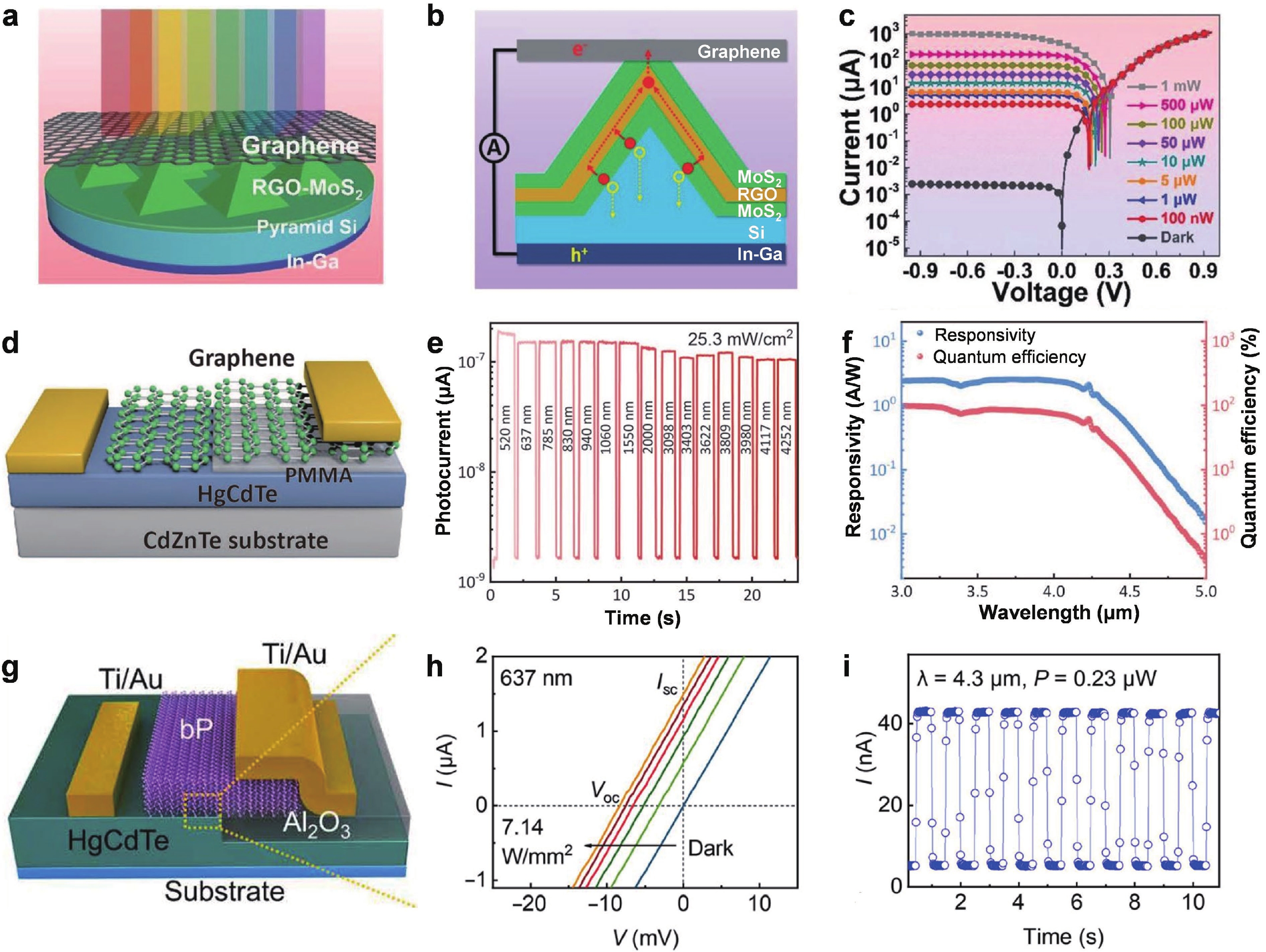
Xiao P, Mao J, Ding K, et al. Solution-processed 3D RGO-MoS 2/pyramid Si heterojunction for ultrahigh detectivity and ultra-broadband photodetection. Adv Mater, 2018, 30, 1801729 doi: 10.1002/adma.201801729 |
| [140] |
Chen W J, Liang R R, Zhang S Q, et al. Ultrahigh sensitive near-infrared photodetectors based on MoTe 2/germanium heterostructure. Nano Res, 2020, 13, 127 doi: 10.1007/s12274-019-2583-5 |
| [141] |
Lei W, Antoszewski J, Faraone L. Progress, challenges, and opportunities for HgCdTe infrared materials and detectors. Appl Phys Rev, 2015, 2, 041303 doi: 10.1063/1.4936577 |
| [142] |
Wang Y, Gu Y, Cui A L, et al. Fast uncooled mid-wavelength infrared photodetectors with heterostructures of van der Waals on epitaxial HgCdTe. Adv Mater, 2022, 34, 2107772 doi: 10.1002/adma.202107772 |
| [143] |
Jiao H X, Wang X D, Chen Y, et al. HgCdTe/black phosphorus van der Waals heterojunction for high-performance polarization-sensitive midwave infrared photodetector. Sci Adv, 2022, 8, eabn1811 doi: 10.1126/sciadv.abn1811 |
| [144] |
Nadupalli S, Kreisel J, Granzow T. Increasing bulk photovoltaic current by strain tuning. Sci Adv, 2019, 5, eaau9199 doi: 10.1126/sciadv.aau9199 |
| [145] |
Kushnir K, Wang M J, Fitzgerald P D, et al. Ultrafast zero-bias photocurrent in GeS nanosheets: promise for photovoltaics. ACS Energy Lett, 2017, 2, 1429 doi: 10.1021/acsenergylett.7b00330 |
| [146] |
Ai H Q, Liu D, Geng J Z, et al. Theoretical evidence of the spin-valley coupling and valley polarization in two-dimensional MoSi 2X 4 (X = N, P, and As). Phys Chem Chem Phys, 2021, 23, 3144 doi: 10.1039/D0CP05926A |
| [147] |
|
| [148] |
Park N G, Segawa H. Research direction toward theoretical efficiency in perovskite solar cells. ACS Photonics, 2018, 5, 2970 doi: 10.1021/acsphotonics.8b00124 |
| [149] |
Rühle S. Tabulated values of the Shockley–Queisser limit for single junction solar cells. Sol Energy, 2016, 130, 139 doi: 10.1016/j.solener.2016.02.015 |
| [150] |
Spanier J E, Fridkin V M, Rappe A M, et al. Power conversion efficiency exceeding the Shockley–Queisser limit in a ferroelectric insulator. Nat Photonics, 2016, 10, 611 doi: 10.1038/nphoton.2016.143 |
| [151] |
Han H, Song S, Lee J H, et al. Switchable photovoltaic effects in hexagonal manganite thin films having narrow band gaps. Chem Mater, 2015, 27, 7425 doi: 10.1021/acs.chemmater.5b03408 |
| [152] |
Bai Y, Jantunen H, Juuti J. Ferroelectric oxides for solar energy conversion, multi-source energy harvesting/sensing, and opto-ferroelectric applications. ChemSusChem, 2019, 12, 2540 doi: 10.1002/cssc.201900671 |
| [153] |
Zhang Y, Holder T, Ishizuka H, et al. Switchable magnetic bulk photovoltaic effect in the two-dimensional magnet CrI 3. Nat Commun, 2019, 10, 3783 doi: 10.1038/s41467-019-11832-3 |
| [154] |
Ding W J, Zhu J B, Wang Z, et al. Prediction of intrinsic two-dimensional ferroelectrics in In 2Se 3 and other III 2-VI 3 van der Waals materials. Nat Commun, 2017, 8, 14956 doi: 10.1038/ncomms14956 |
| [155] |
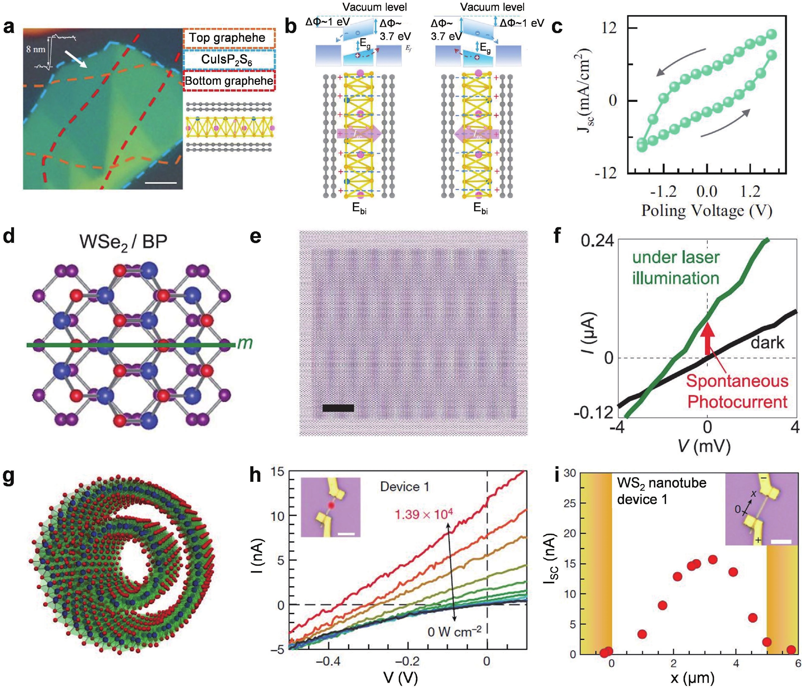
Li Y, Fu J, Mao X Y, et al. Enhanced bulk photovoltaic effect in two-dimensional ferroelectric CuInP 2S 6. Nat Commun, 2021, 12, 5896 doi: 10.1038/s41467-021-26200-3 |
| [156] |
Akamatsu T, Ideue T, Zhou L, et al. A van der Waals interface that creates in-plane polarization and a spontaneous photovoltaic effect. Science, 2021, 372, 68 doi: 10.1126/science.aaz9146 |
| [157] |
Qin F, Shi W, Ideue T, et al. Superconductivity in a chiral nanotube. Nat Commun, 2017, 8, 14465 doi: 10.1038/ncomms14465 |
| [158] |
Yadgarov L, Višić B, Abir T, et al. Strong light-matter interaction in tungsten disulfide nanotubes. Phys Chem Chem Phys, 2018, 20, 20812 doi: 10.1039/C8CP02245C |
| [159] |
Zhang C Y, Wang S, Yang L J, et al. High-performance photodetectors for visible and near-infrared lights based on individual WS 2 nanotubes. Appl Phys Lett, 2012, 100, 243101 doi: 10.1063/1.4729144 |
| [160] |
Jariwala D, Davoyan A R, Wong J, et al. Van der Waals materials for atomically-thin photovoltaics: promise and outlook. ACS Photonics, 2017, 4, 2962 doi: 10.1021/acsphotonics.7b01103 |
| [161] |
Schmidt H, Giustiniano F, Eda G. Electronic transport properties of transition metal dichalcogenide field-effect devices: surface and interface effects. Chem Soc Rev, 2015, 44, 7715 doi: 10.1039/C5CS00275C |
| [162] |
Vu Q A, Yu W J. Electronics and optoelectronics based on two-dimensional materials. J Korean Phys Soc, 2018, 73, 1 doi: 10.3938/jkps.73.1 |
| [163] |
Manzeli S, Ovchinnikov D, Pasquier D, et al. 2D transition metal dichalcogenides. Nat Rev Mater, 2017, 2, 17033 doi: 10.1038/natrevmats.2017.33 |
| [164] |
Lee D H, Lee J J, Kim Y S, et al. Remote modulation doping in van der Waals heterostructure transistors. Nat Electron, 2021, 4, 664 doi: 10.1038/s41928-021-00641-6 |
| [165] |
Li W S, Gong X S, Yu Z H, et al. Approaching the quantum limit in two-dimensional semiconductor contacts. Nature, 2023, 613, 274 doi: 10.1038/s41586-022-05431-4 |
| [166] |
|
| [167] |
Ma K Y, Zhang L N, Jin S, et al. Epitaxial single-crystal hexagonal boron nitride multilayers on Ni (111). Nature, 2022, 606, 88 doi: 10.1038/s41586-022-04745-7 |
| [168] |
Xu X L, Pan Y, Liu S, et al. Seeded 2D epitaxy of large-area single-crystal films of the van der Waals semiconductor 2H MoTe 2. Science, 2021, 372, 195 doi: 10.1126/science.abf5825 |
| [169] |
Yuan G W, Liu W L, Huang X L, et al. Stacking transfer of wafer-scale graphene-based van der Waals superlattices. Nat Commun, 2023, 14, 5457 doi: 10.1038/s41467-023-41296-5 |
| [170] |
Liu G Y, Tian Z A, Yang Z Y, et al. Graphene-assisted metal transfer printing for wafer-scale integration of metal electrodes and two-dimensional materials. Nat Electron, 2022, 5, 275 doi: 10.1038/s41928-022-00764-4 |


 DownLoad: