


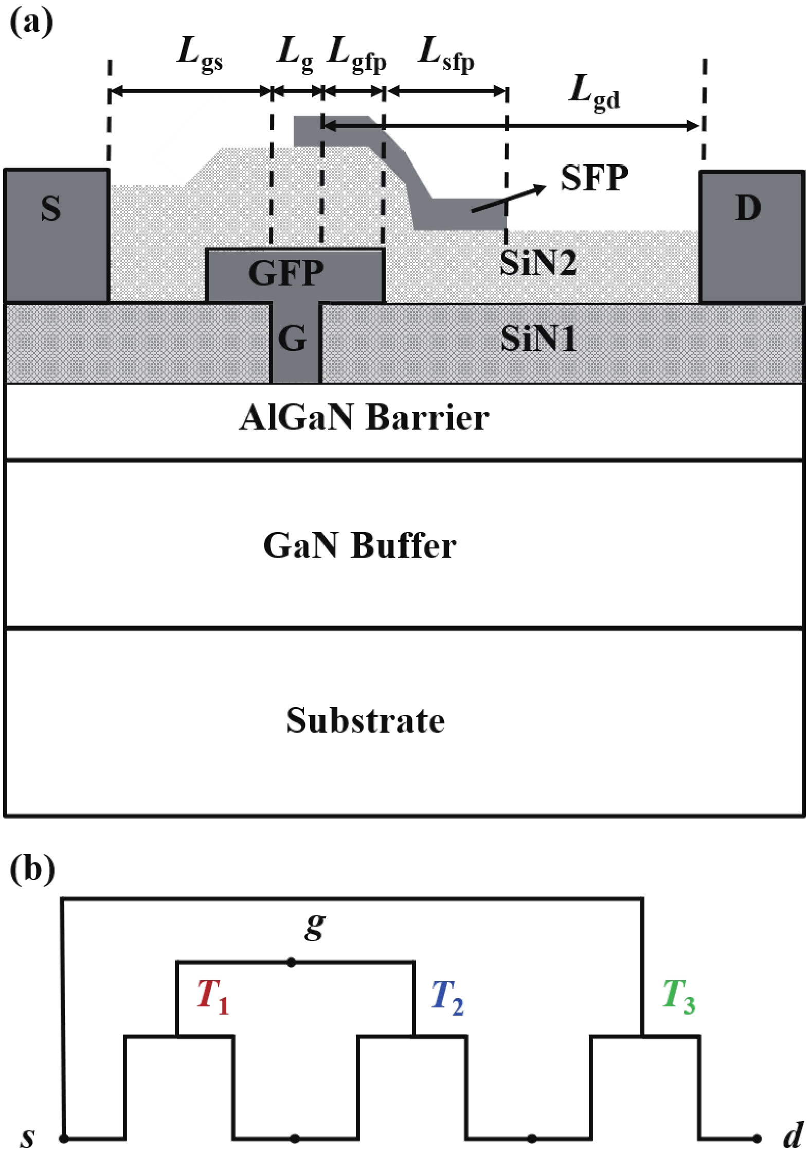
Fig. 1.
(Color online) (a) Cross section of the dual-field-plated GaN HEMT. (b) The equivalent circuit for the model with intrinsic transistor, gate-FP and source-FP.
ARTICLES
Jinye Wang, Jun Liu and Zhenxin Zhao
Corresponding author: Jun Liu, ljun77@hdu.edu.cn
Abstract: An accurate and novel small-signal equivalent circuit model for GaN high-electron-mobility transistors (HEMTs) is proposed, which considers a dual-field-plate (FP) made up of a gate-FP and a source-FP. The equivalent circuit of the overall model is composed of parasitic elements, intrinsic transistors, gate-FP, and source-FP networks. The equivalent circuit of the gate-FP is identical to that of the intrinsic transistor. In order to simplify the complexity of the model, a series combination of a resistor and a capacitor is employed to represent the source-FP. The analytical extraction procedure of the model parameters is presented based on the proposed equivalent circuit. The verification is carried out on a 4 × 250 μm GaN HEMT device with a gate-FP and a source-FP in a 0.45 μm technology. Compared with the classic model, the proposed novel small-signal model shows closer agreement with measured S-parameters in the range of 1.0 to 18.0 GHz.
Key words: small-signal model, dual field-plate(FP), GaN high-electron-mobility transistors (HEMT), parameter extraction
| [1] |
He J Q, Cheng W C, Wang Q, et al. Recent advances in GaN-based power HEMT devices. Adv Elect Mater, 2021, 7, 2001045 doi: 10.1002/aelm.202001045
|
| [2] |
Bahat-Treidel E, Hilt O, Brunner F, et al. AlGaN/GaN/AlGaN DH-HEMTs breakdown voltage enhancement using multiple grating field plates (MGFPs). IEEE Trans Electron Devices, 2010, 57, 1208 doi: 10.1109/TED.2010.2045705
|
| [3] |
Hu Q Y, Zeng F M, Cheng W C, et al. Reducing dynamic on-resistance of p-GaN gate HEMTs using dual field plate configurations. IEEE International Symposium on the Phys and Failure Analysis of Integrated Circuits (IPFA), 2020, 1 doi: 10.1109/IPFA49335.2020.9260581
|
| [4] |
Wu Y F, Saxler A, Moore M, et al. 30-W/mm GaN HEMTs by field plate optimization. IEEE Electron Device Lett, 2004, 25, 117 doi: 10.1109/LED.2003.822667
|
| [5] |
Xie G, Xu E, Lee J M, et al. Breakdown-voltage-enhancement technique for RF-based AlGaN/GaN HEMTs with a source-connected air-bridge field plate. IEEE Electron Device Lett, 2012, 33, 670 doi: 10.1109/LED.2012.2188492
|
| [6] |
Mao W, Fan J S, Du M, et al. Analysis of the modulation mechanisms of the electric field and breakdown performance in AlGaN/GaN HEMT with a T-shaped field-plate. Chinese Phys B, 2016, 25, 127305 doi: 10.1088/1674-1056/25/12/127305
|
| [7] |
Boles T, Carlson D, Xia L, et al. Effect of multi-field plates on the reverse breakdown and leakage characteristics of GaN-on-silicon HEMTs. Int Conference on Compound Semicond Manufacturing Technology, Denver, Colorado, 2014, 104
|
| [8] |
Amit M, Rawal D S, Sharma S, et al. Design and fabrication of multi-finger field plate for enhancement of AlGaN/GaN HEMT breakdown voltage. Def Sci J, 2018, 68, 290 doi: 10.14429/dsj.68.12134
|
| [9] |
Neha, Kumari V, Gupta M, et al. TCAD-based optimization of field plate length & passivation layer of AlGaN/GaN HEMT for higher cut-off frequency & breakdown voltage. IETE Tech Rev, 2022, 39, 63 doi: 10.1080/02564602.2020.1824624
|
| [10] |
Liu S J, Duan X L, Wang S L, et al. Optimization of dual field plate AlGaN/GaN HEMTs using artificial neural networks and particle swarm optimization algorithm. IEEE Trans Device Mater Reliab, 2023, 23, 204 doi: 10.1109/TDMR.2023.3246053
|
| [11] |
Marinković Z, Crupi G, Caddemi A, et al. A review on the artificial neural network applications for small-signal modeling of microwave FETs. Int J Numerical Modelling, 2020, 33, e2668 doi: 10.1002/jnm.2668
|
| [12] |
Khusro A, Husain S, Hashmi M S, et al. A reliable and fast ANN based behavioral modeling approach for GaN HEMT. Int Conference on Synthesis, Modeling, Analysis and Simulation Methods and Appl Circuit Design (SMACD), Lausanne, Switzerland, 2019, 277 doi: 10.1109/SMACD.2019.8795247
|
| [13] |
Khusro A, Husain S, Hashmi M S, et al. Small signal behavioral modeling technique of GaN high electron mobility transistor using artificial neural network: An accurate, fast, and reliable approach. Int J RF Microw Comput Aided Eng, 2020, 30, e22112 doi: 10.1002/mmce.22112
|
| [14] |
Khusro A, Husain S, Hashmi M S, et al. A generic and efficient globalized kernel mapping-based small-signal behavioral modeling for GaN HEMT. IEEE Access, 2020, 8, 195046 doi: 10.1109/ACCESS.2020.3033788
|
| [15] |
Guan R L, Zhu H S, Che W Q, et al. An improved parameter extraction approach for GaN HEMT small-signal modelling. 2020 IEEE MTT-S International Wireless Symposium (IWS), Harbin, China, 2022, 1 doi: 10.1109/IWS55252.2022.9977881
|
| [16] |
Fan Q, Leach J H, Morkoc H. Small signal equivalent circuit modeling for AlGaN/GaN HFET: Hybrid extraction method for determining circuit elements of AlGaN/GaN HFET. Proc IEEE, 2010, 98, 1140 doi: 10.1109/JPROC.2010.2044630
|
| [17] |
Majumder A, Chatterjee S, Chatterjee S, et al. Optimization of small-signal model of GaN HEMT by using evolutionary algorithms. IEEE Microw Wirel Compon Lett, 2017, 27, 362 doi: 10.1109/LMWC.2017.2678437
|
| [18] |
Du J F, Wang K, Yin C G, et al. Small signal modeling of 90 nm gate-length AlGaN/GaN HEMTs considering mesa edge effects. 2014 IEEE International Conference on Electron Devices and Solid-State Circuits, Chengdu, China, 2014, 1 doi: 10.1109/EDSSC.2014.7061240
|
| [19] |
Jia Y H, Xu Y H, Wu Y Q, et al. A robust small-signal equivalent circuit model for AlGaN/GaN HEMTs up to 110 GHz. 2016 IEEE MTT-S International Microwave Workshop Series on Advanced Materials and Processes for RF and THz Applications (IMWS-AMP), Chengdu, China, 2016, 1 doi: 10.1109/IMWS-AMP.2016.7588419
|
| [20] |
Pei Y, Al-Saman A A, Yin C G, et al. An intrinsic small-signal equivalent circuit model for AlGaN/GaN HEMT considering the momentum balance equation. IEEE J Electron Devices Soc, 2021, 9, 1060 doi: 10.1109/JEDS.2021.3124327
|
| [21] |
Karmalkar S, Mishra U K. Enhancement of breakdown voltage in AlGaN/GaN high electron mobility transistors using a field plate. IEEE Trans Electron Devices, 2001, 48, 1515 doi: 10.1109/16.936500
|
| [22] |
Wen Z, Xu Y H, Wang C S, et al. An efficient parameter extraction method for GaN HEMT small-signal equivalent circuit model. Int J Numerical Modelling, 2017, 30, e2127 doi: 10.1002/jnm.2127
|
| [23] |
White P M, Healy R M. Improved equivalent circuit for determination of MESFET and HEMT parasitic capacitances from "Coldfet" measurements. IEEE Microw Guid Wave Lett, 1993, 3, 453 doi: 10.1109/75.251398
|
| [24] |
Jarndal A, Kompa G. A new small-signal modeling approach applied to GaN devices. IEEE Trans Microw Theory Tech, 2005, 53, 3440 doi: 10.1109/TMTT.2005.857332
|
| [25] |
Liu J, Ren K, Sun L L, et al. A novel small-signal model for bulk FinFETs accommodating self-heating behaviors. IEEE Electron Device Lett, 2017, 38, 839 doi: 10.1109/LED.2017.2707283
|
| [26] |
Wang J Y, Liu J, Chen Z F, et al. An accurate parameter extraction method for small signal model of CNFET. Int J Numerical Modelling, 2021, 34, e2896 doi: 10.1002/jnm.2896
|
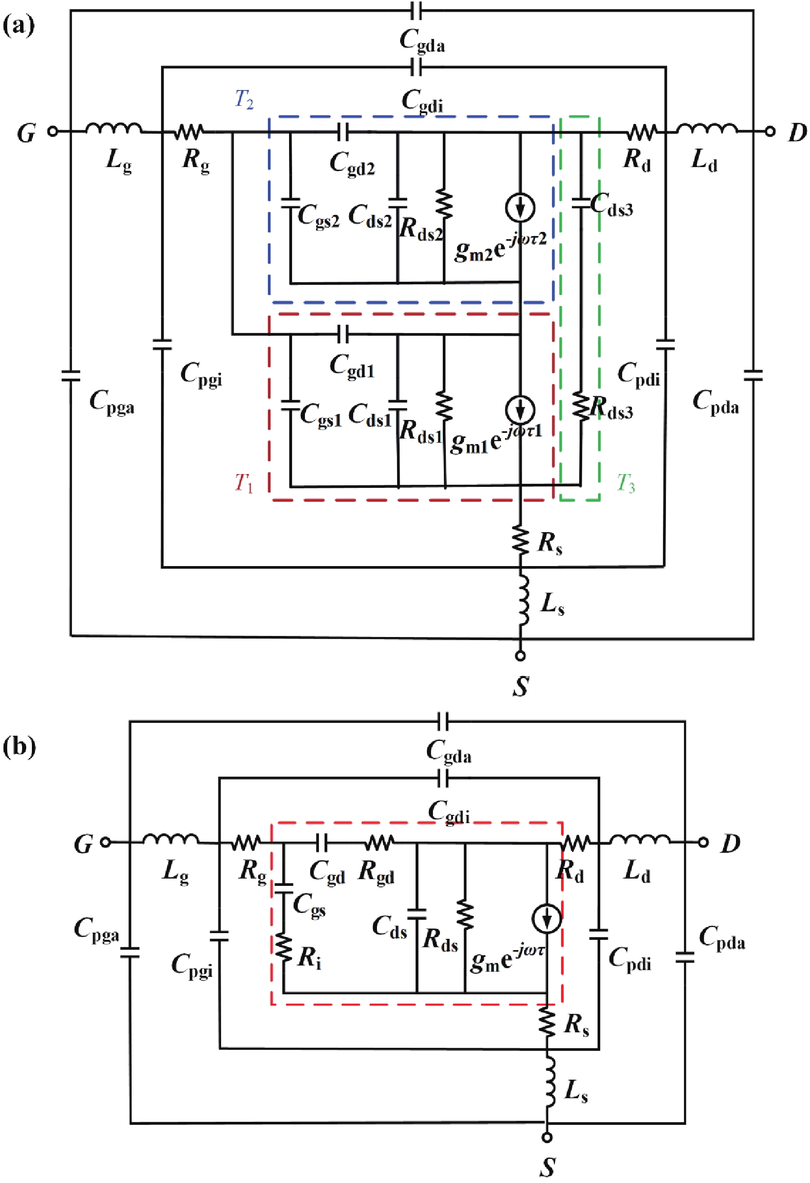
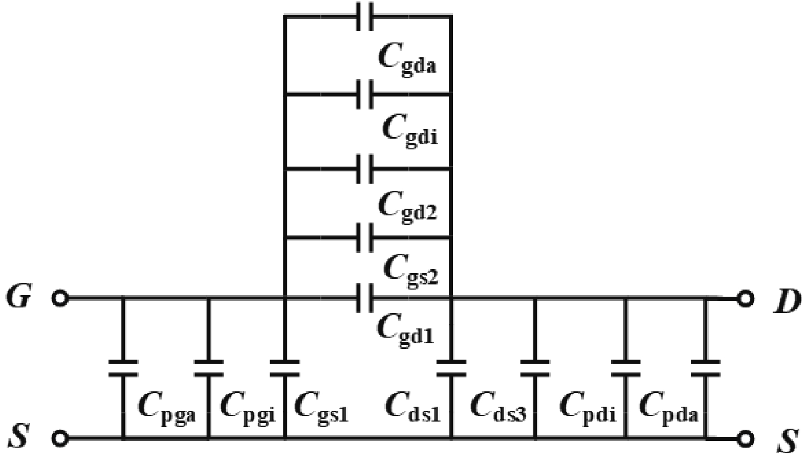
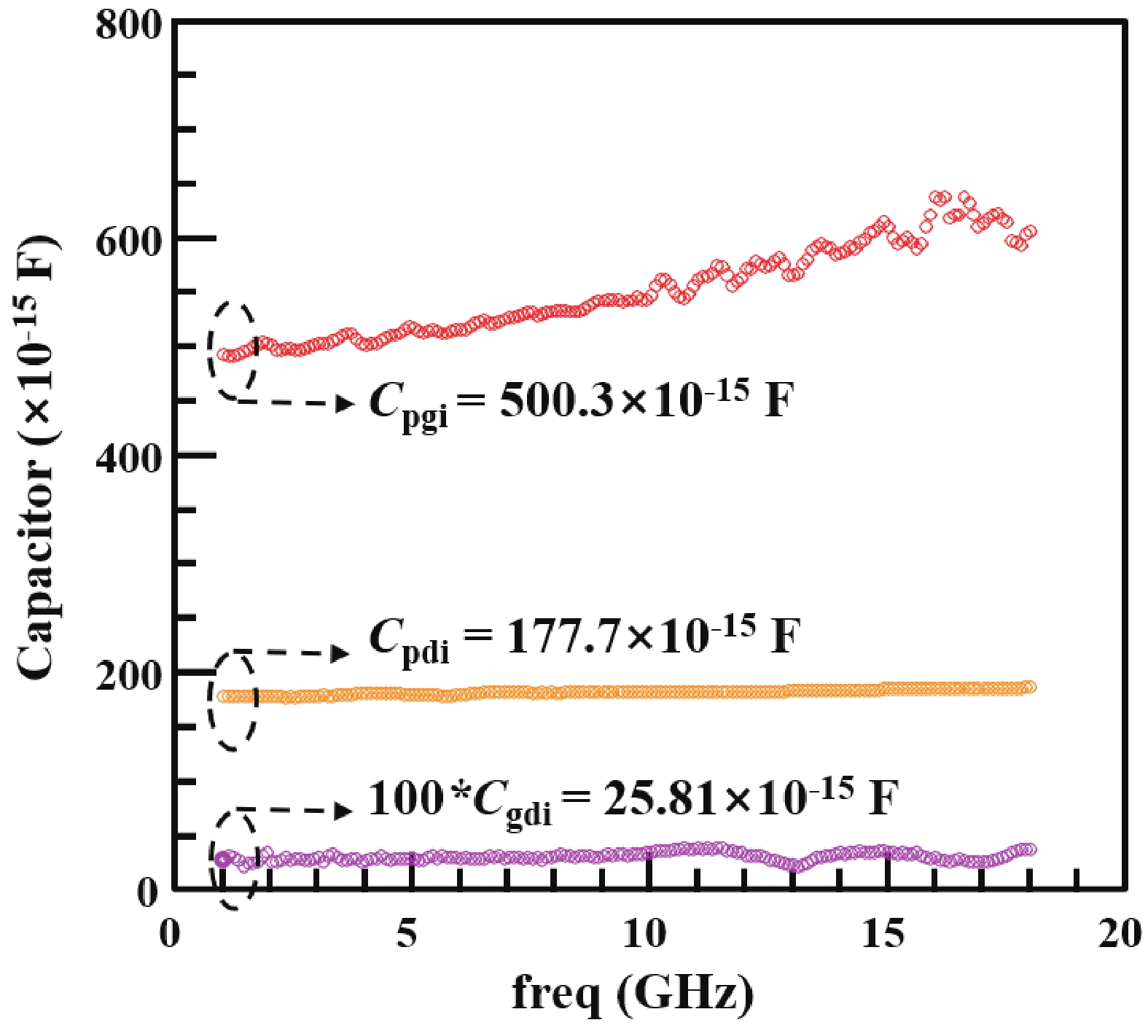
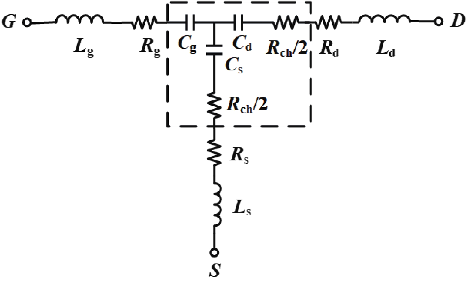
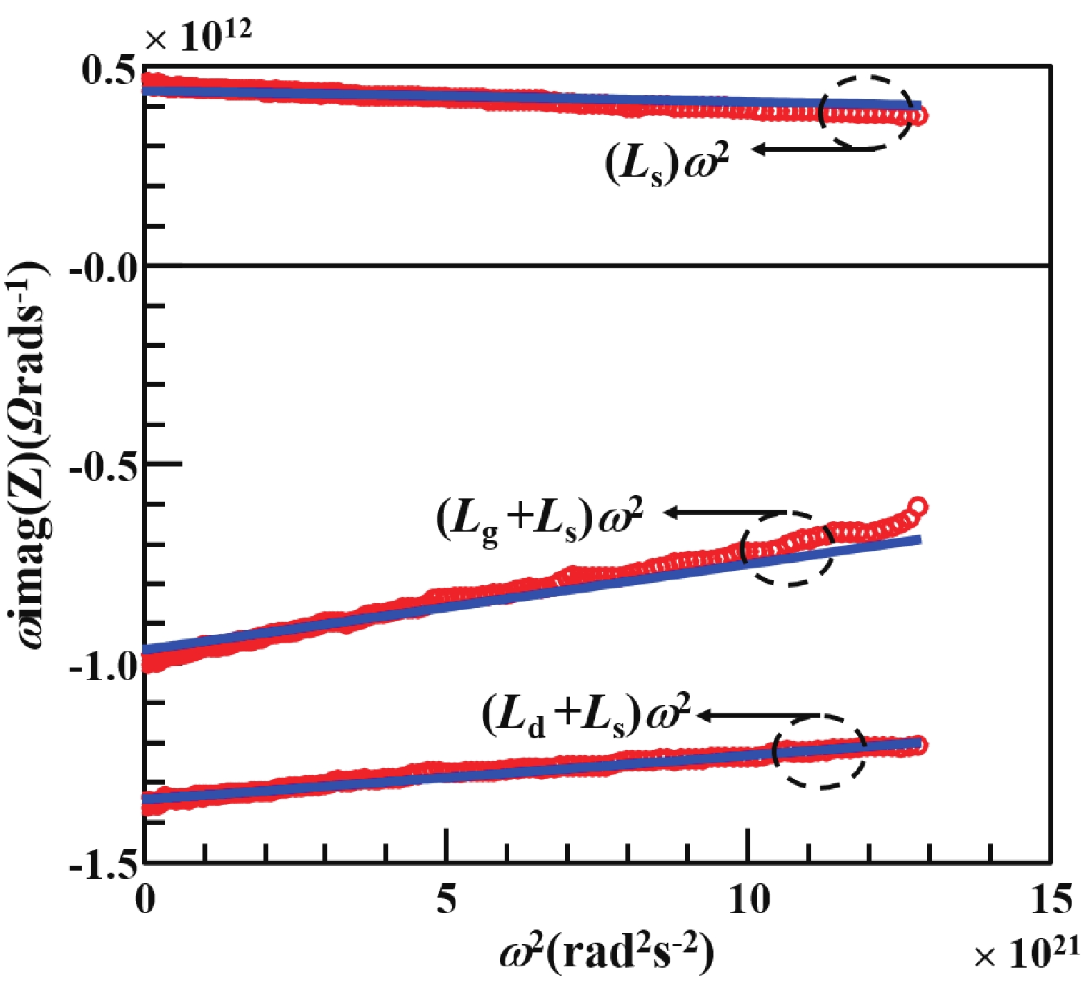
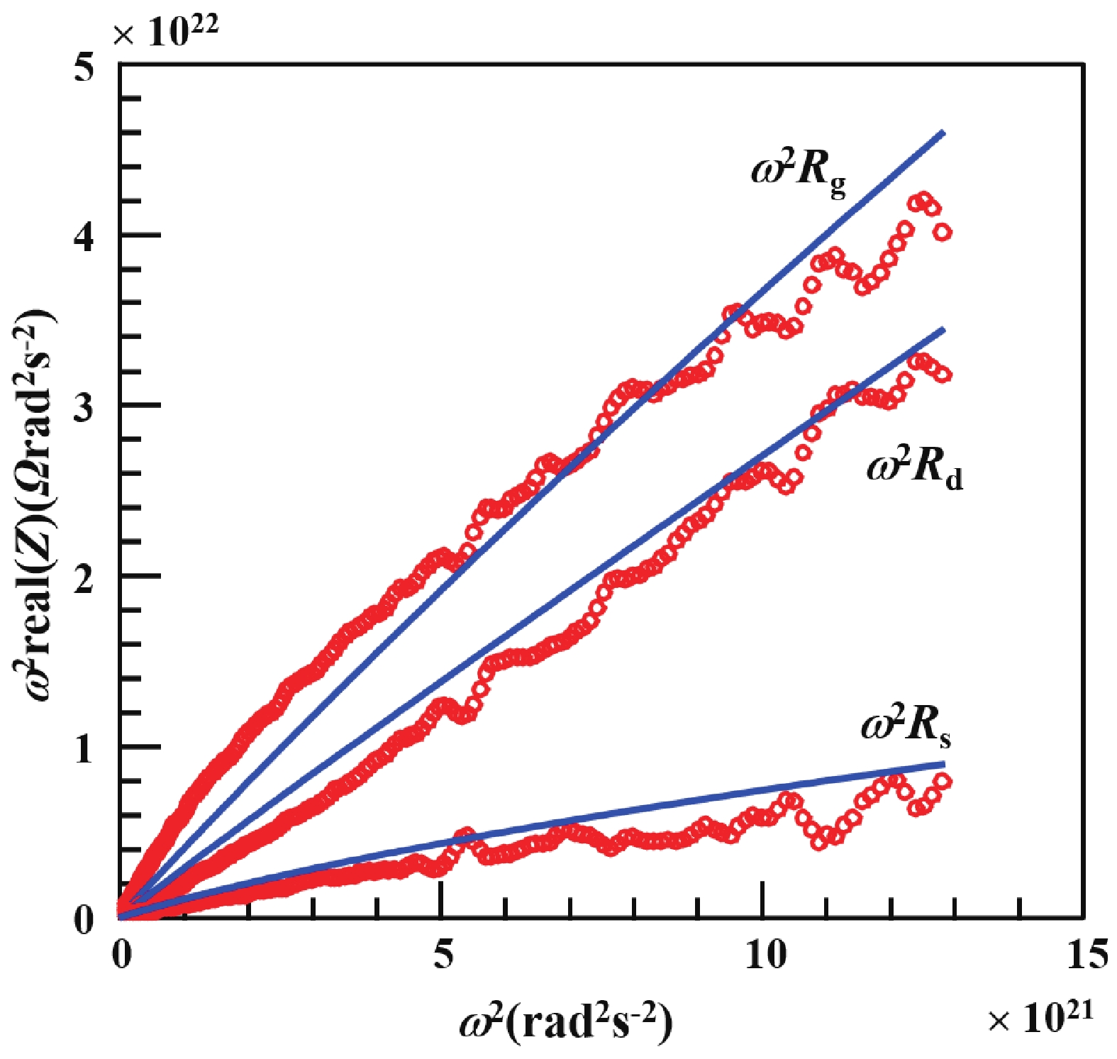
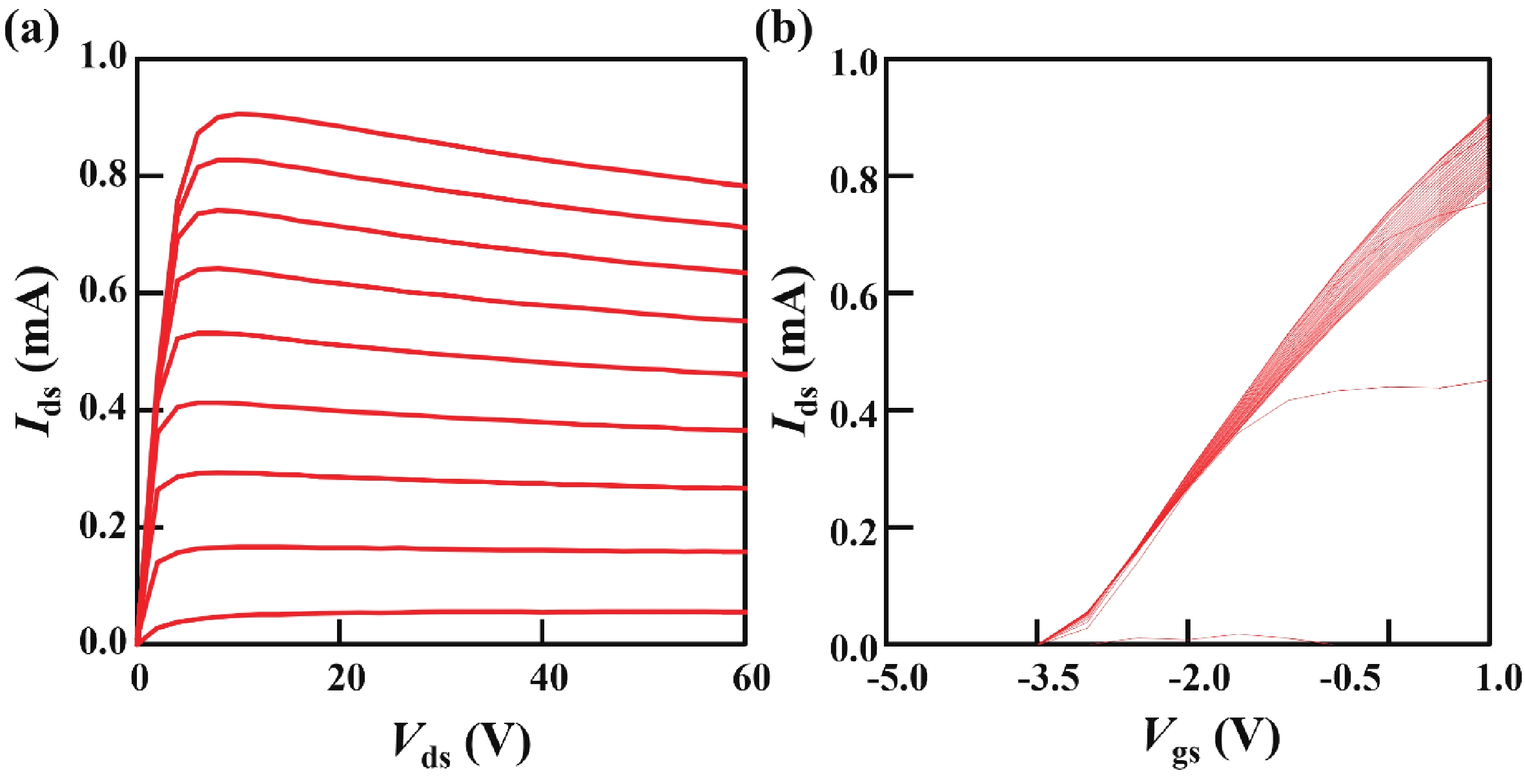
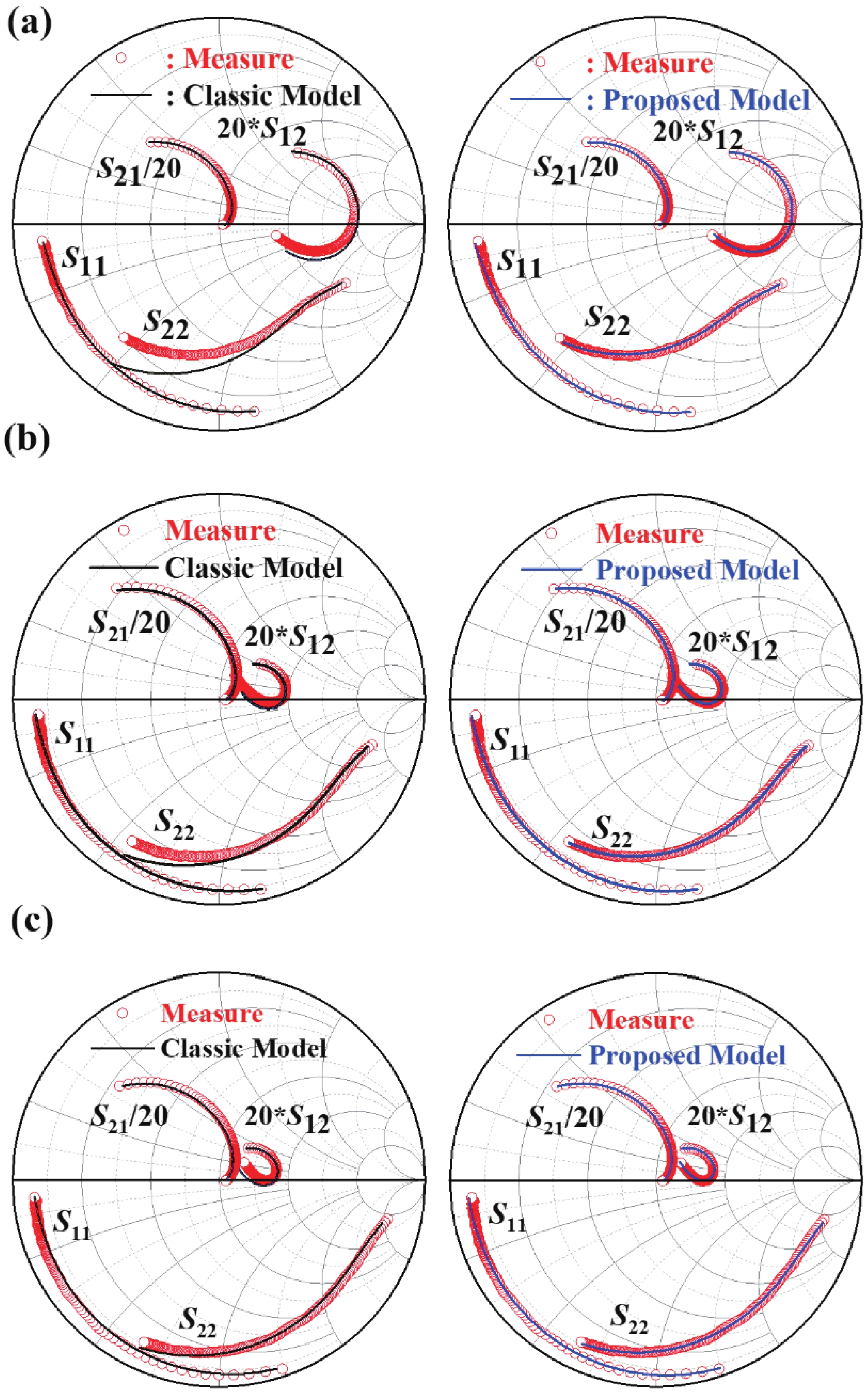
Table 1. The proposed and classical small-signal model parameters’ initially extracted and optimized values for a 4 × 250 μm dual-field-plate GaN HEMT.
| Parameter | Extracted value | Optimized parameter | |
| Extrinsic parameters | |||
| Cpga, Cgda, Cpda (fF) | 50.67, 0.1297, 59.22 | 50.67, 0.1297, 59.22 | |
| Proposed model (Classic model) |
Cpgi, Cgdi, Cpdi (fF) | 500.3, 0.2581, 177.7 | 508.5(375.7), 0.258(0.258), 177.7(158.3) |
| Lg, Ld, Ls (pH) | 15.42, 5.318, 2.660 | 15.42(15.42), 6.783(6.783), 4.288(2.892) | |
| Rg, Rd, Rs (Ω) | 3.254, 2.458, 0.6439 | 3.382(3.382), 2.628(2.458), 0.546(0.635) | |
| Bias-independent parameters at Vds = 28 V, Vgs = 1 V | |||
| Proposed model |
Cgs1, Cgd1, Cds1 (fF) | 1730, 474.4, 38.87 | 950.9, 229.0, 46.39 |
| Cgs2, Cgd2, Cds2, Cds3 (fF) | 474.4, 63.87, 38.87,77.73 | 338.7, 35.40, 20.31, 134.5 | |
| Rds1, Rds2, Rds3 (Ω) | 51.89, 375.0, 51.89 | 16.01, 133.8, 50.01 | |
| gm1, gm2 (mS) | 144.3, 144.3 | 202.2, 110.8 | |
| τ1, τ2 (pS) | 8.599, 8.599 | 4.309, 3.677 | |
| Classic model | Cgs, Cgd, Cds (fF) | 1952, 57.76, 130.6 | 1952, 57.76, 137.5 |
| Ri, Rgd, Rds (Ω) | 1.654, 12.4, 319.0 | 1.654, 12.36, 339.1 | |
| gm (mS), τ (pS) | 144.9, 6.612 | 180.4, 8.664 | |
| Bias-independent parameters at Vds = 40 V, Vgs = −1 V | |||
| Proposed model | Cgs1, Cgd1, Cds1 (fF) | 1665, 480.3, 28.19 | 913.1, 244.3, 9.731 |
| Cgs2, Cgd2, Cds2, Cds3 (fF) | 480.3, 27.25, 28.19, 56.37 | 539.1, 13.13, 23.39, 60.77 | |
| Rds1, Rds2, Rds3 (Ω) | 43.7, 651.3, 325.6 | 6.449, 351.8, 44.1 | |
| gm1, gm2 (mS) | 179.3, 179.3 | 207.6, 179.3 | |
| τ1, τ2 (pS) | 7.714, 7.714 | 4.609, 3.881 | |
| Classic model | Cgs, Cgd, Cds (fF) | 2113, 32.98, 85.88 | 2169, 24.37, 114.4 |
| Ri, Rgd, Rds (Ω) | 0.8043, 189.8, 491.4 | 0.2213, 50.89, 446.1 | |
| gm (mS), τ (pS) | 208.9, 5.676 | 243.7, 5.087 | |
| Bias-independent parameters at Vds = 48 V, Vgs = −3 V | |||
| Proposed model |
Cgs1, Cgd1, Cds1 (fF) | 1837, 528.5, 16.96 | 976.7, 294.8, 15.50 |
| Cgs2, Cgd2, Cds2, Cds3 (fF) | 528.5, 32.31, 16.96, 33.92 | 660.2, 10.91, 13.66, 104.7 | |
| Rds1, Rds2, Rds3 (Ω) | 167.8, 721.5, 360.7 | 8.317, 208.9, 28.45 | |
| gm1, gm2 (mS) | 191.3, 191.3 | 288.0, 167.1 | |
| τ1, τ2 (pS) | 9.060, 9.060 | 4.307, 3.624 | |
| Classic model | Cgs, Cgd, Cds (fF) | 1872, 26.95, 75.44 | 2003, 19.96, 100.9 |
| Ri, Rgd, Rds (Ω) | 0.2668, 196.4, 815.3 | 0.1052, 45.61, 621.7 | |
| gm (mS), τ (pS) | 186.3, 5.507 | 202.6, 3.837 | |
 DownLoad: CSV
Table 2. Comparison of error of the proposed and the classical model under three different bias conditions.
| Bias condition | Model | E11 (%) | E12 (%) | E21 (%) | E22 (%) |
| Vds = 28 V, Vgs = 1 V | Classic model | 0.579 | 14.63 | 17.73 | 10.56 |
| Proposed model | 1.549 | 3.192 | 6.872 | 2.393 | |
| Vds = 40 V, Vgs = −1 V | Classic model | 1.036 | 30.19 | 8.84 | 5.511 |
| Proposed model | 1.176 | 4.797 | 4.072 | 2.173 | |
| Vds = 48 V, Vgs = −3 V | Classic model | 2.019 | 19.11 | 11.52 | 4.269 |
| Proposed model | 1.314 | 9.284 | 4.511 | 2.576 |
DownLoad: CSV
| [1] |
He J Q, Cheng W C, Wang Q, et al. Recent advances in GaN-based power HEMT devices. Adv Elect Mater, 2021, 7, 2001045 doi: 10.1002/aelm.202001045
|
| [2] |
Bahat-Treidel E, Hilt O, Brunner F, et al. AlGaN/GaN/AlGaN DH-HEMTs breakdown voltage enhancement using multiple grating field plates (MGFPs). IEEE Trans Electron Devices, 2010, 57, 1208 doi: 10.1109/TED.2010.2045705
|
| [3] |
Hu Q Y, Zeng F M, Cheng W C, et al. Reducing dynamic on-resistance of p-GaN gate HEMTs using dual field plate configurations. IEEE International Symposium on the Phys and Failure Analysis of Integrated Circuits (IPFA), 2020, 1 doi: 10.1109/IPFA49335.2020.9260581
|
| [4] |
Wu Y F, Saxler A, Moore M, et al. 30-W/mm GaN HEMTs by field plate optimization. IEEE Electron Device Lett, 2004, 25, 117 doi: 10.1109/LED.2003.822667
|
| [5] |
Xie G, Xu E, Lee J M, et al. Breakdown-voltage-enhancement technique for RF-based AlGaN/GaN HEMTs with a source-connected air-bridge field plate. IEEE Electron Device Lett, 2012, 33, 670 doi: 10.1109/LED.2012.2188492
|
| [6] |
Mao W, Fan J S, Du M, et al. Analysis of the modulation mechanisms of the electric field and breakdown performance in AlGaN/GaN HEMT with a T-shaped field-plate. Chinese Phys B, 2016, 25, 127305 doi: 10.1088/1674-1056/25/12/127305
|
| [7] |
Boles T, Carlson D, Xia L, et al. Effect of multi-field plates on the reverse breakdown and leakage characteristics of GaN-on-silicon HEMTs. Int Conference on Compound Semicond Manufacturing Technology, Denver, Colorado, 2014, 104
|
| [8] |
Amit M, Rawal D S, Sharma S, et al. Design and fabrication of multi-finger field plate for enhancement of AlGaN/GaN HEMT breakdown voltage. Def Sci J, 2018, 68, 290 doi: 10.14429/dsj.68.12134
|
| [9] |
Neha, Kumari V, Gupta M, et al. TCAD-based optimization of field plate length & passivation layer of AlGaN/GaN HEMT for higher cut-off frequency & breakdown voltage. IETE Tech Rev, 2022, 39, 63 doi: 10.1080/02564602.2020.1824624
|
| [10] |
Liu S J, Duan X L, Wang S L, et al. Optimization of dual field plate AlGaN/GaN HEMTs using artificial neural networks and particle swarm optimization algorithm. IEEE Trans Device Mater Reliab, 2023, 23, 204 doi: 10.1109/TDMR.2023.3246053
|
| [11] |
Marinković Z, Crupi G, Caddemi A, et al. A review on the artificial neural network applications for small-signal modeling of microwave FETs. Int J Numerical Modelling, 2020, 33, e2668 doi: 10.1002/jnm.2668
|
| [12] |
Khusro A, Husain S, Hashmi M S, et al. A reliable and fast ANN based behavioral modeling approach for GaN HEMT. Int Conference on Synthesis, Modeling, Analysis and Simulation Methods and Appl Circuit Design (SMACD), Lausanne, Switzerland, 2019, 277 doi: 10.1109/SMACD.2019.8795247
|
| [13] |
Khusro A, Husain S, Hashmi M S, et al. Small signal behavioral modeling technique of GaN high electron mobility transistor using artificial neural network: An accurate, fast, and reliable approach. Int J RF Microw Comput Aided Eng, 2020, 30, e22112 doi: 10.1002/mmce.22112
|
| [14] |
Khusro A, Husain S, Hashmi M S, et al. A generic and efficient globalized kernel mapping-based small-signal behavioral modeling for GaN HEMT. IEEE Access, 2020, 8, 195046 doi: 10.1109/ACCESS.2020.3033788
|
| [15] |
Guan R L, Zhu H S, Che W Q, et al. An improved parameter extraction approach for GaN HEMT small-signal modelling. 2020 IEEE MTT-S International Wireless Symposium (IWS), Harbin, China, 2022, 1 doi: 10.1109/IWS55252.2022.9977881
|
| [16] |
Fan Q, Leach J H, Morkoc H. Small signal equivalent circuit modeling for AlGaN/GaN HFET: Hybrid extraction method for determining circuit elements of AlGaN/GaN HFET. Proc IEEE, 2010, 98, 1140 doi: 10.1109/JPROC.2010.2044630
|
| [17] |
Majumder A, Chatterjee S, Chatterjee S, et al. Optimization of small-signal model of GaN HEMT by using evolutionary algorithms. IEEE Microw Wirel Compon Lett, 2017, 27, 362 doi: 10.1109/LMWC.2017.2678437
|
| [18] |
Du J F, Wang K, Yin C G, et al. Small signal modeling of 90 nm gate-length AlGaN/GaN HEMTs considering mesa edge effects. 2014 IEEE International Conference on Electron Devices and Solid-State Circuits, Chengdu, China, 2014, 1 doi: 10.1109/EDSSC.2014.7061240
|
| [19] |
Jia Y H, Xu Y H, Wu Y Q, et al. A robust small-signal equivalent circuit model for AlGaN/GaN HEMTs up to 110 GHz. 2016 IEEE MTT-S International Microwave Workshop Series on Advanced Materials and Processes for RF and THz Applications (IMWS-AMP), Chengdu, China, 2016, 1 doi: 10.1109/IMWS-AMP.2016.7588419
|
| [20] |
Pei Y, Al-Saman A A, Yin C G, et al. An intrinsic small-signal equivalent circuit model for AlGaN/GaN HEMT considering the momentum balance equation. IEEE J Electron Devices Soc, 2021, 9, 1060 doi: 10.1109/JEDS.2021.3124327
|
| [21] |
Karmalkar S, Mishra U K. Enhancement of breakdown voltage in AlGaN/GaN high electron mobility transistors using a field plate. IEEE Trans Electron Devices, 2001, 48, 1515 doi: 10.1109/16.936500
|
| [22] |
Wen Z, Xu Y H, Wang C S, et al. An efficient parameter extraction method for GaN HEMT small-signal equivalent circuit model. Int J Numerical Modelling, 2017, 30, e2127 doi: 10.1002/jnm.2127
|
| [23] |
White P M, Healy R M. Improved equivalent circuit for determination of MESFET and HEMT parasitic capacitances from "Coldfet" measurements. IEEE Microw Guid Wave Lett, 1993, 3, 453 doi: 10.1109/75.251398
|
| [24] |
Jarndal A, Kompa G. A new small-signal modeling approach applied to GaN devices. IEEE Trans Microw Theory Tech, 2005, 53, 3440 doi: 10.1109/TMTT.2005.857332
|
| [25] |
Liu J, Ren K, Sun L L, et al. A novel small-signal model for bulk FinFETs accommodating self-heating behaviors. IEEE Electron Device Lett, 2017, 38, 839 doi: 10.1109/LED.2017.2707283
|
| [26] |
Wang J Y, Liu J, Chen Z F, et al. An accurate parameter extraction method for small signal model of CNFET. Int J Numerical Modelling, 2021, 34, e2896 doi: 10.1002/jnm.2896
|


Article views: 236 Times PDF downloads: 38 Times Cited by: 0 Times
Received: 20 December 2023 Revised: 18 January 2024 Online: Accepted Manuscript: 23 February 2024Uncorrected proof: 26 February 2024Published: 10 May 2024
| Citation: |
Jinye Wang, Jun Liu, Zhenxin Zhao. A novel small-signal equivalent circuit model for GaN HEMTs incorporating a dual-field-plate[J]. Journal of Semiconductors, 2024, 45(5): 052302. doi: 10.1088/1674-4926/45/5/052302
J Y Wang, J Liu, and Z X Zhao, A novel small-signal equivalent circuit model for GaN HEMTs incorporating a dual-field-plate[J]. J. Semicond., 2024, 45(5), 052302 doi: 10.1088/1674-4926/45/5/052302
Export: BibTex EndNote

|
| [1] |
He J Q, Cheng W C, Wang Q, et al. Recent advances in GaN-based power HEMT devices. Adv Elect Mater, 2021, 7, 2001045 doi: 10.1002/aelm.202001045
|
| [2] |
Bahat-Treidel E, Hilt O, Brunner F, et al. AlGaN/GaN/AlGaN DH-HEMTs breakdown voltage enhancement using multiple grating field plates (MGFPs). IEEE Trans Electron Devices, 2010, 57, 1208 doi: 10.1109/TED.2010.2045705
|
| [3] |
Hu Q Y, Zeng F M, Cheng W C, et al. Reducing dynamic on-resistance of p-GaN gate HEMTs using dual field plate configurations. IEEE International Symposium on the Phys and Failure Analysis of Integrated Circuits (IPFA), 2020, 1 doi: 10.1109/IPFA49335.2020.9260581
|
| [4] |
Wu Y F, Saxler A, Moore M, et al. 30-W/mm GaN HEMTs by field plate optimization. IEEE Electron Device Lett, 2004, 25, 117 doi: 10.1109/LED.2003.822667
|
| [5] |
Xie G, Xu E, Lee J M, et al. Breakdown-voltage-enhancement technique for RF-based AlGaN/GaN HEMTs with a source-connected air-bridge field plate. IEEE Electron Device Lett, 2012, 33, 670 doi: 10.1109/LED.2012.2188492
|
| [6] |
Mao W, Fan J S, Du M, et al. Analysis of the modulation mechanisms of the electric field and breakdown performance in AlGaN/GaN HEMT with a T-shaped field-plate. Chinese Phys B, 2016, 25, 127305 doi: 10.1088/1674-1056/25/12/127305
|
| [7] |
Boles T, Carlson D, Xia L, et al. Effect of multi-field plates on the reverse breakdown and leakage characteristics of GaN-on-silicon HEMTs. Int Conference on Compound Semicond Manufacturing Technology, Denver, Colorado, 2014, 104
|
| [8] |
Amit M, Rawal D S, Sharma S, et al. Design and fabrication of multi-finger field plate for enhancement of AlGaN/GaN HEMT breakdown voltage. Def Sci J, 2018, 68, 290 doi: 10.14429/dsj.68.12134
|
| [9] |
Neha, Kumari V, Gupta M, et al. TCAD-based optimization of field plate length & passivation layer of AlGaN/GaN HEMT for higher cut-off frequency & breakdown voltage. IETE Tech Rev, 2022, 39, 63 doi: 10.1080/02564602.2020.1824624
|
| [10] |
Liu S J, Duan X L, Wang S L, et al. Optimization of dual field plate AlGaN/GaN HEMTs using artificial neural networks and particle swarm optimization algorithm. IEEE Trans Device Mater Reliab, 2023, 23, 204 doi: 10.1109/TDMR.2023.3246053
|
| [11] |
Marinković Z, Crupi G, Caddemi A, et al. A review on the artificial neural network applications for small-signal modeling of microwave FETs. Int J Numerical Modelling, 2020, 33, e2668 doi: 10.1002/jnm.2668
|
| [12] |
Khusro A, Husain S, Hashmi M S, et al. A reliable and fast ANN based behavioral modeling approach for GaN HEMT. Int Conference on Synthesis, Modeling, Analysis and Simulation Methods and Appl Circuit Design (SMACD), Lausanne, Switzerland, 2019, 277 doi: 10.1109/SMACD.2019.8795247
|
| [13] |
Khusro A, Husain S, Hashmi M S, et al. Small signal behavioral modeling technique of GaN high electron mobility transistor using artificial neural network: An accurate, fast, and reliable approach. Int J RF Microw Comput Aided Eng, 2020, 30, e22112 doi: 10.1002/mmce.22112
|
| [14] |
Khusro A, Husain S, Hashmi M S, et al. A generic and efficient globalized kernel mapping-based small-signal behavioral modeling for GaN HEMT. IEEE Access, 2020, 8, 195046 doi: 10.1109/ACCESS.2020.3033788
|
| [15] |
Guan R L, Zhu H S, Che W Q, et al. An improved parameter extraction approach for GaN HEMT small-signal modelling. 2020 IEEE MTT-S International Wireless Symposium (IWS), Harbin, China, 2022, 1 doi: 10.1109/IWS55252.2022.9977881
|
| [16] |
Fan Q, Leach J H, Morkoc H. Small signal equivalent circuit modeling for AlGaN/GaN HFET: Hybrid extraction method for determining circuit elements of AlGaN/GaN HFET. Proc IEEE, 2010, 98, 1140 doi: 10.1109/JPROC.2010.2044630
|
| [17] |
Majumder A, Chatterjee S, Chatterjee S, et al. Optimization of small-signal model of GaN HEMT by using evolutionary algorithms. IEEE Microw Wirel Compon Lett, 2017, 27, 362 doi: 10.1109/LMWC.2017.2678437
|
| [18] |
Du J F, Wang K, Yin C G, et al. Small signal modeling of 90 nm gate-length AlGaN/GaN HEMTs considering mesa edge effects. 2014 IEEE International Conference on Electron Devices and Solid-State Circuits, Chengdu, China, 2014, 1 doi: 10.1109/EDSSC.2014.7061240
|
| [19] |
Jia Y H, Xu Y H, Wu Y Q, et al. A robust small-signal equivalent circuit model for AlGaN/GaN HEMTs up to 110 GHz. 2016 IEEE MTT-S International Microwave Workshop Series on Advanced Materials and Processes for RF and THz Applications (IMWS-AMP), Chengdu, China, 2016, 1 doi: 10.1109/IMWS-AMP.2016.7588419
|
| [20] |
Pei Y, Al-Saman A A, Yin C G, et al. An intrinsic small-signal equivalent circuit model for AlGaN/GaN HEMT considering the momentum balance equation. IEEE J Electron Devices Soc, 2021, 9, 1060 doi: 10.1109/JEDS.2021.3124327
|
| [21] |
Karmalkar S, Mishra U K. Enhancement of breakdown voltage in AlGaN/GaN high electron mobility transistors using a field plate. IEEE Trans Electron Devices, 2001, 48, 1515 doi: 10.1109/16.936500
|
| [22] |
Wen Z, Xu Y H, Wang C S, et al. An efficient parameter extraction method for GaN HEMT small-signal equivalent circuit model. Int J Numerical Modelling, 2017, 30, e2127 doi: 10.1002/jnm.2127
|
| [23] |
White P M, Healy R M. Improved equivalent circuit for determination of MESFET and HEMT parasitic capacitances from "Coldfet" measurements. IEEE Microw Guid Wave Lett, 1993, 3, 453 doi: 10.1109/75.251398
|
| [24] |
Jarndal A, Kompa G. A new small-signal modeling approach applied to GaN devices. IEEE Trans Microw Theory Tech, 2005, 53, 3440 doi: 10.1109/TMTT.2005.857332
|
| [25] |
Liu J, Ren K, Sun L L, et al. A novel small-signal model for bulk FinFETs accommodating self-heating behaviors. IEEE Electron Device Lett, 2017, 38, 839 doi: 10.1109/LED.2017.2707283
|
| [26] |
Wang J Y, Liu J, Chen Z F, et al. An accurate parameter extraction method for small signal model of CNFET. Int J Numerical Modelling, 2021, 34, e2896 doi: 10.1002/jnm.2896
|

 WeChat ID
Journal of Semiconductors © 2017 All Rights Reserved 京ICP备05085259号-2


