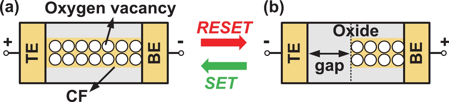
Fig. 1.
(Color online) Illustration of RRAM device at (a) switched on state and (b) switched off state.
ARTICLES
Yuhang Zhang1, 2, Guanghui He1, 2, Feng Zhang3, Yongfu Li1, 2, and Guoxing Wang1, 2
Corresponding author: Yongfu Li, yongfu.li@sjtu.edu.cn
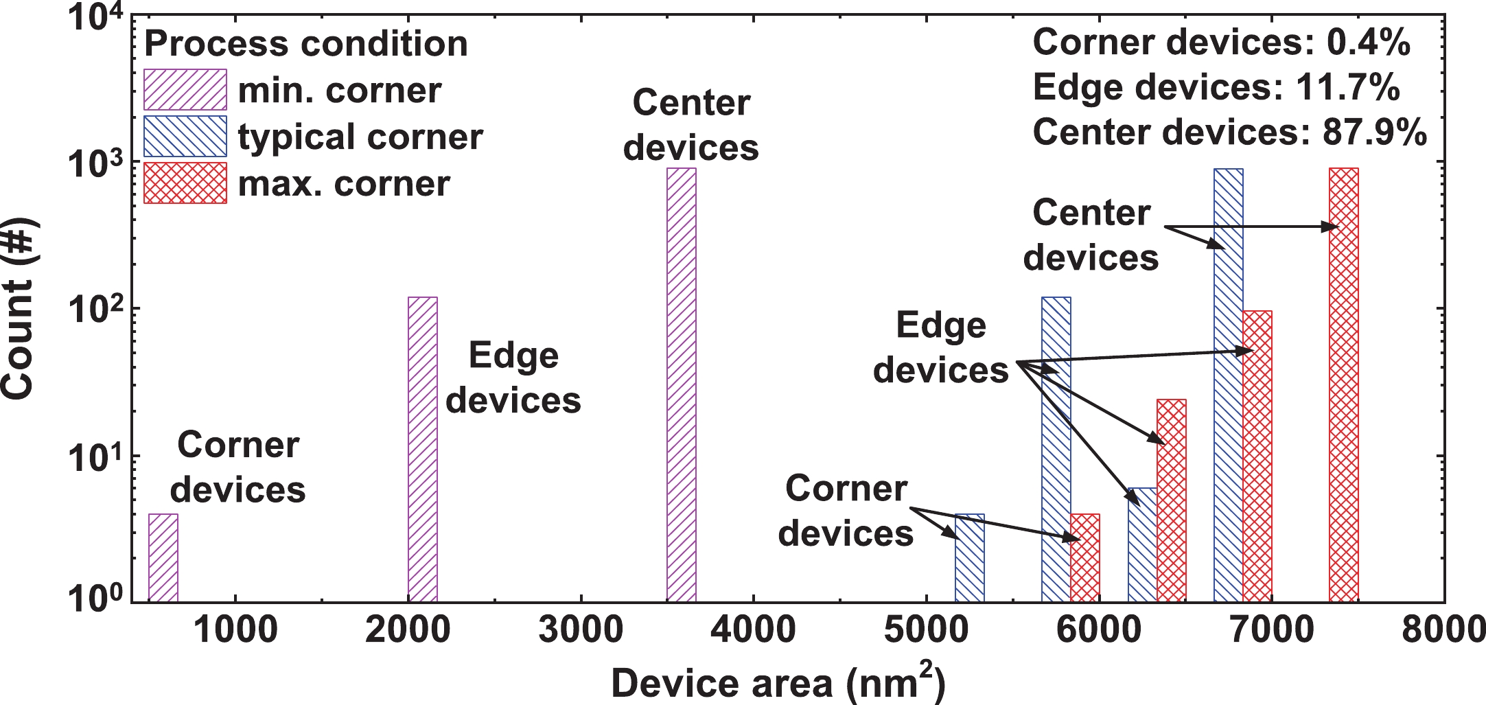
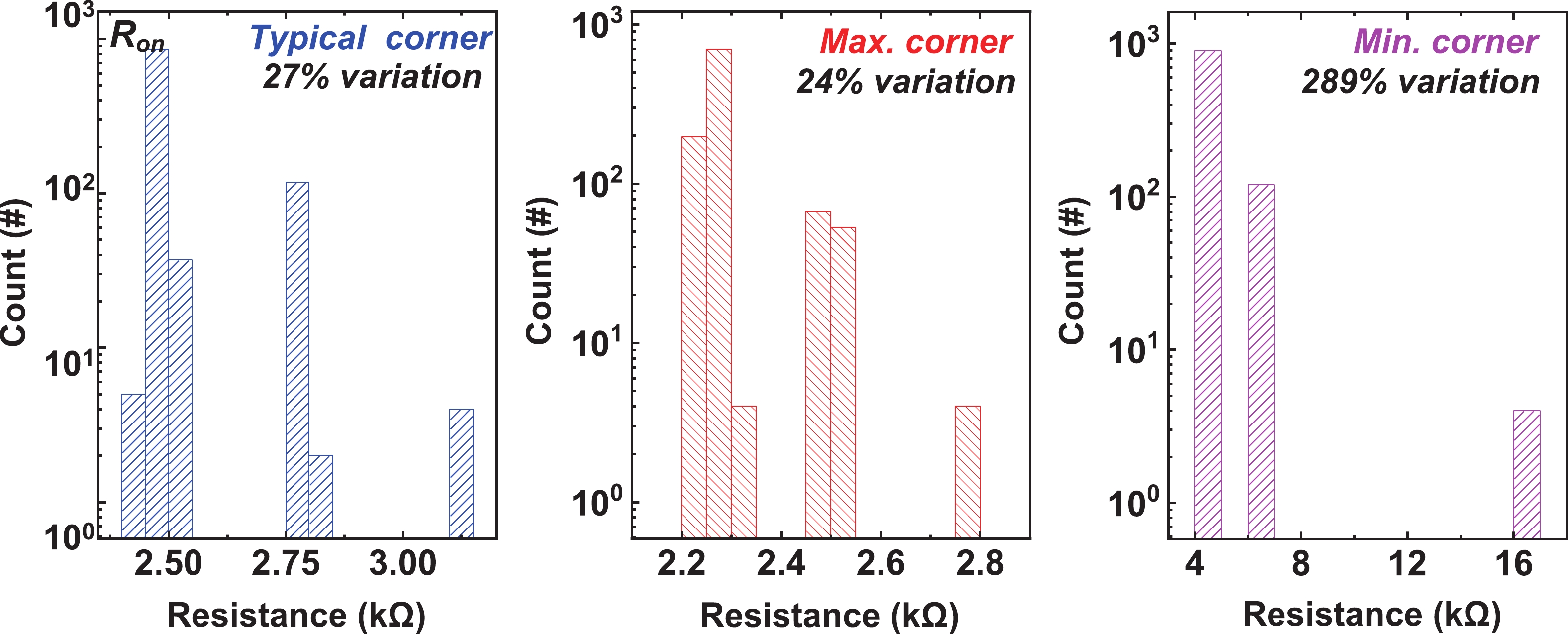
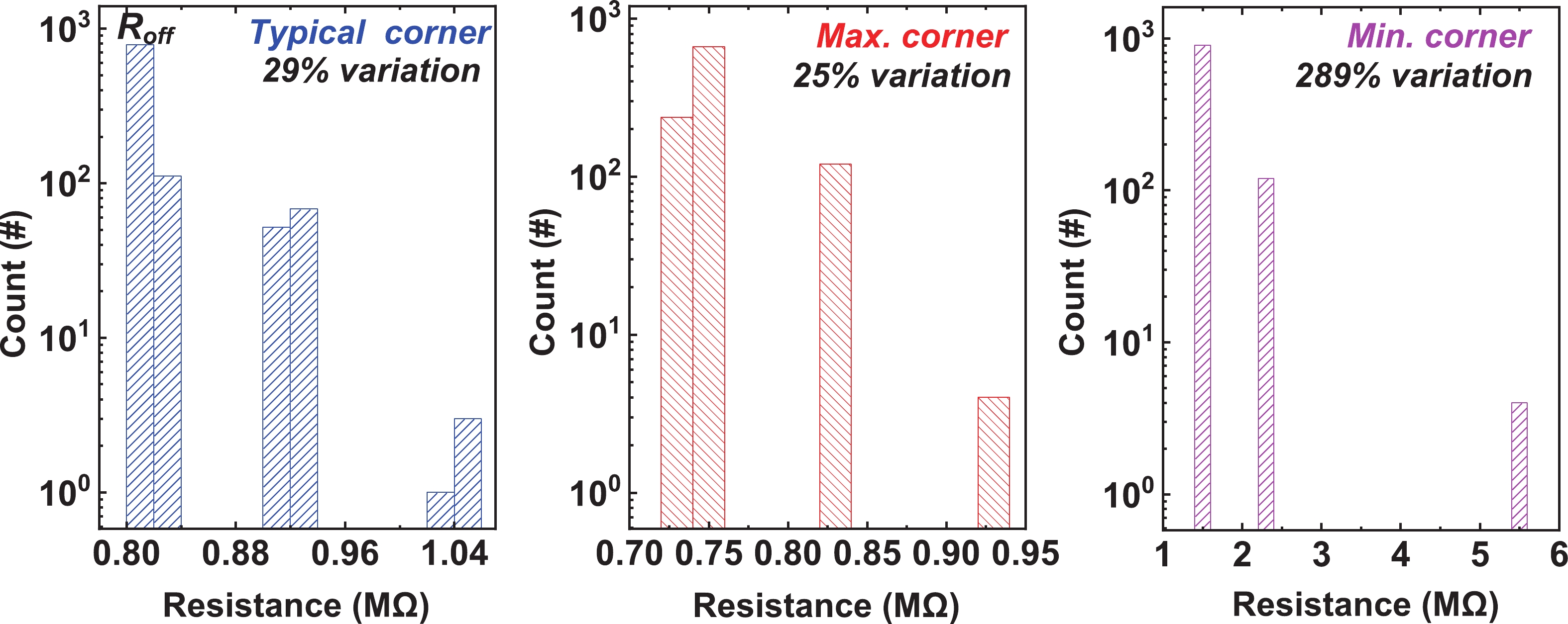
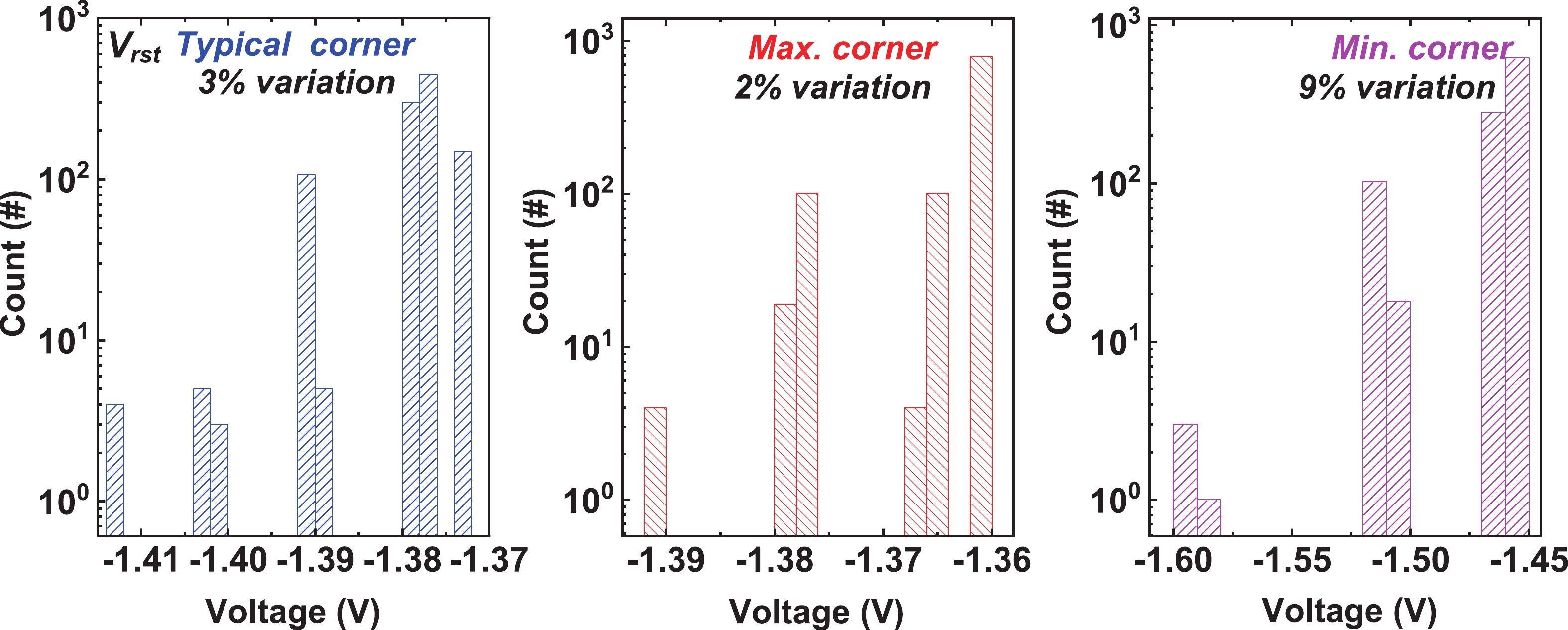
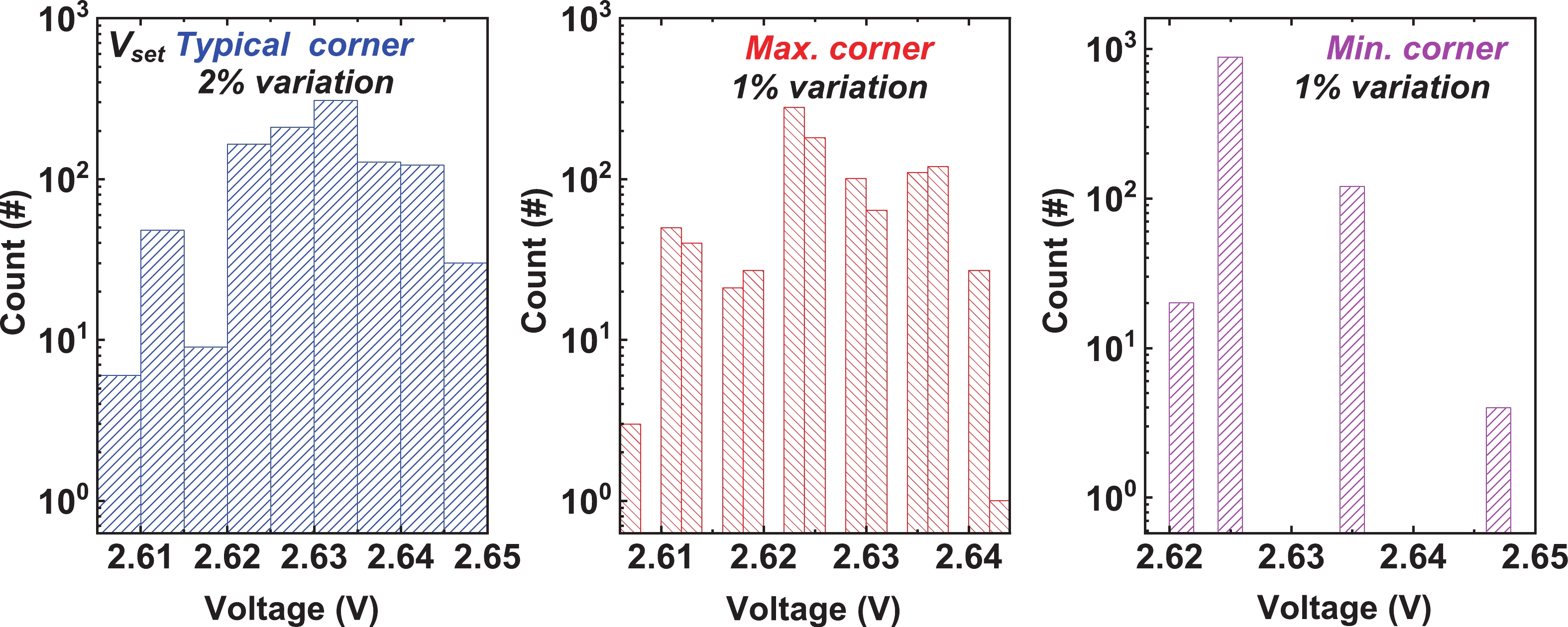
Abstract: Reducing the process variation is a significant concern for resistive random access memory (RRAM). Due to its ultra-high integration density, RRAM arrays are prone to lithographic variation during the lithography process, introducing electrical variation among different RRAM devices. In this work, an optical physical verification methodology for the RRAM array is developed, and the effects of different layout parameters on important electrical characteristics are systematically investigated. The results indicate that the RRAM devices can be categorized into three clusters according to their locations and lithography environments. The read resistance is more sensitive to the locations in the array (~30%) than SET/RESET voltage (<10%). The increase in the RRAM device length and the application of the optical proximity correction technique can help to reduce the variation to less than 10%, whereas it reduces RRAM read resistance by 4×, resulting in a higher power and area consumption. As such, we provide design guidelines to minimize the electrical variation of RRAM arrays due to the lithography process.
Key words: layout, lithography, process variation, resistive random access memory
| [1] |
Tsunoda K, Kinoshita K, Noshiro H, et al. Low power and high speed switching of Ti-doped NiO ReRAM under the unipolar voltage source of less than 3 V. 2007 IEEE International Electron Devices Meeting, 2007, 767 doi: 10.1109/IEDM.2007.4419060
|
| [2] |
Govoreanu B, Kar G S, Chen Y Y, et al. 10 × 10 nm2 Hf/HfO x crossbar resistive RAM with excellent performance, reliability and low-energy operation. 2011 International Electron Devices Meeting, 2011, 31.6. 1 doi: 10.1109/IEDM.2011.6131652
|
| [3] |
Maeda T, Omura Y, Kuroda R, et al. Resistance measurement platform for statistical analysis of emerging memory materials. IEEE Trans Semicond Manuf, 2020, 33, 232 doi: 10.1109/TSM.2020.2983100
|
| [4] |
Xue C X, Huang T Y, Liu J S, et al. 15.4 A 22nm 2Mb ReRAM compute-in-memory macro with 121-28TOPS/W for multibit MAC computing for tiny AI edge devices. 2020 IEEE International Solid-State Circuits Conference - (ISSCC), 2020, 244 doi: 10.1109/ISSCC19947.2020.9063078
|
| [5] |
Shafiee A, Nag A, Muralimanohar N, et al. ISAAC: A convolutional neural network accelerator with In-situ analog arithmetic in crossbars. 2016 ACM/IEEE 43rd Annual International Symposium on Computer Architecture (ISCA), 2016, 14 doi: 10.1109/ISCA.2016.12
|
| [6] |
Zhang Y H, He G H, Tang K T, et al. On-chip learning of multilayer perceptron based on memristors with limited multilevel states. 2019 IEEE International Conference on Artificial Intelligence Circuits and Systems (AICAS), 2019, 11 doi: 10.1109/AICAS.2019.8771513
|
| [7] |
Zhang Y H, He G H, Wang G X, et al. Efficient and robust RRAM-based convolutional weight mapping with shifted and duplicated kernel. IEEE Trans Comput Aided Des Integr Circuits Syst, 2021, 40, 287 doi: 10.1109/TCAD.2020.2998728
|
| [8] |
Xia L X, Liu M Y, Ning X F, et al. Fault-tolerant training enabled by on-line fault detection for RRAM-based neural computing systems. IEEE Trans Comput Aided Des Integr Circuits Syst, 2019, 38, 1611 doi: 10.1109/TCAD.2018.2855145
|
| [9] |
Mostafa H, Ismail Y. Process variation aware design of multi-valued spintronic memristor-based memory arrays. IEEE Trans Semicond Manuf, 2016, 29, 145 doi: 10.1109/TSM.2016.2551224
|
| [10] |
Ma X, Arce G R. Computational Lithography. New York City: Wiley, 2010 doi: 10.1002/9780470618943
|
| [11] |
Maslow M J, Yaegashi H, Frommhold A, et al. Understanding the significance of local variability in defect-aware process windows. IEEE Trans Semicond Manuf, 2020, 33, 42 doi: 10.1109/TSM.2019.2960090
|
| [12] |
Lin Y B, Li M, Watanabe Y, et al. Data efficient lithography modeling with transfer learning and active data selection. IEEE Trans Comput Aided Des Integr Circuits Syst, 2019, 38, 1900 doi: 10.1109/TCAD.2018.2864251
|
| [13] |
Shin C, Park I J. Impact of using double-patterning versus single-patterning on threshold voltage (VTH) variation in quasi-planar tri-gate bulk MOSFETs. IEEE Electron Device Lett, 2013, 34, 578 doi: 10.1109/LED.2013.2249653
|
| [14] |
Huang J J, Wang L L, Lu Y, et al. A highly configurable and extensible spiral capacitor design for high density or high precision applications. 2021 IEEE International Symposium on Circuits and Systems (ISCAS), 2021, 1 doi: 10.1109/ISCAS51556.2021.9401506
|
| [15] |
Choi M, Milor L. Impact on circuit performance of deterministic within-die variation in nanoscale semiconductor manufacturing. IEEE Trans Comput Aided Des Integr Circuits Syst, 2006, 25, 1350 doi: 10.1109/TCAD.2005.855963
|
| [16] |
Chen L, Milor L, Ouyang C, et al. Analysis of the impact of proximity correction algorithms on circuit performance. IEEE Trans Semicond Manuf, 1999, 3, 313 doi: 10.1109/66.778196
|
| [17] |
Yang L M, Song Y L, Liu Y, et al. Linear scaling of reset current down to 22-nm node for a novel Cu xSi yO RRAM. IEEE Electron Device Lett, 2012, 33, 89 doi: 10.1109/LED.2011.2170654
|
| [18] |
Chen Y Y, Goux L, Pantisano L, et al. Scaled X-bar TiN/HfO2/TiN RRAM cells processed with optimized plasma enhanced atomic layer deposition (PEALD) for TiN electrode. Microelectron Eng, 2013, 112, 92 doi: 10.1016/j.mee.2013.02.087
|
| [19] |
Hazra P, Jinesh K B. Scaling of resistive random access memory devices beyond 100 nm2: Influence of grain boundaries studied using scanning tunneling microscopy. Nanotechnology, 2018, 29, 495202 doi: 10.1088/1361-6528/aae17c
|
| [20] |
Long S B, Lian X J, Ye T C, et al. Cycle-to-cycle intrinsic RESET statistics in HfO2-based unipolar RRAM devices. IEEE Electron Device Lett, 2013, 34, 623 doi: 10.1109/LED.2013.2251314
|
| [21] |
Puglisi F M, Larcher L, Padovani A, et al. A complete statistical investigation of RTN in HfO2-based RRAM in high resistive state. IEEE Trans Electron Devices, 2015, 62, 2606 doi: 10.1109/TED.2015.2439812
|
| [22] |
Liu P T, Fan Y S, Chen C C. Improvement of resistive switching uniformity for Al–Zn–Sn–O-based memory device with inserting HfO2 layer. IEEE Electron Device Lett, 2014, 35, 1233 doi: 10.1109/LED.2014.2363491
|
| [23] |
Moulis S, Farys V, Belledent J, et al. A profile-aware resist model with variable threshold. SPIE Photomask Technology. Proc SPIE 8522, Photomask Technology 2012, 2012, 8522, 71 doi: 10.1117/12.966383
|
| [24] |
Granik Y, Cobb N B. New process models for OPC at sub-90-nm nodes. Proceedings of SPIE, 2003, 5040, 1166 doi: 10.1117/12.485321
|
| [25] |
Chen P Y, Yu S M. Compact modeling of RRAM devices and its applications in 1T1R and 1S1R array design. IEEE Trans Electron Devices, 2015, 62, 4022 doi: 10.1109/TED.2015.2492421
|
| [26] |
Lee J, Shin J, Lee D, et al. Diode-less nano-scale ZrO x/HfO x RRAM device with excellent switching uniformity and reliability for high-density cross-point memory applications. 2010 International Electron Devices Meeting, 2010, 19.5. 1 doi: 10.1109/IEDM.2010.5703393
|
| [27] |
Niu D M, Chen Y R, Xu C, et al. Impact of process variations on emerging memristor. Proceedings of the 47th Design Automation Conference. Anaheim California. ACM, 2010, 877 doi: 10.1145/1837274.1837495
|
| [28] |
Wald N, Kvatinsky S. Understanding the influence of device, circuit and environmental variations on real processing in memristive memory using Memristor Aided Logic. Microelectron J, 2019, 86, 22 doi: 10.1016/j.mejo.2019.02.013
|
| [29] |
Hu M, Li H, Chen Y R, et al. Geometry variations analysis of TiO2 thin-film and spintronic memristors. 16th Asia and South Pacific Design Automation Conference (ASP-DAC 2011). Yokohama, Japan. IEEE, 2011, 25 doi: 10.1109/ASPDAC.2011.5722193
|
| [30] |
Li B X, Gu P, Shan Y, et al. RRAM-based analog approximate computing. IEEE Trans Comput Aided Des Integr Circuits Syst, 2015, 34, 1905 doi: 10.1109/TCAD.2015.2445741
|
| [31] |
Aziza H, Ayari H, Onkaraiah S, et al. Oxide based resistive RAM: ON/OFF resistance analysis versus circuit variability. 2014 IEEE International Symposium on Defect and Fault Tolerance in VLSI and Nanotechnology Systems (DFT), 2014, 81 doi: 10.1109/DFT.2014.6962107
|
| [32] |
Aziza H, Bocquet M, Portal J M, et al. Evaluation of OxRAM cell variability impact on memory performances through electrical simulations. 2011 11th Annual Non-Volatile Memory Technology Symposium Proceeding, 2011, 1 doi: 10.1109/NVMTS.2011.6137089
|
| [33] |
Aziza H, Bocquet M, Moreau M, et al. Single-ended sense amplifier robustness evaluation for OxRRAM technology. 2013 8th IEEE Design and Test Symposium, 2013, 1 doi: 10.1109/IDT.2013.6727097
|
| [34] |
Klayout layout viewer and editor, (Date last accessed 23-Feb-2021). [Online]. Available: https://www.klayout.de/
|
| [35] |
Calibre OPCverify user’s and reference manual, Mentor Graphic, 2017.
|
| [36] |
HSPICE user guide: Simulation and analysis, Synopsys, 2013
|
| [37] |
Shen W S, Huang P, Feng Y L, et al. Experimental investigation of the scalability of RRAM device with Pt/[HfO x/AlO y] m/TiN Structure. 2018 14th IEEE International Conference on Solid-State and Integrated Circuit Technology (ICSICT), 2018, 1 doi: 10.1109/ICSICT.2018.8564856
|
| [38] |
Gu A, Zakhor A. Optical proximity correction with linear regression. IEEE Trans Semicond Manuf, 2008, 21, 263 doi: 10.1109/TSM.2008.2000283
|
| [39] |
Calibre OPCpro user’s and reference manual, Mentor Graphic, 2020.
|
| [40] |
Xia L X, Gu P, Li B X, et al. Technological exploration of RRAM crossbar array for matrix-vector multiplication. J Comput Sci Technol, 2016, 31, 3 doi: 10.1007/s11390-016-1608-8
|
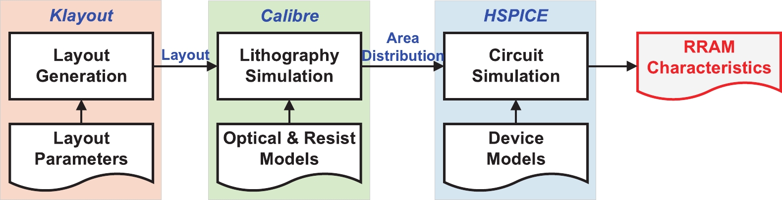
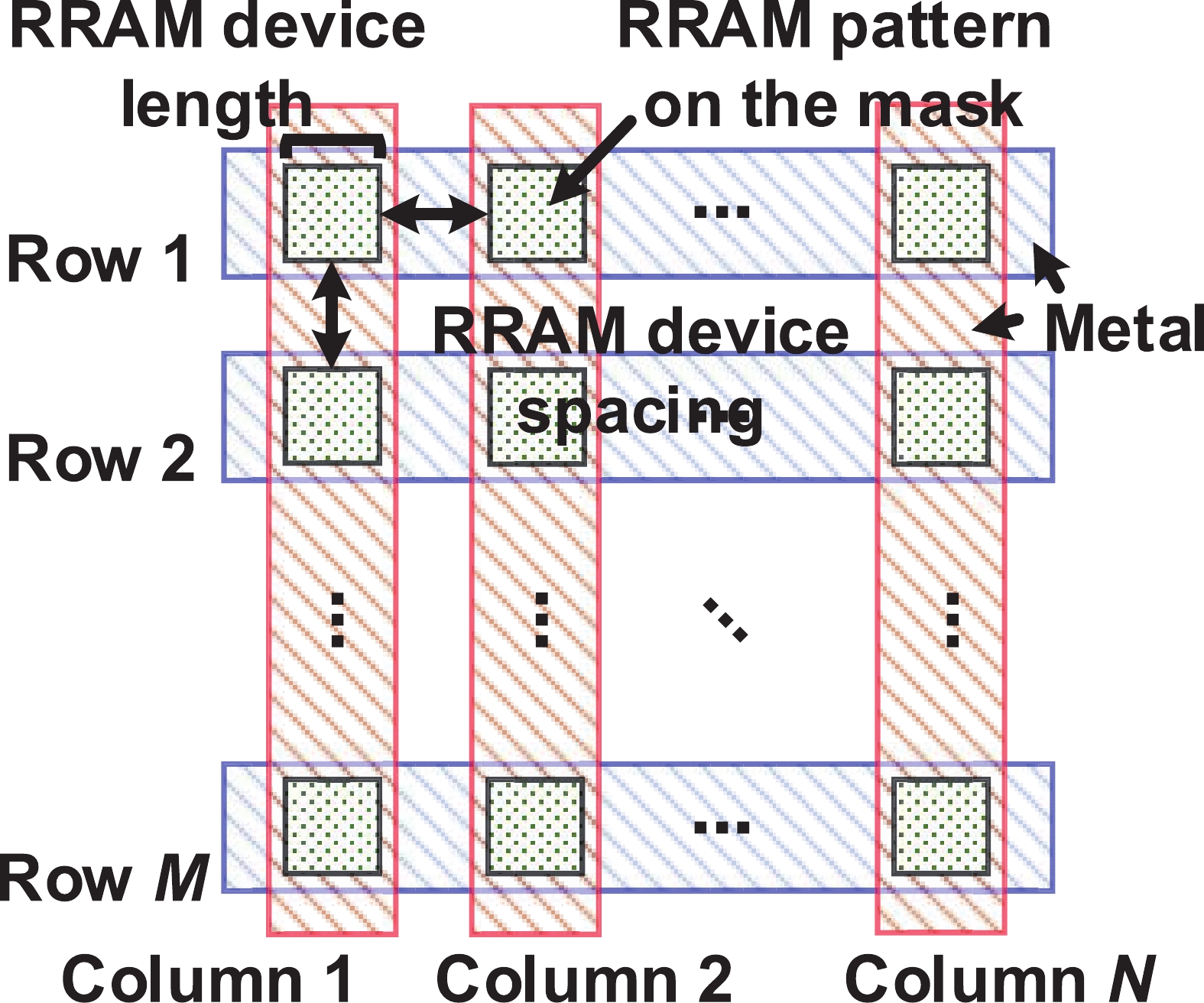
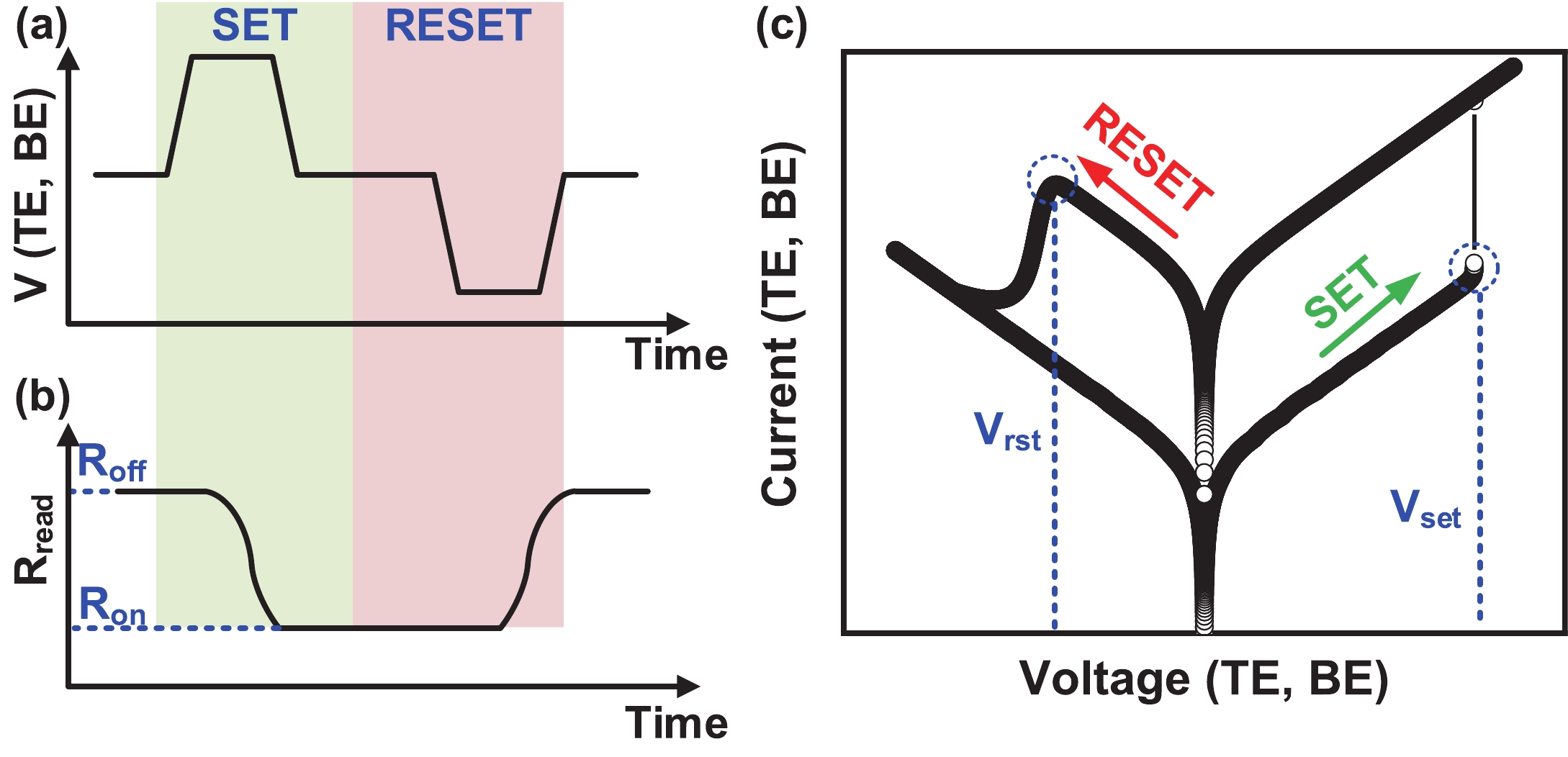
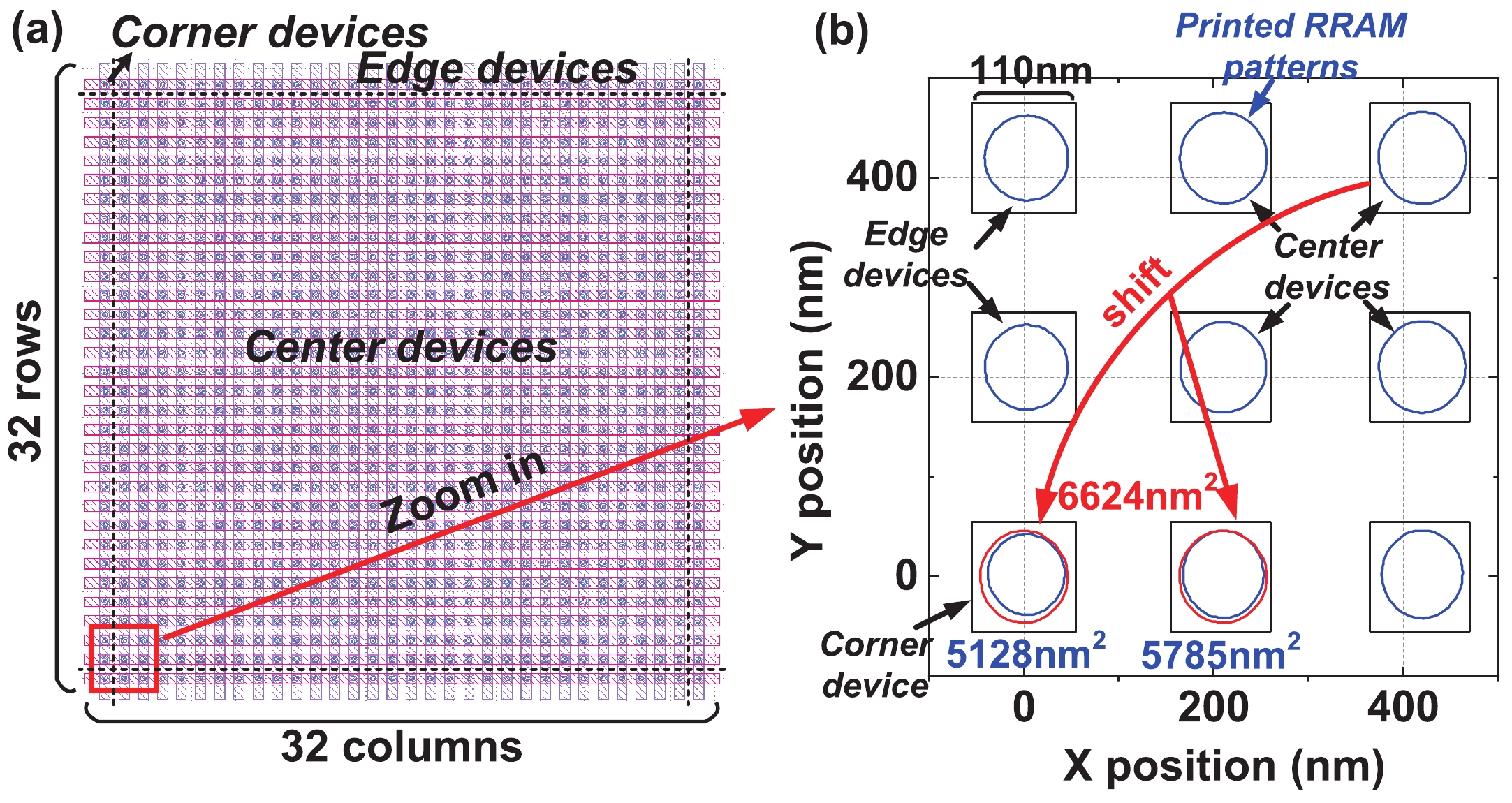
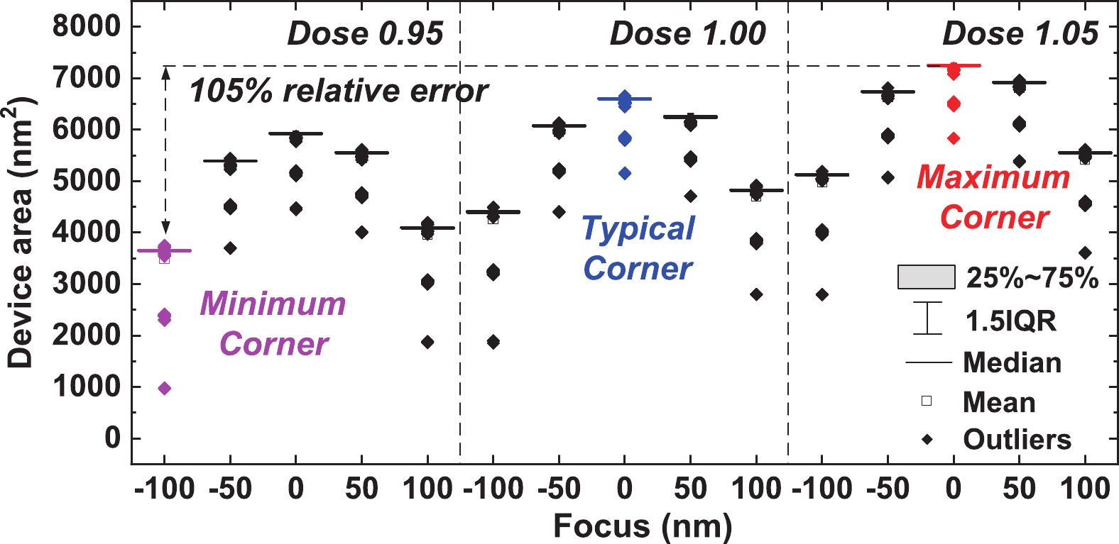
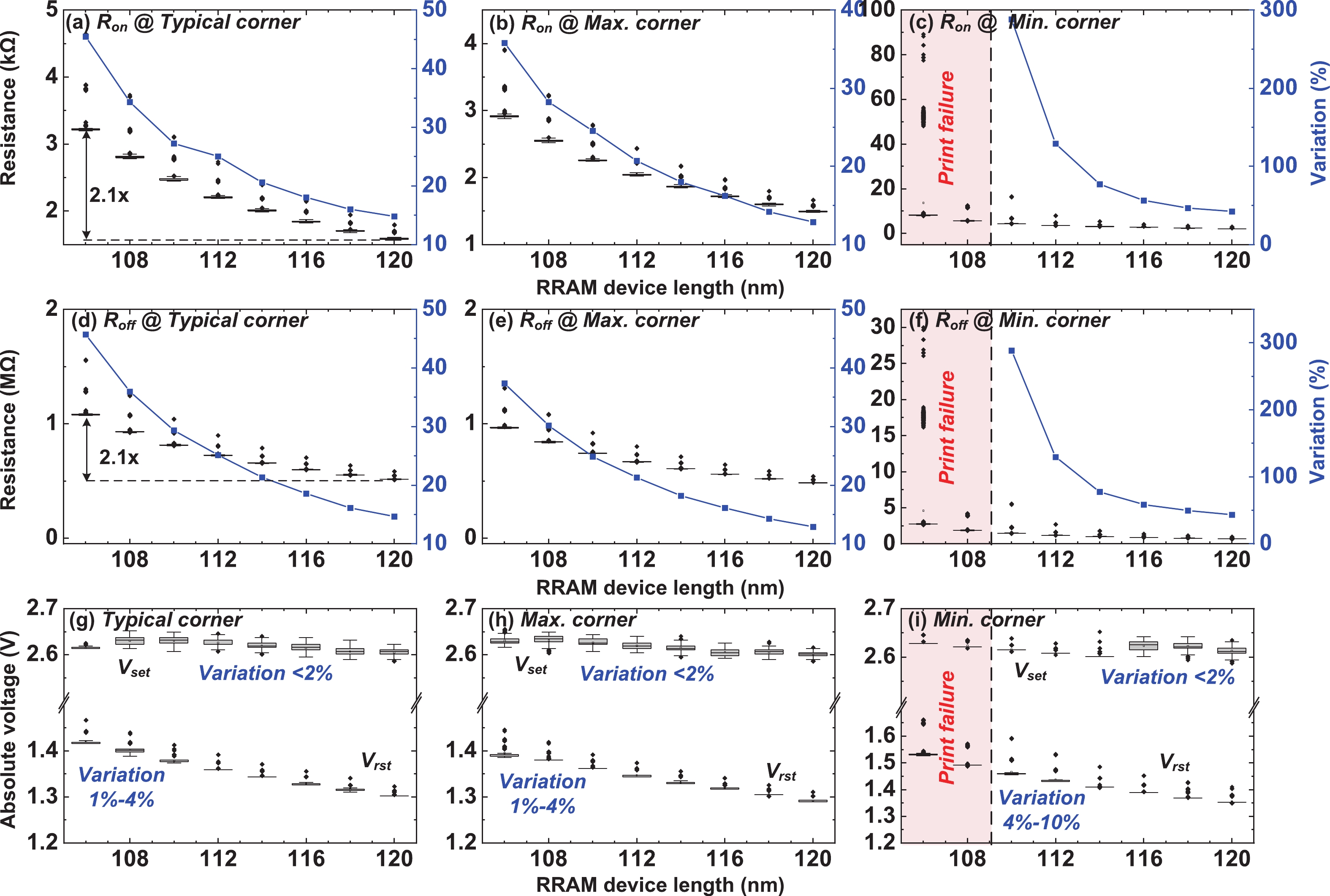
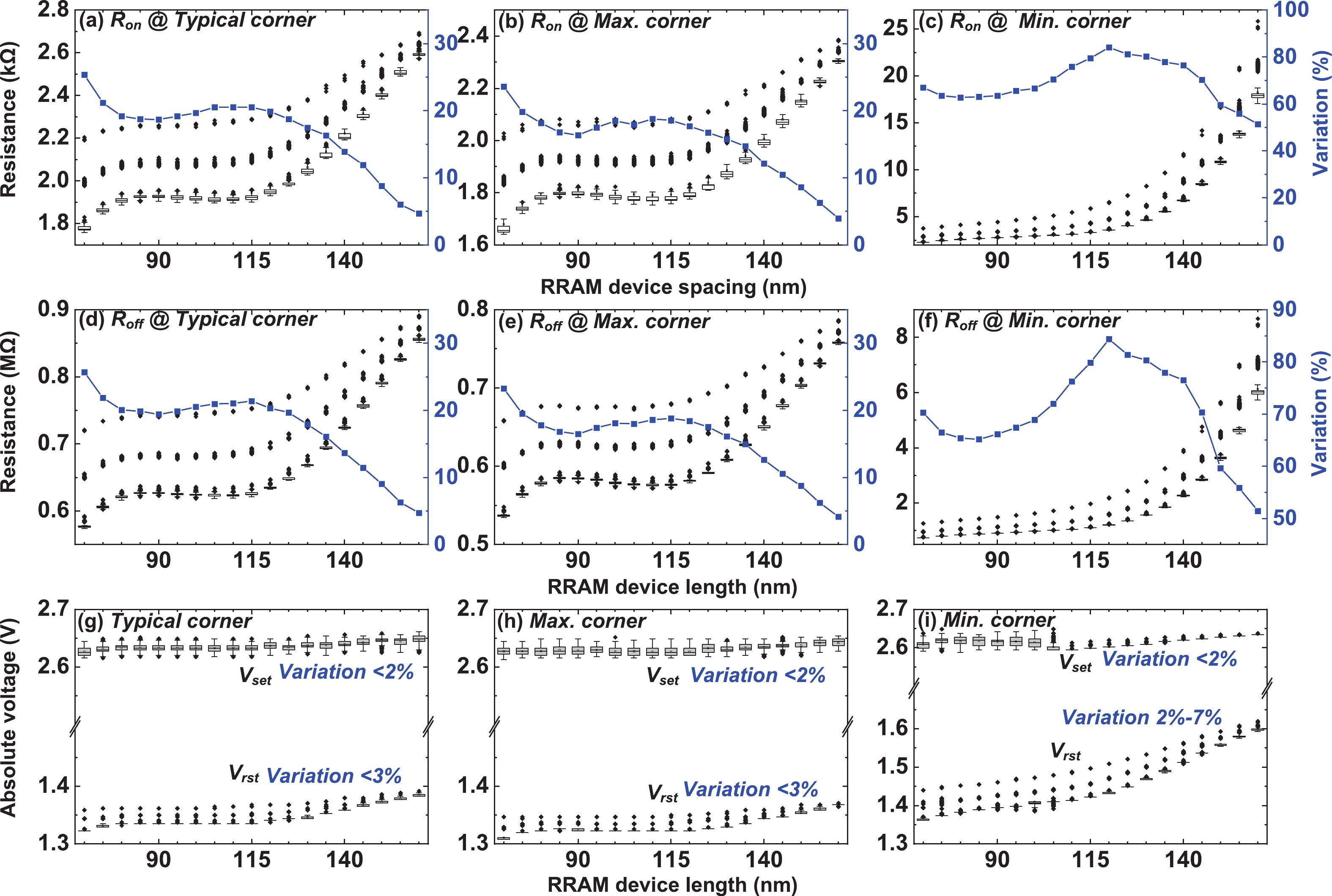
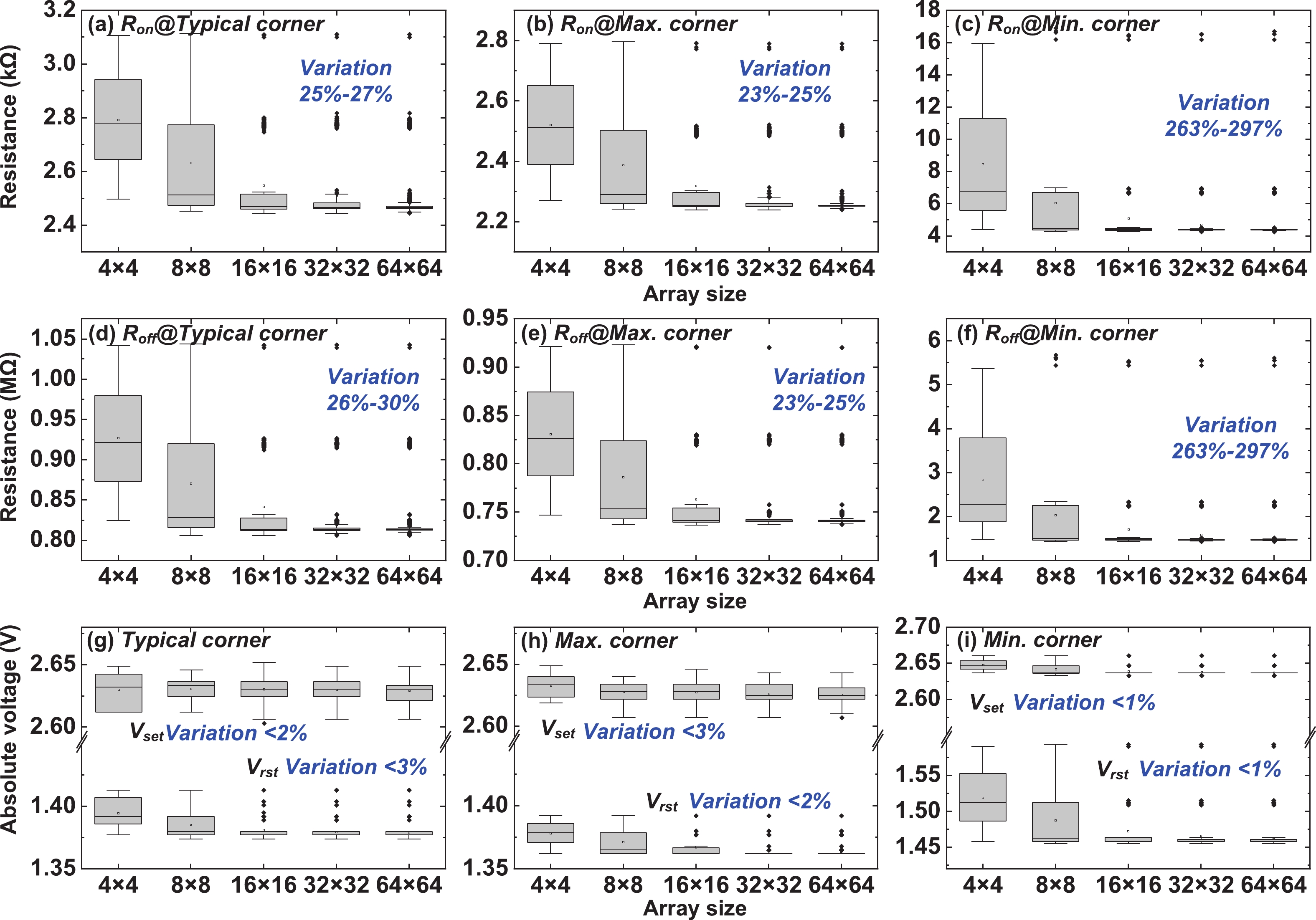
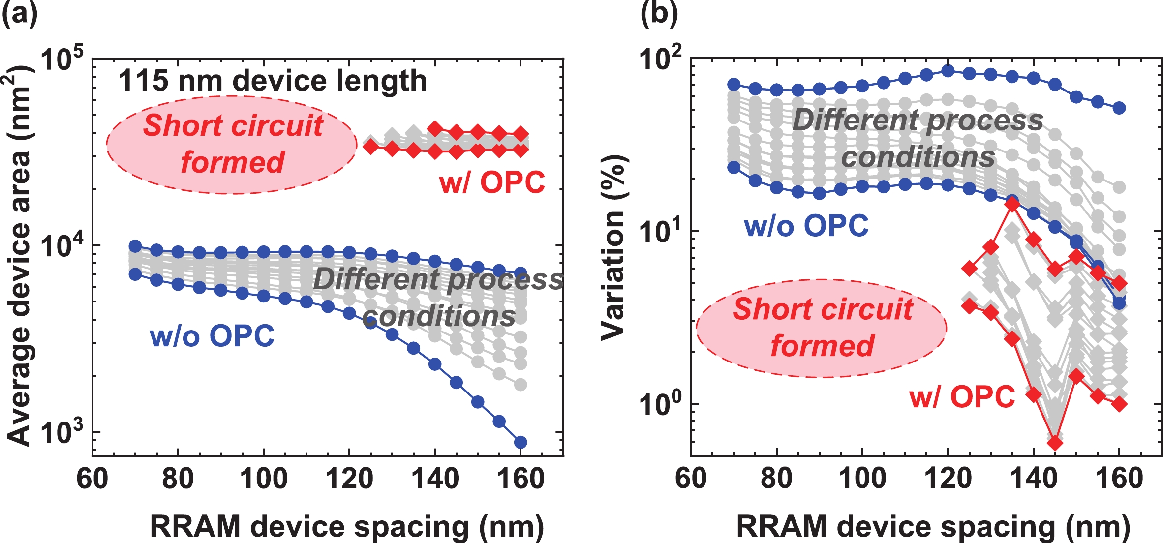
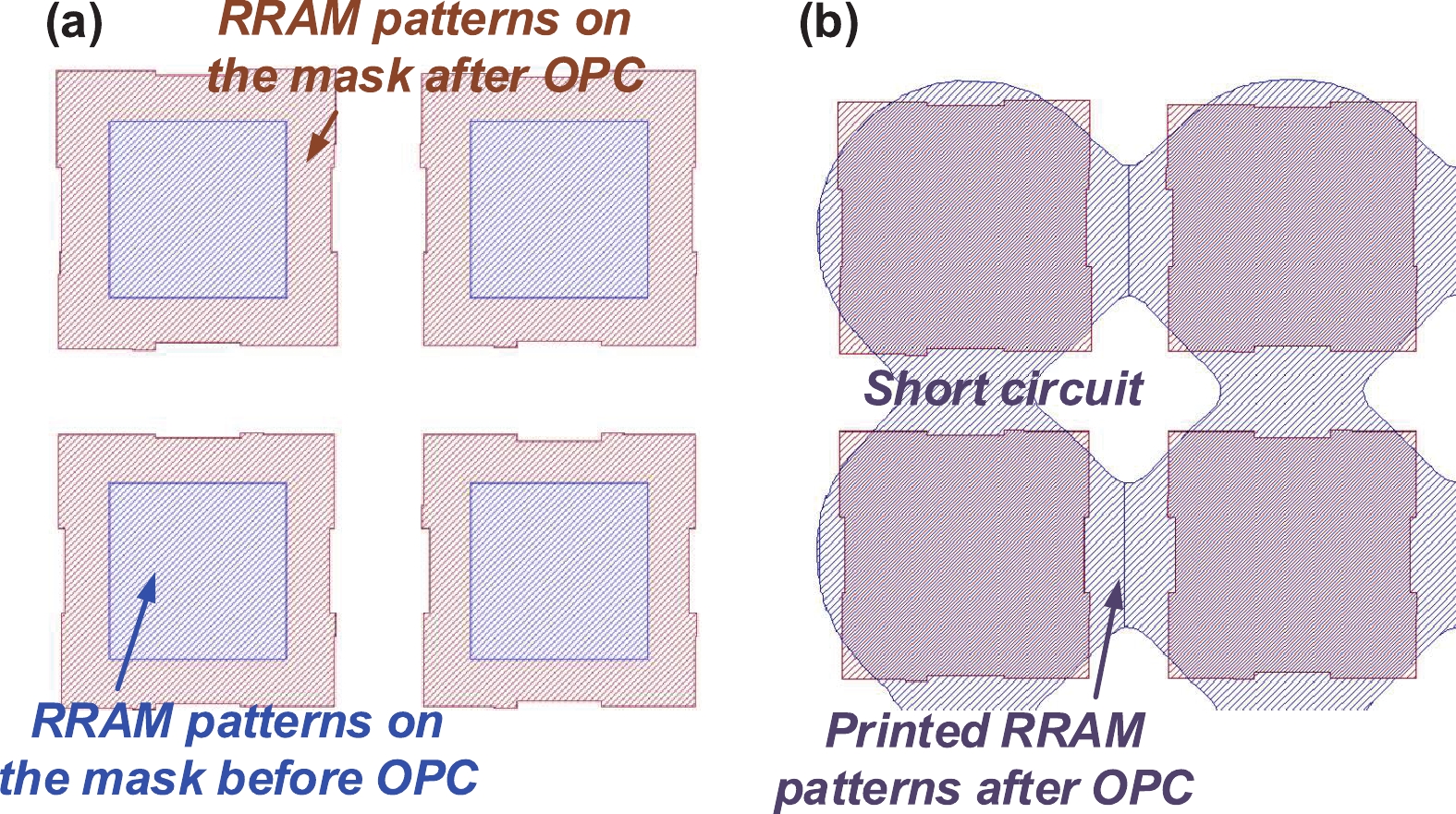
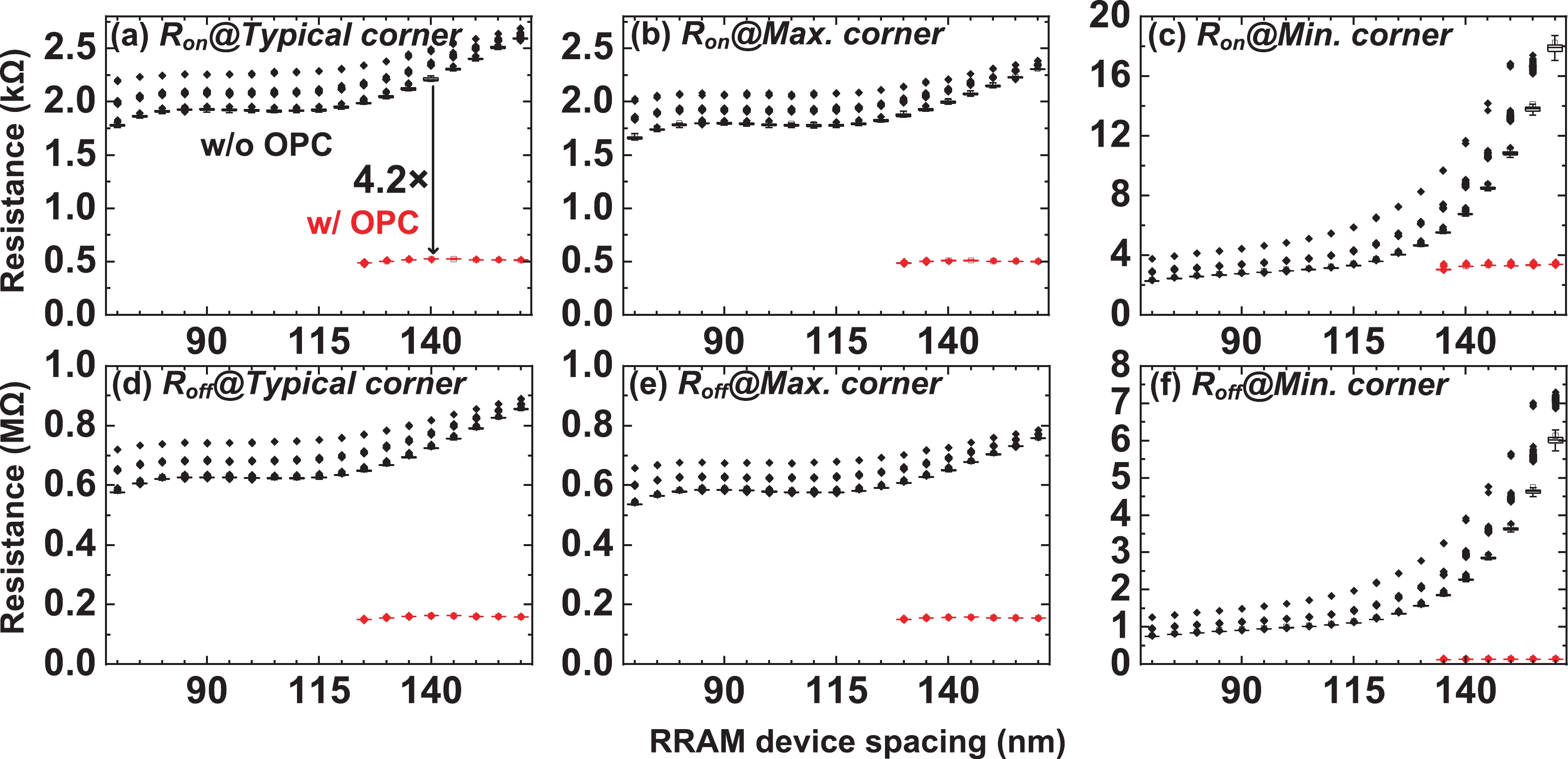
Table 1. RRAM parameter variation before and after OPC applied.
| Variation before OPC | Variation after OPC | ||||||
| Typical corner (%) | Maximum corner (%) | Minimum corner (%) | Typical corner (%) | Maximum corner (%) | Minimum corner (%) | ||
| Ron | 13.9 | 12.2 | 76.5 | 1.7 | 1.8 | 8.4 | |
| Roff | 13.7 | 12.6 | 76.5 | 1.1 | 1.2 | 8.1 | |
| Vset | 1.5 | 1.5 | 0.3 | 0.5 | 0.7 | 0.8 | |
| Vrst | 1.5 | 1.1 | 3.6 | 0.8 | 0.8 | 2.0 | |
 DownLoad: CSV
| [1] |
Tsunoda K, Kinoshita K, Noshiro H, et al. Low power and high speed switching of Ti-doped NiO ReRAM under the unipolar voltage source of less than 3 V. 2007 IEEE International Electron Devices Meeting, 2007, 767 doi: 10.1109/IEDM.2007.4419060
|
| [2] |
Govoreanu B, Kar G S, Chen Y Y, et al. 10 × 10 nm2 Hf/HfO x crossbar resistive RAM with excellent performance, reliability and low-energy operation. 2011 International Electron Devices Meeting, 2011, 31.6. 1 doi: 10.1109/IEDM.2011.6131652
|
| [3] |
Maeda T, Omura Y, Kuroda R, et al. Resistance measurement platform for statistical analysis of emerging memory materials. IEEE Trans Semicond Manuf, 2020, 33, 232 doi: 10.1109/TSM.2020.2983100
|
| [4] |
Xue C X, Huang T Y, Liu J S, et al. 15.4 A 22nm 2Mb ReRAM compute-in-memory macro with 121-28TOPS/W for multibit MAC computing for tiny AI edge devices. 2020 IEEE International Solid-State Circuits Conference - (ISSCC), 2020, 244 doi: 10.1109/ISSCC19947.2020.9063078
|
| [5] |
Shafiee A, Nag A, Muralimanohar N, et al. ISAAC: A convolutional neural network accelerator with In-situ analog arithmetic in crossbars. 2016 ACM/IEEE 43rd Annual International Symposium on Computer Architecture (ISCA), 2016, 14 doi: 10.1109/ISCA.2016.12
|
| [6] |
Zhang Y H, He G H, Tang K T, et al. On-chip learning of multilayer perceptron based on memristors with limited multilevel states. 2019 IEEE International Conference on Artificial Intelligence Circuits and Systems (AICAS), 2019, 11 doi: 10.1109/AICAS.2019.8771513
|
| [7] |
Zhang Y H, He G H, Wang G X, et al. Efficient and robust RRAM-based convolutional weight mapping with shifted and duplicated kernel. IEEE Trans Comput Aided Des Integr Circuits Syst, 2021, 40, 287 doi: 10.1109/TCAD.2020.2998728
|
| [8] |
Xia L X, Liu M Y, Ning X F, et al. Fault-tolerant training enabled by on-line fault detection for RRAM-based neural computing systems. IEEE Trans Comput Aided Des Integr Circuits Syst, 2019, 38, 1611 doi: 10.1109/TCAD.2018.2855145
|
| [9] |
Mostafa H, Ismail Y. Process variation aware design of multi-valued spintronic memristor-based memory arrays. IEEE Trans Semicond Manuf, 2016, 29, 145 doi: 10.1109/TSM.2016.2551224
|
| [10] |
Ma X, Arce G R. Computational Lithography. New York City: Wiley, 2010 doi: 10.1002/9780470618943
|
| [11] |
Maslow M J, Yaegashi H, Frommhold A, et al. Understanding the significance of local variability in defect-aware process windows. IEEE Trans Semicond Manuf, 2020, 33, 42 doi: 10.1109/TSM.2019.2960090
|
| [12] |
Lin Y B, Li M, Watanabe Y, et al. Data efficient lithography modeling with transfer learning and active data selection. IEEE Trans Comput Aided Des Integr Circuits Syst, 2019, 38, 1900 doi: 10.1109/TCAD.2018.2864251
|
| [13] |
Shin C, Park I J. Impact of using double-patterning versus single-patterning on threshold voltage (VTH) variation in quasi-planar tri-gate bulk MOSFETs. IEEE Electron Device Lett, 2013, 34, 578 doi: 10.1109/LED.2013.2249653
|
| [14] |
Huang J J, Wang L L, Lu Y, et al. A highly configurable and extensible spiral capacitor design for high density or high precision applications. 2021 IEEE International Symposium on Circuits and Systems (ISCAS), 2021, 1 doi: 10.1109/ISCAS51556.2021.9401506
|
| [15] |
Choi M, Milor L. Impact on circuit performance of deterministic within-die variation in nanoscale semiconductor manufacturing. IEEE Trans Comput Aided Des Integr Circuits Syst, 2006, 25, 1350 doi: 10.1109/TCAD.2005.855963
|
| [16] |
Chen L, Milor L, Ouyang C, et al. Analysis of the impact of proximity correction algorithms on circuit performance. IEEE Trans Semicond Manuf, 1999, 3, 313 doi: 10.1109/66.778196
|
| [17] |
Yang L M, Song Y L, Liu Y, et al. Linear scaling of reset current down to 22-nm node for a novel Cu xSi yO RRAM. IEEE Electron Device Lett, 2012, 33, 89 doi: 10.1109/LED.2011.2170654
|
| [18] |
Chen Y Y, Goux L, Pantisano L, et al. Scaled X-bar TiN/HfO2/TiN RRAM cells processed with optimized plasma enhanced atomic layer deposition (PEALD) for TiN electrode. Microelectron Eng, 2013, 112, 92 doi: 10.1016/j.mee.2013.02.087
|
| [19] |
Hazra P, Jinesh K B. Scaling of resistive random access memory devices beyond 100 nm2: Influence of grain boundaries studied using scanning tunneling microscopy. Nanotechnology, 2018, 29, 495202 doi: 10.1088/1361-6528/aae17c
|
| [20] |
Long S B, Lian X J, Ye T C, et al. Cycle-to-cycle intrinsic RESET statistics in HfO2-based unipolar RRAM devices. IEEE Electron Device Lett, 2013, 34, 623 doi: 10.1109/LED.2013.2251314
|
| [21] |
Puglisi F M, Larcher L, Padovani A, et al. A complete statistical investigation of RTN in HfO2-based RRAM in high resistive state. IEEE Trans Electron Devices, 2015, 62, 2606 doi: 10.1109/TED.2015.2439812
|
| [22] |
Liu P T, Fan Y S, Chen C C. Improvement of resistive switching uniformity for Al–Zn–Sn–O-based memory device with inserting HfO2 layer. IEEE Electron Device Lett, 2014, 35, 1233 doi: 10.1109/LED.2014.2363491
|
| [23] |
Moulis S, Farys V, Belledent J, et al. A profile-aware resist model with variable threshold. SPIE Photomask Technology. Proc SPIE 8522, Photomask Technology 2012, 2012, 8522, 71 doi: 10.1117/12.966383
|
| [24] |
Granik Y, Cobb N B. New process models for OPC at sub-90-nm nodes. Proceedings of SPIE, 2003, 5040, 1166 doi: 10.1117/12.485321
|
| [25] |
Chen P Y, Yu S M. Compact modeling of RRAM devices and its applications in 1T1R and 1S1R array design. IEEE Trans Electron Devices, 2015, 62, 4022 doi: 10.1109/TED.2015.2492421
|
| [26] |
Lee J, Shin J, Lee D, et al. Diode-less nano-scale ZrO x/HfO x RRAM device with excellent switching uniformity and reliability for high-density cross-point memory applications. 2010 International Electron Devices Meeting, 2010, 19.5. 1 doi: 10.1109/IEDM.2010.5703393
|
| [27] |
Niu D M, Chen Y R, Xu C, et al. Impact of process variations on emerging memristor. Proceedings of the 47th Design Automation Conference. Anaheim California. ACM, 2010, 877 doi: 10.1145/1837274.1837495
|
| [28] |
Wald N, Kvatinsky S. Understanding the influence of device, circuit and environmental variations on real processing in memristive memory using Memristor Aided Logic. Microelectron J, 2019, 86, 22 doi: 10.1016/j.mejo.2019.02.013
|
| [29] |
Hu M, Li H, Chen Y R, et al. Geometry variations analysis of TiO2 thin-film and spintronic memristors. 16th Asia and South Pacific Design Automation Conference (ASP-DAC 2011). Yokohama, Japan. IEEE, 2011, 25 doi: 10.1109/ASPDAC.2011.5722193
|
| [30] |
Li B X, Gu P, Shan Y, et al. RRAM-based analog approximate computing. IEEE Trans Comput Aided Des Integr Circuits Syst, 2015, 34, 1905 doi: 10.1109/TCAD.2015.2445741
|
| [31] |
Aziza H, Ayari H, Onkaraiah S, et al. Oxide based resistive RAM: ON/OFF resistance analysis versus circuit variability. 2014 IEEE International Symposium on Defect and Fault Tolerance in VLSI and Nanotechnology Systems (DFT), 2014, 81 doi: 10.1109/DFT.2014.6962107
|
| [32] |
Aziza H, Bocquet M, Portal J M, et al. Evaluation of OxRAM cell variability impact on memory performances through electrical simulations. 2011 11th Annual Non-Volatile Memory Technology Symposium Proceeding, 2011, 1 doi: 10.1109/NVMTS.2011.6137089
|
| [33] |
Aziza H, Bocquet M, Moreau M, et al. Single-ended sense amplifier robustness evaluation for OxRRAM technology. 2013 8th IEEE Design and Test Symposium, 2013, 1 doi: 10.1109/IDT.2013.6727097
|
| [34] |
Klayout layout viewer and editor, (Date last accessed 23-Feb-2021). [Online]. Available: https://www.klayout.de/
|
| [35] |
Calibre OPCverify user’s and reference manual, Mentor Graphic, 2017.
|
| [36] |
HSPICE user guide: Simulation and analysis, Synopsys, 2013
|
| [37] |
Shen W S, Huang P, Feng Y L, et al. Experimental investigation of the scalability of RRAM device with Pt/[HfO x/AlO y] m/TiN Structure. 2018 14th IEEE International Conference on Solid-State and Integrated Circuit Technology (ICSICT), 2018, 1 doi: 10.1109/ICSICT.2018.8564856
|
| [38] |
Gu A, Zakhor A. Optical proximity correction with linear regression. IEEE Trans Semicond Manuf, 2008, 21, 263 doi: 10.1109/TSM.2008.2000283
|
| [39] |
Calibre OPCpro user’s and reference manual, Mentor Graphic, 2020.
|
| [40] |
Xia L X, Gu P, Li B X, et al. Technological exploration of RRAM crossbar array for matrix-vector multiplication. J Comput Sci Technol, 2016, 31, 3 doi: 10.1007/s11390-016-1608-8
|


Article views: 190 Times PDF downloads: 34 Times Cited by: 0 Times
Received: 13 December 2023 Revised: 26 January 2024 Online: Accepted Manuscript: 01 March 2024Uncorrected proof: 08 March 2024Published: 10 May 2024
| Citation: |
Yuhang Zhang, Guanghui He, Feng Zhang, Yongfu Li, Guoxing Wang. The study of lithographic variation in resistive random access memory[J]. Journal of Semiconductors, 2024, 45(5): 052303. doi: 10.1088/1674-4926/45/5/052303
Y H Zhang, G H He, F Zhang, Y F Li, and G X Wang, The study of lithographic variation in resistive random access memory[J]. J. Semicond., 2024, 45(5), 052303 doi: 10.1088/1674-4926/45/5/052303
Export: BibTex EndNote

|
| [1] |
Tsunoda K, Kinoshita K, Noshiro H, et al. Low power and high speed switching of Ti-doped NiO ReRAM under the unipolar voltage source of less than 3 V. 2007 IEEE International Electron Devices Meeting, 2007, 767 doi: 10.1109/IEDM.2007.4419060
|
| [2] |
Govoreanu B, Kar G S, Chen Y Y, et al. 10 × 10 nm2 Hf/HfO x crossbar resistive RAM with excellent performance, reliability and low-energy operation. 2011 International Electron Devices Meeting, 2011, 31.6. 1 doi: 10.1109/IEDM.2011.6131652
|
| [3] |
Maeda T, Omura Y, Kuroda R, et al. Resistance measurement platform for statistical analysis of emerging memory materials. IEEE Trans Semicond Manuf, 2020, 33, 232 doi: 10.1109/TSM.2020.2983100
|
| [4] |
Xue C X, Huang T Y, Liu J S, et al. 15.4 A 22nm 2Mb ReRAM compute-in-memory macro with 121-28TOPS/W for multibit MAC computing for tiny AI edge devices. 2020 IEEE International Solid-State Circuits Conference - (ISSCC), 2020, 244 doi: 10.1109/ISSCC19947.2020.9063078
|
| [5] |
Shafiee A, Nag A, Muralimanohar N, et al. ISAAC: A convolutional neural network accelerator with In-situ analog arithmetic in crossbars. 2016 ACM/IEEE 43rd Annual International Symposium on Computer Architecture (ISCA), 2016, 14 doi: 10.1109/ISCA.2016.12
|
| [6] |
Zhang Y H, He G H, Tang K T, et al. On-chip learning of multilayer perceptron based on memristors with limited multilevel states. 2019 IEEE International Conference on Artificial Intelligence Circuits and Systems (AICAS), 2019, 11 doi: 10.1109/AICAS.2019.8771513
|
| [7] |
Zhang Y H, He G H, Wang G X, et al. Efficient and robust RRAM-based convolutional weight mapping with shifted and duplicated kernel. IEEE Trans Comput Aided Des Integr Circuits Syst, 2021, 40, 287 doi: 10.1109/TCAD.2020.2998728
|
| [8] |
Xia L X, Liu M Y, Ning X F, et al. Fault-tolerant training enabled by on-line fault detection for RRAM-based neural computing systems. IEEE Trans Comput Aided Des Integr Circuits Syst, 2019, 38, 1611 doi: 10.1109/TCAD.2018.2855145
|
| [9] |
Mostafa H, Ismail Y. Process variation aware design of multi-valued spintronic memristor-based memory arrays. IEEE Trans Semicond Manuf, 2016, 29, 145 doi: 10.1109/TSM.2016.2551224
|
| [10] |
Ma X, Arce G R. Computational Lithography. New York City: Wiley, 2010 doi: 10.1002/9780470618943
|
| [11] |
Maslow M J, Yaegashi H, Frommhold A, et al. Understanding the significance of local variability in defect-aware process windows. IEEE Trans Semicond Manuf, 2020, 33, 42 doi: 10.1109/TSM.2019.2960090
|
| [12] |
Lin Y B, Li M, Watanabe Y, et al. Data efficient lithography modeling with transfer learning and active data selection. IEEE Trans Comput Aided Des Integr Circuits Syst, 2019, 38, 1900 doi: 10.1109/TCAD.2018.2864251
|
| [13] |
Shin C, Park I J. Impact of using double-patterning versus single-patterning on threshold voltage (VTH) variation in quasi-planar tri-gate bulk MOSFETs. IEEE Electron Device Lett, 2013, 34, 578 doi: 10.1109/LED.2013.2249653
|
| [14] |
Huang J J, Wang L L, Lu Y, et al. A highly configurable and extensible spiral capacitor design for high density or high precision applications. 2021 IEEE International Symposium on Circuits and Systems (ISCAS), 2021, 1 doi: 10.1109/ISCAS51556.2021.9401506
|
| [15] |
Choi M, Milor L. Impact on circuit performance of deterministic within-die variation in nanoscale semiconductor manufacturing. IEEE Trans Comput Aided Des Integr Circuits Syst, 2006, 25, 1350 doi: 10.1109/TCAD.2005.855963
|
| [16] |
Chen L, Milor L, Ouyang C, et al. Analysis of the impact of proximity correction algorithms on circuit performance. IEEE Trans Semicond Manuf, 1999, 3, 313 doi: 10.1109/66.778196
|
| [17] |
Yang L M, Song Y L, Liu Y, et al. Linear scaling of reset current down to 22-nm node for a novel Cu xSi yO RRAM. IEEE Electron Device Lett, 2012, 33, 89 doi: 10.1109/LED.2011.2170654
|
| [18] |
Chen Y Y, Goux L, Pantisano L, et al. Scaled X-bar TiN/HfO2/TiN RRAM cells processed with optimized plasma enhanced atomic layer deposition (PEALD) for TiN electrode. Microelectron Eng, 2013, 112, 92 doi: 10.1016/j.mee.2013.02.087
|
| [19] |
Hazra P, Jinesh K B. Scaling of resistive random access memory devices beyond 100 nm2: Influence of grain boundaries studied using scanning tunneling microscopy. Nanotechnology, 2018, 29, 495202 doi: 10.1088/1361-6528/aae17c
|
| [20] |
Long S B, Lian X J, Ye T C, et al. Cycle-to-cycle intrinsic RESET statistics in HfO2-based unipolar RRAM devices. IEEE Electron Device Lett, 2013, 34, 623 doi: 10.1109/LED.2013.2251314
|
| [21] |
Puglisi F M, Larcher L, Padovani A, et al. A complete statistical investigation of RTN in HfO2-based RRAM in high resistive state. IEEE Trans Electron Devices, 2015, 62, 2606 doi: 10.1109/TED.2015.2439812
|
| [22] |
Liu P T, Fan Y S, Chen C C. Improvement of resistive switching uniformity for Al–Zn–Sn–O-based memory device with inserting HfO2 layer. IEEE Electron Device Lett, 2014, 35, 1233 doi: 10.1109/LED.2014.2363491
|
| [23] |
Moulis S, Farys V, Belledent J, et al. A profile-aware resist model with variable threshold. SPIE Photomask Technology. Proc SPIE 8522, Photomask Technology 2012, 2012, 8522, 71 doi: 10.1117/12.966383
|
| [24] |
Granik Y, Cobb N B. New process models for OPC at sub-90-nm nodes. Proceedings of SPIE, 2003, 5040, 1166 doi: 10.1117/12.485321
|
| [25] |
Chen P Y, Yu S M. Compact modeling of RRAM devices and its applications in 1T1R and 1S1R array design. IEEE Trans Electron Devices, 2015, 62, 4022 doi: 10.1109/TED.2015.2492421
|
| [26] |
Lee J, Shin J, Lee D, et al. Diode-less nano-scale ZrO x/HfO x RRAM device with excellent switching uniformity and reliability for high-density cross-point memory applications. 2010 International Electron Devices Meeting, 2010, 19.5. 1 doi: 10.1109/IEDM.2010.5703393
|
| [27] |
Niu D M, Chen Y R, Xu C, et al. Impact of process variations on emerging memristor. Proceedings of the 47th Design Automation Conference. Anaheim California. ACM, 2010, 877 doi: 10.1145/1837274.1837495
|
| [28] |
Wald N, Kvatinsky S. Understanding the influence of device, circuit and environmental variations on real processing in memristive memory using Memristor Aided Logic. Microelectron J, 2019, 86, 22 doi: 10.1016/j.mejo.2019.02.013
|
| [29] |
Hu M, Li H, Chen Y R, et al. Geometry variations analysis of TiO2 thin-film and spintronic memristors. 16th Asia and South Pacific Design Automation Conference (ASP-DAC 2011). Yokohama, Japan. IEEE, 2011, 25 doi: 10.1109/ASPDAC.2011.5722193
|
| [30] |
Li B X, Gu P, Shan Y, et al. RRAM-based analog approximate computing. IEEE Trans Comput Aided Des Integr Circuits Syst, 2015, 34, 1905 doi: 10.1109/TCAD.2015.2445741
|
| [31] |
Aziza H, Ayari H, Onkaraiah S, et al. Oxide based resistive RAM: ON/OFF resistance analysis versus circuit variability. 2014 IEEE International Symposium on Defect and Fault Tolerance in VLSI and Nanotechnology Systems (DFT), 2014, 81 doi: 10.1109/DFT.2014.6962107
|
| [32] |
Aziza H, Bocquet M, Portal J M, et al. Evaluation of OxRAM cell variability impact on memory performances through electrical simulations. 2011 11th Annual Non-Volatile Memory Technology Symposium Proceeding, 2011, 1 doi: 10.1109/NVMTS.2011.6137089
|
| [33] |
Aziza H, Bocquet M, Moreau M, et al. Single-ended sense amplifier robustness evaluation for OxRRAM technology. 2013 8th IEEE Design and Test Symposium, 2013, 1 doi: 10.1109/IDT.2013.6727097
|
| [34] |
Klayout layout viewer and editor, (Date last accessed 23-Feb-2021). [Online]. Available: https://www.klayout.de/
|
| [35] |
Calibre OPCverify user’s and reference manual, Mentor Graphic, 2017.
|
| [36] |
HSPICE user guide: Simulation and analysis, Synopsys, 2013
|
| [37] |
Shen W S, Huang P, Feng Y L, et al. Experimental investigation of the scalability of RRAM device with Pt/[HfO x/AlO y] m/TiN Structure. 2018 14th IEEE International Conference on Solid-State and Integrated Circuit Technology (ICSICT), 2018, 1 doi: 10.1109/ICSICT.2018.8564856
|
| [38] |
Gu A, Zakhor A. Optical proximity correction with linear regression. IEEE Trans Semicond Manuf, 2008, 21, 263 doi: 10.1109/TSM.2008.2000283
|
| [39] |
Calibre OPCpro user’s and reference manual, Mentor Graphic, 2020.
|
| [40] |
Xia L X, Gu P, Li B X, et al. Technological exploration of RRAM crossbar array for matrix-vector multiplication. J Comput Sci Technol, 2016, 31, 3 doi: 10.1007/s11390-016-1608-8
|

 WeChat ID
Journal of Semiconductors © 2017 All Rights Reserved 京ICP备05085259号-2