ARTICLES

Dual-Schottky-junctions coupling device based on ultra-long β-Ga2O3 single-crystal nanobelt and its photoelectric properties

Haifeng Chen1, , Xiaocong Han1, Chenlu Wu1, Zhanhang Liu1, Shaoqing Wang1, Xiangtai Liu1, Qin Lu1, Yifan Jia1, Zhan Wang1, Yunhe Guan1, Lijun Li1 and Yue Hao2

+ Author Affiliations

 Corresponding author: Haifeng Chen, chenhaifeng@xupt.edu.cn

PDF

Turn off MathJax

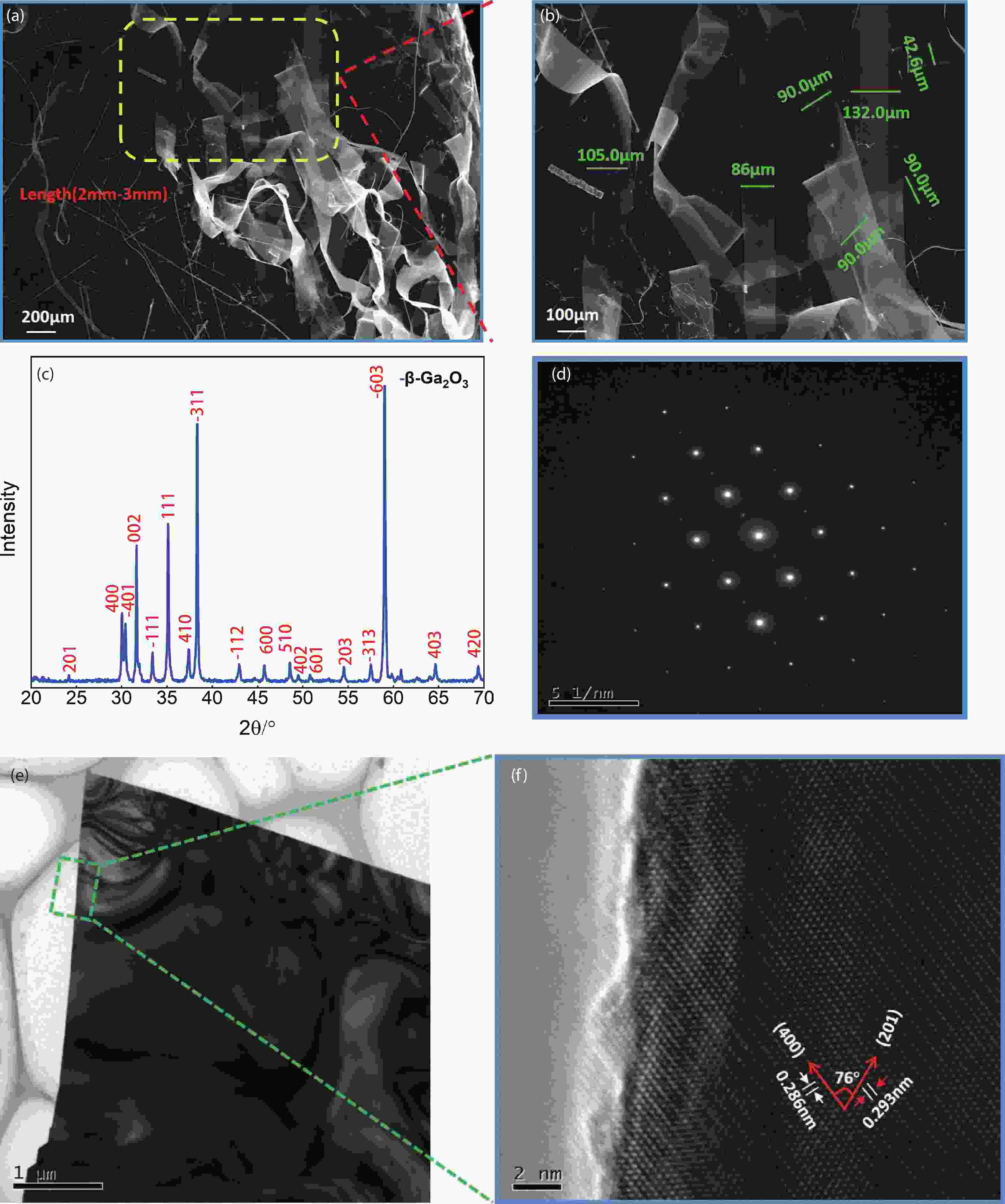
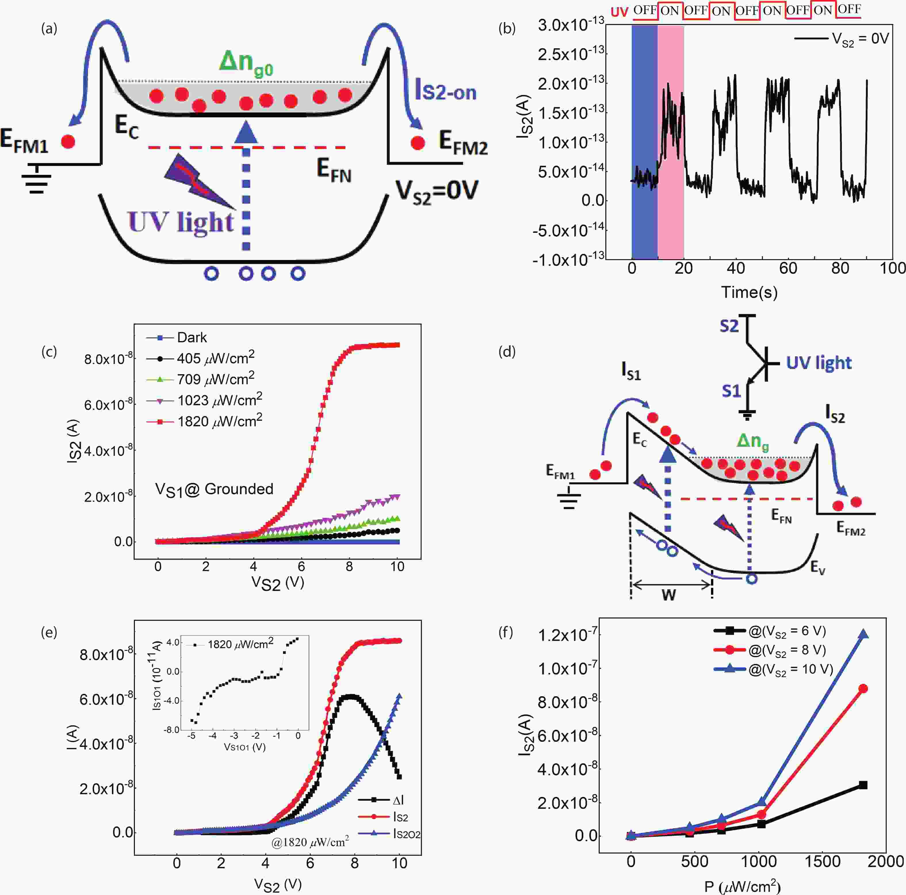
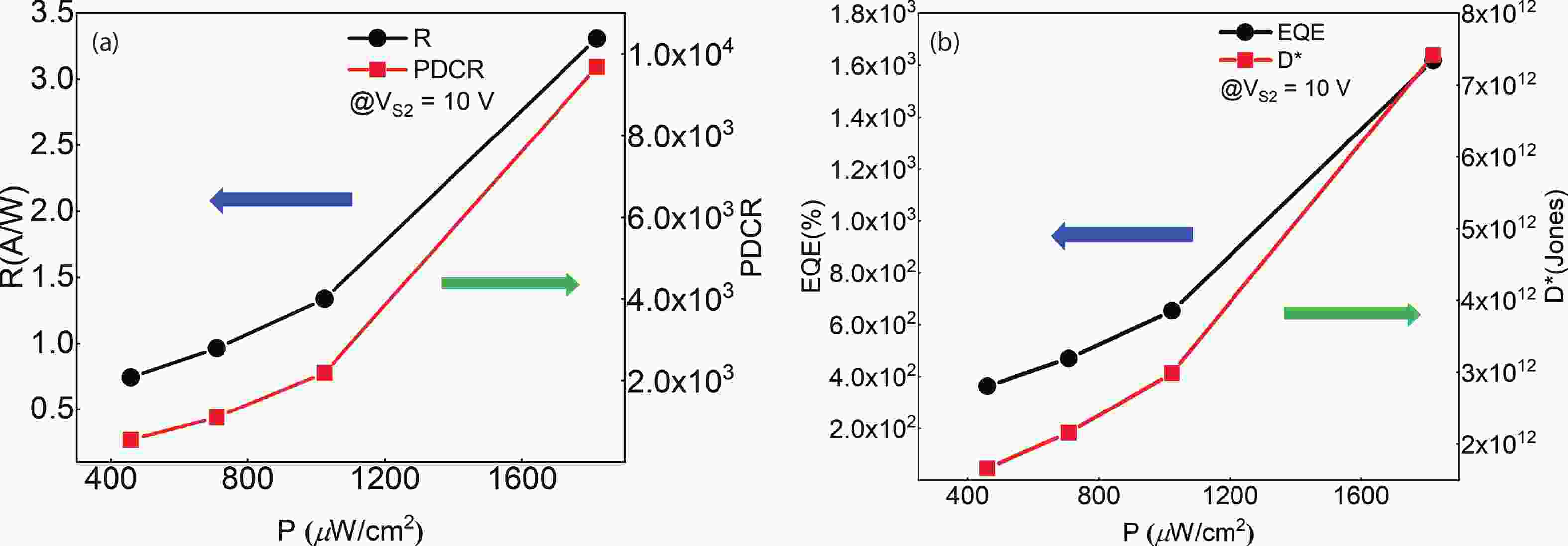
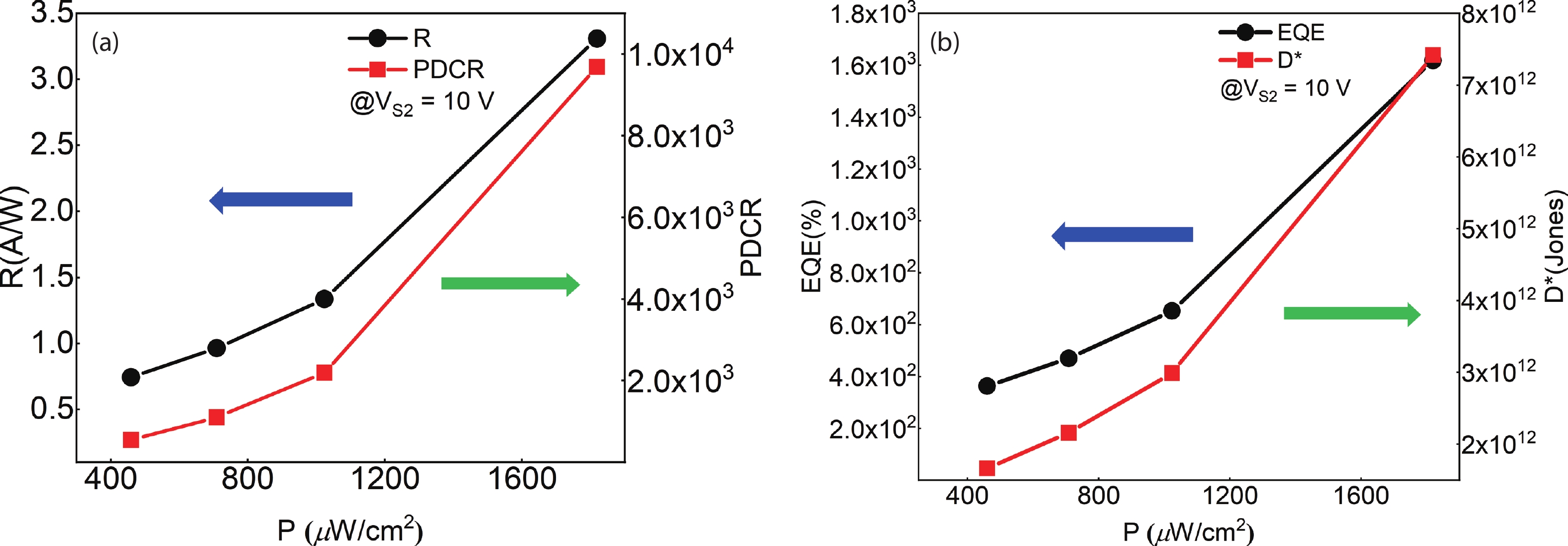
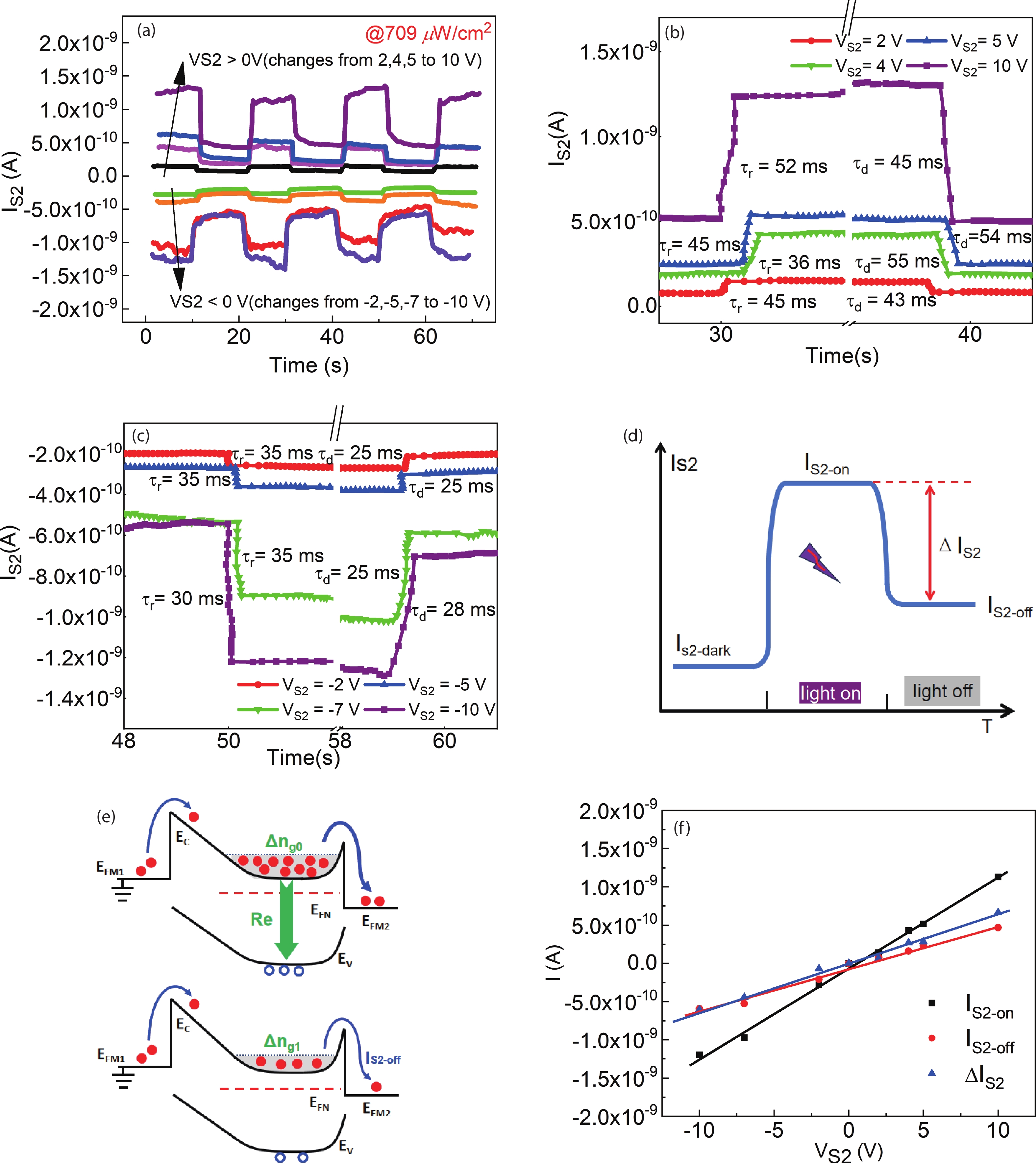
Abstract: High quality β-Ga2O3 single crystal nanobelts with length of 2−3 mm and width from tens of microns to 132 μm were synthesized by carbothermal reduction method. Based on the grown nanobelt with the length of 600 μm, the dual-Schottky-junctions coupling device (DSCD) was fabricated. Due to the electrically floating Ga2O3 nanobelt region coupling with the double Schottky-junctions, the current IS2 increases firstly and rapidly reaches into saturation as increase the voltage VS2. The saturation current is about 10 pA, which is two orders of magnitude lower than that of a single Schottky-junction. In the case of solar-blind ultraviolet (UV) light irradiation, the photogenerated electrons further aggravate the coupling physical mechanism in device. IS2 increases as the intensity of UV light increases. Under the UV light of 1820 μW/cm2, IS2 quickly enters the saturation state. At VS2 = 10 V, photo-to-dark current ratio (PDCR) of the device reaches more than 104, the external quantum efficiency (EQE) is 1.6 × 10³%, and the detectivity (D*) is 7.5 × 10¹² Jones. In addition, the device has a very short rise and decay times of 25−54 ms under different positive and negative bias. DSCD shows unique electrical and optical control characteristics, which will open a new way for the application of nanobelt-based devices.

Key words: β-Ga2O3 nanobeltcarbothermal reductionUV lightdual-Schottky coupling device


[1]
Stepanov S I, Nikolaev V I, Bougrov V E, et al. Gallium oxide: Properties and applications-A review. Rev Adv Mater Sci, 2016, 44, 63
[2]
Higashiwaki M, Murakami H, Kumagai Y, et al. Current status of Ga2O3 power devices. Jpn J Appl Phys, 2016, 55, 1202A1 doi: 10.7567/JJAP.55.1202A1
[3]
Higashiwaki M, Sasaki K, Murakami H, et al. Recent progress in Ga2O3 power devices. Semicond Sci Technol, 2016, 31, 034001 doi: 10.1088/0268-1242/31/3/034001
[4]
Yadav M K, Mondal A, Sharma S K, et al. Substrate orientation dependent current transport mechanisms in β-Ga2O3/Si based Schottky barrier diodes. J Vac Sci Technol A Vac Surf Films, 2021, 39, 033203 doi: 10.1116/6.0000858
[5]
Wang Y B, Xu W H, You T G, et al. β-Ga2O3 MOSFETs on the Si substrate fabricated by the ion-cutting process. Sci China Phys Mech Astron, 2020, 63, 277311 doi: 10.1007/s11433-020-1533-0
[6]
Zhou H, Si M W, Alghamdi S, et al. High-performance depletion/enhancement-ode β-Ga2O3 on insulator (GOOI) field-effect transistors with record drain currents of 600/450 mA/mm. IEEE Electron Device Lett, 2017, 38, 103 doi: 10.1109/LED.2016.2635579
[7]
Yadav M K, Mondal A, Shringi S, et al. Performance enhancement of β-Ga2O3 on Si(100) based Schottky barrier diodes using reduced surface field. Semicond Sci Technol, 2020, 35, 085009 doi: 10.1088/1361-6641/ab8e64
[8]
Abdullah Q N, Ahmed A R, Ali A M, et al. Novel SnO2-coated β-Ga2O3 nanostructures for room temperature hydrogen gas sensor. Int J Hydrog Energy, 2021, 46, 7000 doi: 10.1016/j.ijhydene.2020.11.109
[9]
Liu Z, Li P G, Zhi Y S, et al. Review of gallium oxide based field-effect transistors and Schottky barrier diodes. Chin Phys B, 2019, 28, 017105 doi: 10.1088/1674-1056/28/1/017105
[10]
Guo D Y, Chen K, Wang S L, et al. Self-powered solar-blind photodetectors based on α/β phase junction of Ga2O3. Phys Rev Appl, 2020, 13, 024051 doi: 10.1103/PhysRevApplied.13.024051
[11]
Qin Y, Li L H, Zhao X L, et al. Metal–semiconductor–metal ε-Ga2O3 solar-blind photodetectors with a record-high responsivity rejection ratio and their gain mechanism. ACS Photonics, 2020, 7, 812 doi: 10.1021/acsphotonics.9b01727
[12]
Xiang X Q, Li L H, Chen C, et al. Unintentional doping effect in Si-doped MOCVD β-Ga2O3 films: Shallow donor states. Sci China Mater, 2023, 66, 748 doi: 10.1007/s40843-022-2167-x
[13]
Li L, Auer E, Liao M Y, et al. Deep-ultraviolet solar-blind photoconductivity of individual gallium oxide nanobelts. Nanoscale, 2011, 3, 1120 doi: 10.1039/c0nr00702a
[14]
Zhao B, Wang F, Chen H Y, et al. An ultrahigh responsivity (9.7 mA W–1) self-powered solar-blind photodetector based on individual ZnO–Ga2O3 heterostructures. Adv Funct Materials, 2017, 27, 1700264 doi: 10.1002/adfm.201700264
[15]
Kaur D, Kumar M. A strategic review on gallium oxide based deep-ultraviolet photodetectors: Recent progress and future prospects. Adv Opt Mater, 2021, 9, 2002160 doi: 10.1002/adom.202002160
[16]
Weng W Y, Hsueh T J, Chang S J, et al. A solar-blind β-Ga2O3 nanowire photodetector. IEEE Photonics Technol Lett, 2010, 22, 709 doi: 10.1109/LPT.2010.2044570
[17]
Wu Y L, Chang S J, Weng W Y, et al. Ga2O3 nanowire photodetector prepared on SiO2/Si template. IEEE Sens J, 2013, 13, 2368 doi: 10.1109/JSEN.2013.2247996
[18]
Oh S, Kim J, Ren F, et al. Quasi-two-dimensional β-gallium oxide solar-blind photodetectors with ultrahigh responsivity. J Mater Chem C, 2016, 4, 9245 doi: 10.1039/C6TC02467J
[19]
Suzuki R, Nakagomi S, Kokubun Y, et al. Enhancement of responsivity in solar-blind β-Ga2O3 photodiodes with a Au Schottky contact fabricated on single crystal substrates by annealing. Appl Phys Lett, 2009, 94, 222102 doi: 10.1063/1.3147197
[20]
Chen X, Liu K W, Zhang Z Z, et al. Self-powered solar-blind photodetector with fast response based on Au/β-Ga2O3 nanowires array film Schottky-junction. ACS Appl Mater Interfaces, 2016, 8, 4185 doi: 10.1021/acsami.5b11956
[21]
Kim S, Kim J. Highly selective ozone-treated β-Ga2O3 solar-blind deep-UV photodetectors. Appl Phys Lett, 2020, 117, 261101 doi: 10.1063/5.0030400
[22]
Zhang Y B, Zheng J, Ma P P, et al. Growth and characterization of β-Ga2O3 thin films grown on off-angled Al2O3 substrates by metal-organic chemical vapor deposition. J Semicond, 2022, 43, 092801 doi: 10.1088/1674-4926/43/9/092801
[23]
Qi Q, Chen H F, Hong Z F, et al. Preparation and characteristics of ultra-wide Ga2O3 nanoribbons up to millimeter-long level without catalyst. Acta Phys Sin, 2020, 69, 168101 doi: 10.7498/aps.69.20200481
[24]
Shih H Y, Chu F C, Das A, et al. Atomic layer deposition of gallium oxide films as gate dielectrics in AlGaN/GaN metal-oxide-semiconductor high-electron-mobility transistors. Nanoscale Res Lett, 2016, 11, 235 doi: 10.1186/s11671-016-1448-z
[25]
Wu C, Wu F M, Hu H Z, et al. Review of self-powered solar-blind photodetectors based on Ga2O3. Mater Today Phys, 2022, 28, 100883 doi: 10.1016/j.mtphys.2022.100883
[26]
Kumar A, Bag A. High responsivity of quasi-2D electrospun β-Ga2O3-based deep-UV photodetectors. IEEE Photonics Technol Lett, 2019, 31, 619 doi: 10.1109/LPT.2019.2901236
[27]
He H L, Wu C, Hu H Z, et al. Bandgap engineering and oxygen vacancy defect electroactivity inhibition in highly crystalline N-alloyed Ga2O3 films through plasma-enhanced technology. J Phys Chem Lett, 2023, 14, 6444 doi: 10.1021/acs.jpclett.3c01368
[28]
Cheng Y X, Ye J H, Lai L, et al. Ambipolarity regulation of deep-UV photocurrent by controlling crystalline phases in Ga2O3 nanostructure for switchable logic applications. Adv Elect Materials, 2023, 9, 2201216 doi: 10.1002/aelm.202201216
[29]
Wang Z P, Gong H H, Yu X X, et al. Trap-mediated bipolar charge transport in NiO/Ga2O3 p+-n heterojunction power diodes. Sci China Mater, 2022, 66, 1157 doi: 10.1007/s40843-022-2244-y
[30]
Li Y Q, Zhang D, Jia L M, et al. Ultrawide-bandgap (6.14 eV) (AlGa)2O3/Ga2O3 heterostructure designed by lattice matching strategy for highly sensitive vacuum ultraviolet photodetection. Sci China Mater, 2021, 64, 3027 doi: 10.1007/s40843-021-1698-3
[31]
Chen R R, Wang D, Feng B, et al. High responsivity self-powered DUV photodetectors based on β-Ga2O3/GaN heterogeneous PN junctions. Vacuum, 2023, 215, 112332 doi: 10.1016/j.vacuum.2023.112332
[32]
Bielecki Z, Achtenberg K, Kopytko M, et al. Review of photodetectors characterization methods. Bull Pol Acad Sci Tech Sci, 2022, 70, 144608 doi: 10.24425/bpasts.2022.140534
[33]
Wang D, Ma X C, Chen R R, et al. Solar-blind ultraviolet photodetectors based on Ta-doped β-Ga2O3 heteroepitaxial films. Opt Mater, 2022, 129, 112491 doi: 10.1016/j.optmat.2022.112491
[34]
Vasudevan A, Jung S, Ji T, et al. Quasi-symmetric Wheatstone bridge zinc oxide nanorod UV detectors. IEEE Sens J, 2014, 14, 3310 doi: 10.1109/JSEN.2014.2328871
[35]
Liu N S, Fang G J, Zeng W, et al. Direct growth of lateral ZnO nanorod UV photodetectors with Schottky contact by a single-step hydrothermal reaction. ACS Appl Mater Interfaces, 2010, 2, 1973 doi: 10.1021/am100277q
[36]
Sheoran H, Fang S, Liang F Z, et al. High performance of zero-power-consumption MOCVD-grown β-Ga2O3-based solar-blind photodetectors with ultralow dark current and high-temperature functionalities. ACS Appl Mater Interfaces, 2022, 14, 52096 doi: 10.1021/acsami.2c08511
Fig. 1.  (Color online) (a) SEM diagram of synthesized ultra-large nanobelts which are about 2−3 mm in length. (b) The enlargement of the yellow dotted box of (a). Maximum width of these nanobelts is up to 132 μm. (c) XRD pattern of nanobelt. (d) Electron diffraction patterns of selected regions. (e) Low-resolution TEM image of nanobelt. (f) High resolution TEM image of nanobelt.

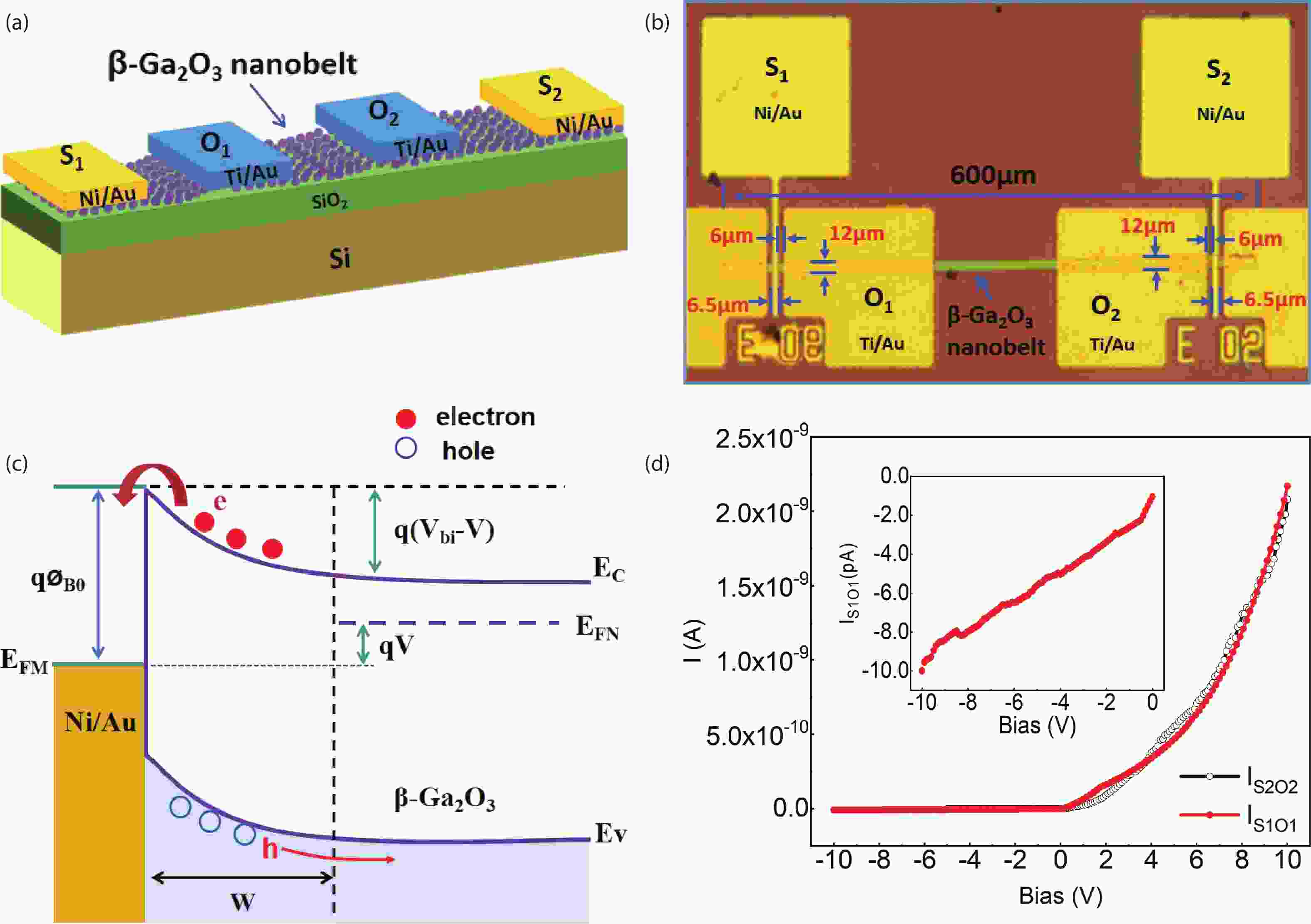
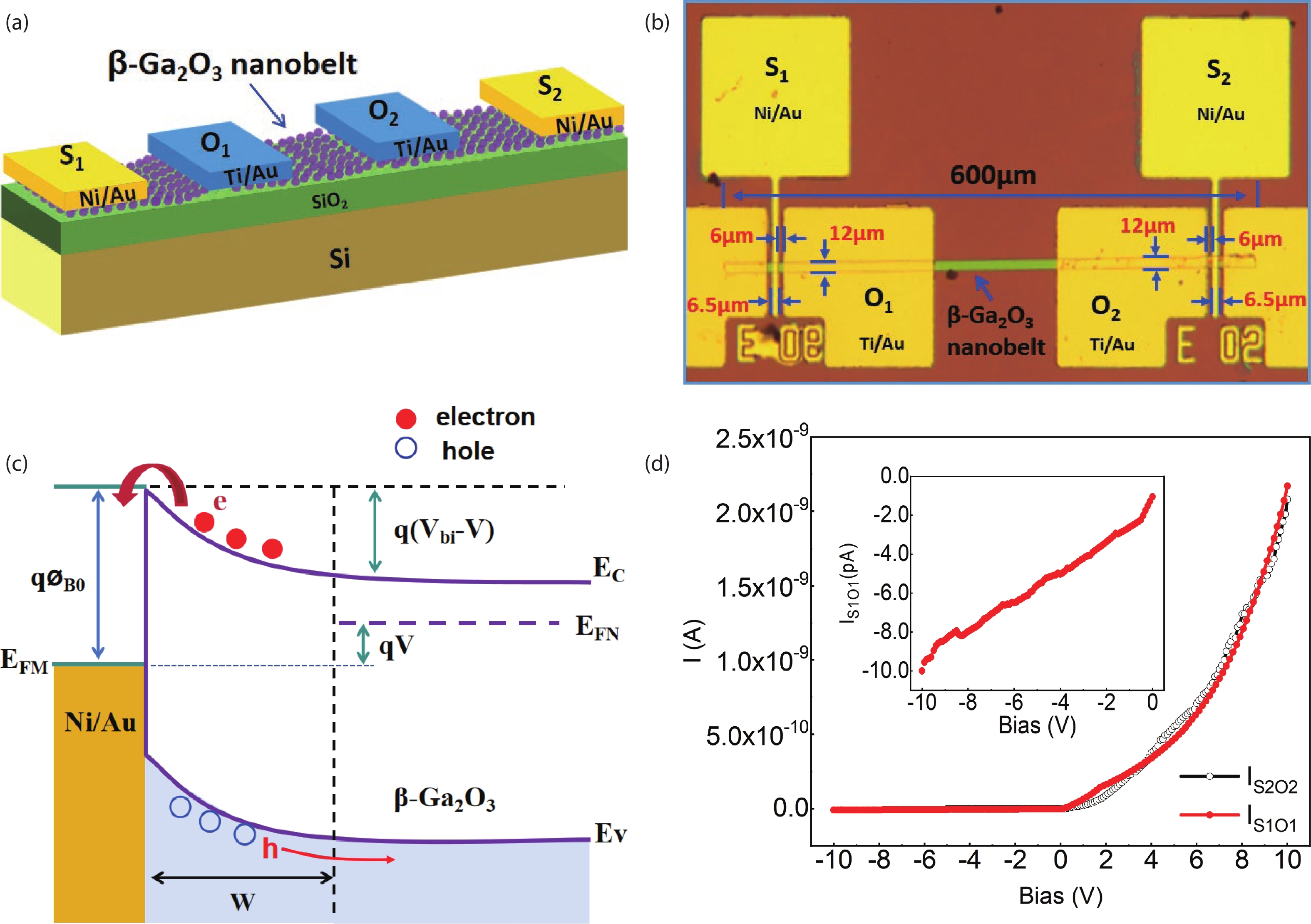
Fig. 2.  (Color online) (a) Schematic diagram of device structure. (b) Image of the actual fabricated device. (c) Energy band of Schottky-junction under positive bias. W is the width of depletion layer. (d) IV curves of Schottky-junctions of S1−O1 and S2−O2, respectively.

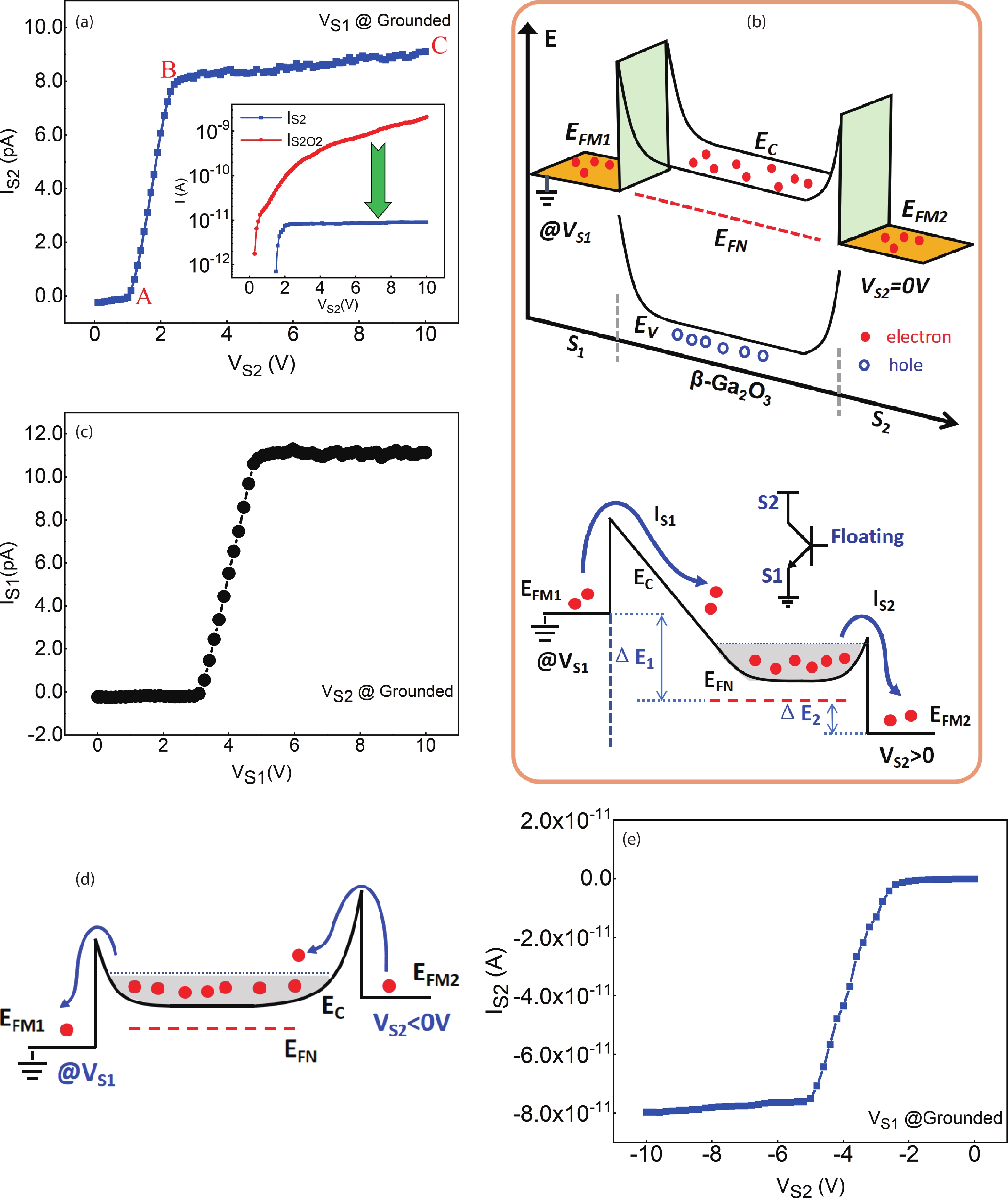
Fig. 3.  (Color online) (a) Experimental IS2VS2 curve of DSCD in the case of VS > 0 V. (b) Schematic diagram of energy band of device with grounded S1. The upper part is the case of VS = 0 V. The bottom part is the case of VS > 0 V. (c) Experimental IS1VS1 curve when S2 is grounded. (d) Band diagram when VS2 is negative. (e) Experimental IS2VS2 curve in the case of VS2 < 0 V.

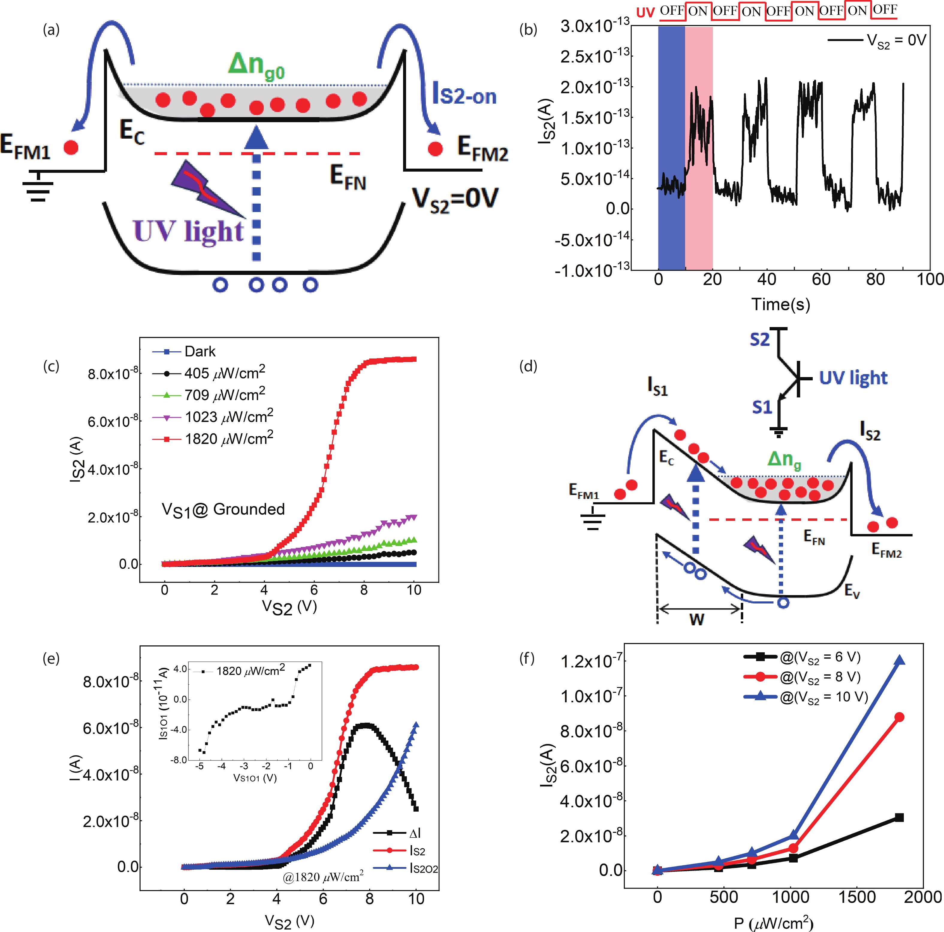
Fig. 4.  (Color online) (a) Schematic diagram of energy bands and current generated by photogenerated electrons at VS2 = 0 V. (b) Experimental IT curve under UV switching conditions at VS2 = 0 V, (c) IV curves of different power densities of 254 nm solar-blind UV light irradiation. (d) Energy band diagram of the device under UV light at VS > 0 V. (e) Comparison of IS2O2, IS1O1 and IS2 under UV illumination. (f) The relationship of P and IS2 under different VS2.

Fig. 5.  (Color online) Photoelectric parametes at VS2 = 10 V under different P. (a) PDCR and R. (b) EQE and D*.

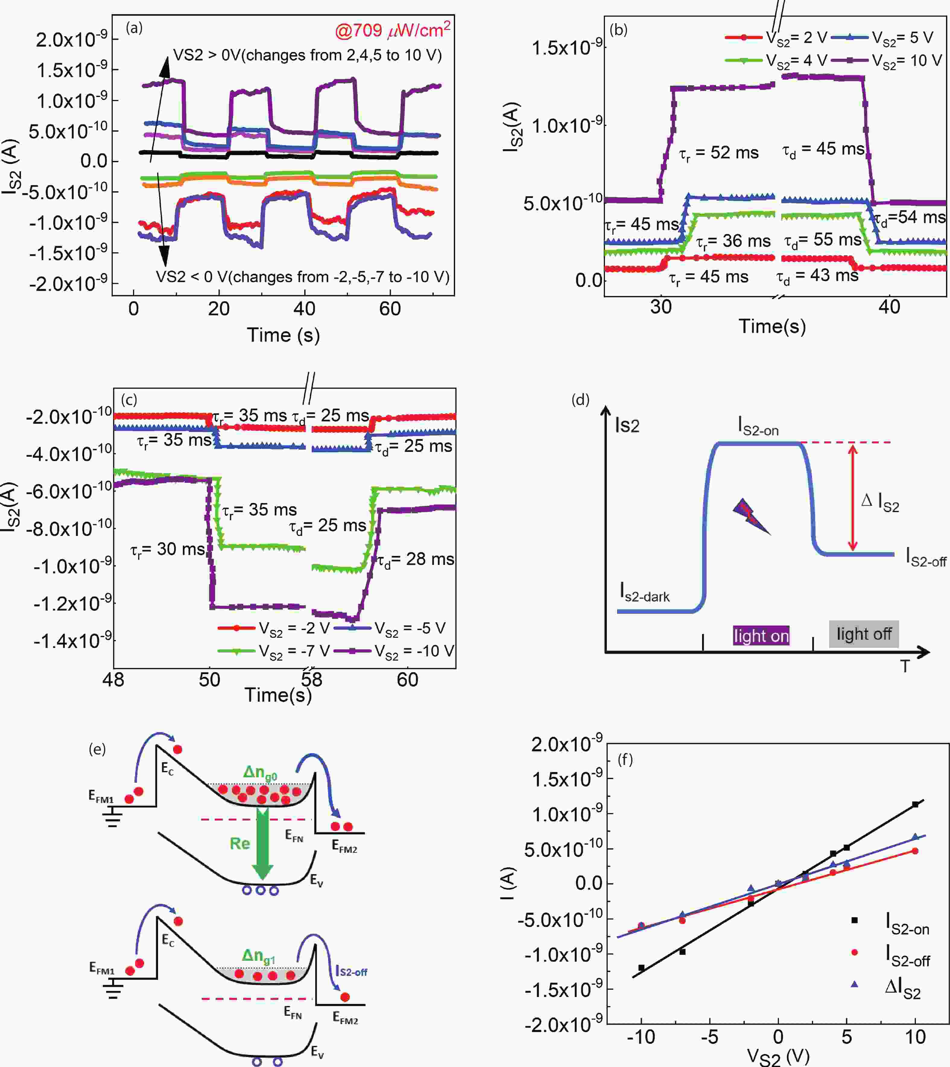
Fig. 6.  (Color online) (a) Experimental IT curves with different VS2 under 709 μW/cm2 UV irradiation. (b) and (c) Rise and decay time curves under conditons of VS2 > 0 V and VS2 < 0 V, respectively. (d) Schematic diagram of current of UV light turn-on and turn-off cases. (e) Schematic diagram of recombination process of generated-electrons during turn-off time. (f) Relationships between IS2 and VS2 during UV light turn-on and turn-off conditions.

[1]
Stepanov S I, Nikolaev V I, Bougrov V E, et al. Gallium oxide: Properties and applications-A review. Rev Adv Mater Sci, 2016, 44, 63
[2]
Higashiwaki M, Murakami H, Kumagai Y, et al. Current status of Ga2O3 power devices. Jpn J Appl Phys, 2016, 55, 1202A1 doi: 10.7567/JJAP.55.1202A1
[3]
Higashiwaki M, Sasaki K, Murakami H, et al. Recent progress in Ga2O3 power devices. Semicond Sci Technol, 2016, 31, 034001 doi: 10.1088/0268-1242/31/3/034001
[4]
Yadav M K, Mondal A, Sharma S K, et al. Substrate orientation dependent current transport mechanisms in β-Ga2O3/Si based Schottky barrier diodes. J Vac Sci Technol A Vac Surf Films, 2021, 39, 033203 doi: 10.1116/6.0000858
[5]
Wang Y B, Xu W H, You T G, et al. β-Ga2O3 MOSFETs on the Si substrate fabricated by the ion-cutting process. Sci China Phys Mech Astron, 2020, 63, 277311 doi: 10.1007/s11433-020-1533-0
[6]
Zhou H, Si M W, Alghamdi S, et al. High-performance depletion/enhancement-ode β-Ga2O3 on insulator (GOOI) field-effect transistors with record drain currents of 600/450 mA/mm. IEEE Electron Device Lett, 2017, 38, 103 doi: 10.1109/LED.2016.2635579
[7]
Yadav M K, Mondal A, Shringi S, et al. Performance enhancement of β-Ga2O3 on Si(100) based Schottky barrier diodes using reduced surface field. Semicond Sci Technol, 2020, 35, 085009 doi: 10.1088/1361-6641/ab8e64
[8]
Abdullah Q N, Ahmed A R, Ali A M, et al. Novel SnO2-coated β-Ga2O3 nanostructures for room temperature hydrogen gas sensor. Int J Hydrog Energy, 2021, 46, 7000 doi: 10.1016/j.ijhydene.2020.11.109
[9]
Liu Z, Li P G, Zhi Y S, et al. Review of gallium oxide based field-effect transistors and Schottky barrier diodes. Chin Phys B, 2019, 28, 017105 doi: 10.1088/1674-1056/28/1/017105
[10]
Guo D Y, Chen K, Wang S L, et al. Self-powered solar-blind photodetectors based on α/β phase junction of Ga2O3. Phys Rev Appl, 2020, 13, 024051 doi: 10.1103/PhysRevApplied.13.024051
[11]
Qin Y, Li L H, Zhao X L, et al. Metal–semiconductor–metal ε-Ga2O3 solar-blind photodetectors with a record-high responsivity rejection ratio and their gain mechanism. ACS Photonics, 2020, 7, 812 doi: 10.1021/acsphotonics.9b01727
[12]
Xiang X Q, Li L H, Chen C, et al. Unintentional doping effect in Si-doped MOCVD β-Ga2O3 films: Shallow donor states. Sci China Mater, 2023, 66, 748 doi: 10.1007/s40843-022-2167-x
[13]
Li L, Auer E, Liao M Y, et al. Deep-ultraviolet solar-blind photoconductivity of individual gallium oxide nanobelts. Nanoscale, 2011, 3, 1120 doi: 10.1039/c0nr00702a
[14]
Zhao B, Wang F, Chen H Y, et al. An ultrahigh responsivity (9.7 mA W–1) self-powered solar-blind photodetector based on individual ZnO–Ga2O3 heterostructures. Adv Funct Materials, 2017, 27, 1700264 doi: 10.1002/adfm.201700264
[15]
Kaur D, Kumar M. A strategic review on gallium oxide based deep-ultraviolet photodetectors: Recent progress and future prospects. Adv Opt Mater, 2021, 9, 2002160 doi: 10.1002/adom.202002160
[16]
Weng W Y, Hsueh T J, Chang S J, et al. A solar-blind β-Ga2O3 nanowire photodetector. IEEE Photonics Technol Lett, 2010, 22, 709 doi: 10.1109/LPT.2010.2044570
[17]
Wu Y L, Chang S J, Weng W Y, et al. Ga2O3 nanowire photodetector prepared on SiO2/Si template. IEEE Sens J, 2013, 13, 2368 doi: 10.1109/JSEN.2013.2247996
[18]
Oh S, Kim J, Ren F, et al. Quasi-two-dimensional β-gallium oxide solar-blind photodetectors with ultrahigh responsivity. J Mater Chem C, 2016, 4, 9245 doi: 10.1039/C6TC02467J
[19]
Suzuki R, Nakagomi S, Kokubun Y, et al. Enhancement of responsivity in solar-blind β-Ga2O3 photodiodes with a Au Schottky contact fabricated on single crystal substrates by annealing. Appl Phys Lett, 2009, 94, 222102 doi: 10.1063/1.3147197
[20]
Chen X, Liu K W, Zhang Z Z, et al. Self-powered solar-blind photodetector with fast response based on Au/β-Ga2O3 nanowires array film Schottky-junction. ACS Appl Mater Interfaces, 2016, 8, 4185 doi: 10.1021/acsami.5b11956
[21]
Kim S, Kim J. Highly selective ozone-treated β-Ga2O3 solar-blind deep-UV photodetectors. Appl Phys Lett, 2020, 117, 261101 doi: 10.1063/5.0030400
[22]
Zhang Y B, Zheng J, Ma P P, et al. Growth and characterization of β-Ga2O3 thin films grown on off-angled Al2O3 substrates by metal-organic chemical vapor deposition. J Semicond, 2022, 43, 092801 doi: 10.1088/1674-4926/43/9/092801
[23]
Qi Q, Chen H F, Hong Z F, et al. Preparation and characteristics of ultra-wide Ga2O3 nanoribbons up to millimeter-long level without catalyst. Acta Phys Sin, 2020, 69, 168101 doi: 10.7498/aps.69.20200481
[24]
Shih H Y, Chu F C, Das A, et al. Atomic layer deposition of gallium oxide films as gate dielectrics in AlGaN/GaN metal-oxide-semiconductor high-electron-mobility transistors. Nanoscale Res Lett, 2016, 11, 235 doi: 10.1186/s11671-016-1448-z
[25]
Wu C, Wu F M, Hu H Z, et al. Review of self-powered solar-blind photodetectors based on Ga2O3. Mater Today Phys, 2022, 28, 100883 doi: 10.1016/j.mtphys.2022.100883
[26]
Kumar A, Bag A. High responsivity of quasi-2D electrospun β-Ga2O3-based deep-UV photodetectors. IEEE Photonics Technol Lett, 2019, 31, 619 doi: 10.1109/LPT.2019.2901236
[27]
He H L, Wu C, Hu H Z, et al. Bandgap engineering and oxygen vacancy defect electroactivity inhibition in highly crystalline N-alloyed Ga2O3 films through plasma-enhanced technology. J Phys Chem Lett, 2023, 14, 6444 doi: 10.1021/acs.jpclett.3c01368
[28]
Cheng Y X, Ye J H, Lai L, et al. Ambipolarity regulation of deep-UV photocurrent by controlling crystalline phases in Ga2O3 nanostructure for switchable logic applications. Adv Elect Materials, 2023, 9, 2201216 doi: 10.1002/aelm.202201216
[29]
Wang Z P, Gong H H, Yu X X, et al. Trap-mediated bipolar charge transport in NiO/Ga2O3 p+-n heterojunction power diodes. Sci China Mater, 2022, 66, 1157 doi: 10.1007/s40843-022-2244-y
[30]
Li Y Q, Zhang D, Jia L M, et al. Ultrawide-bandgap (6.14 eV) (AlGa)2O3/Ga2O3 heterostructure designed by lattice matching strategy for highly sensitive vacuum ultraviolet photodetection. Sci China Mater, 2021, 64, 3027 doi: 10.1007/s40843-021-1698-3
[31]
Chen R R, Wang D, Feng B, et al. High responsivity self-powered DUV photodetectors based on β-Ga2O3/GaN heterogeneous PN junctions. Vacuum, 2023, 215, 112332 doi: 10.1016/j.vacuum.2023.112332
[32]
Bielecki Z, Achtenberg K, Kopytko M, et al. Review of photodetectors characterization methods. Bull Pol Acad Sci Tech Sci, 2022, 70, 144608 doi: 10.24425/bpasts.2022.140534
[33]
Wang D, Ma X C, Chen R R, et al. Solar-blind ultraviolet photodetectors based on Ta-doped β-Ga2O3 heteroepitaxial films. Opt Mater, 2022, 129, 112491 doi: 10.1016/j.optmat.2022.112491
[34]
Vasudevan A, Jung S, Ji T, et al. Quasi-symmetric Wheatstone bridge zinc oxide nanorod UV detectors. IEEE Sens J, 2014, 14, 3310 doi: 10.1109/JSEN.2014.2328871
[35]
Liu N S, Fang G J, Zeng W, et al. Direct growth of lateral ZnO nanorod UV photodetectors with Schottky contact by a single-step hydrothermal reaction. ACS Appl Mater Interfaces, 2010, 2, 1973 doi: 10.1021/am100277q
[36]
Sheoran H, Fang S, Liang F Z, et al. High performance of zero-power-consumption MOCVD-grown β-Ga2O3-based solar-blind photodetectors with ultralow dark current and high-temperature functionalities. ACS Appl Mater Interfaces, 2022, 14, 52096 doi: 10.1021/acsami.2c08511
  • Search

    Advanced Search >>

    GET CITATION

    shu

    Export: BibTex EndNote

    Article Metrics

    Article views: 580 Times PDF downloads: 43 Times Cited by: 0 Times

    History

    Received: 06 December 2023 Revised: 10 January 2024 Online: Accepted Manuscript: 22 January 2024Uncorrected proof: 31 January 2024Published: 10 May 2024

    Catalog

      Email This Article

      User name:
      Email:*请输入正确邮箱
      Code:*验证码错误
      Haifeng Chen, Xiaocong Han, Chenlu Wu, Zhanhang Liu, Shaoqing Wang, Xiangtai Liu, Qin Lu, Yifan Jia, Zhan Wang, Yunhe Guan, Lijun Li, Yue Hao. Dual-Schottky-junctions coupling device based on ultra-long β-Ga2O3 single-crystal nanobelt and its photoelectric properties[J]. Journal of Semiconductors, 2024, 45(5): 052502. doi: 10.1088/1674-4926/45/5/052502 H F Chen, X C Han, C L Wu, Z H Liu, S Q Wang, X T Liu, Q Lu, Y F Jia, Z Wang, Y H Guan, L J Li, and Y Hao, Dual-Schottky-junctions coupling device based on ultra-long β-Ga2O3 single-crystal nanobelt and its photoelectric properties[J]. J. Semicond., 2024, 45(5), 052502 doi: 10.1088/1674-4926/45/5/052502Export: BibTex EndNote
      Citation:
      Haifeng Chen, Xiaocong Han, Chenlu Wu, Zhanhang Liu, Shaoqing Wang, Xiangtai Liu, Qin Lu, Yifan Jia, Zhan Wang, Yunhe Guan, Lijun Li, Yue Hao. Dual-Schottky-junctions coupling device based on ultra-long β-Ga2O3 single-crystal nanobelt and its photoelectric properties[J]. Journal of Semiconductors, 2024, 45(5): 052502. doi: 10.1088/1674-4926/45/5/052502

      H F Chen, X C Han, C L Wu, Z H Liu, S Q Wang, X T Liu, Q Lu, Y F Jia, Z Wang, Y H Guan, L J Li, and Y Hao, Dual-Schottky-junctions coupling device based on ultra-long β-Ga2O3 single-crystal nanobelt and its photoelectric properties[J]. J. Semicond., 2024, 45(5), 052502 doi: 10.1088/1674-4926/45/5/052502
      Export: BibTex EndNote

      Dual-Schottky-junctions coupling device based on ultra-long β-Ga2O3 single-crystal nanobelt and its photoelectric properties

      doi: 10.1088/1674-4926/45/5/052502
      More Information
      • Author Bio:

        Haifeng Chen Haifeng Chen received the Ph. D. degree from Xidian University in 2008. He is currently a Professor at the Xi’an University of Posts and Telecommunications. His research interests focus on Ga2O3 material and devices

      • Corresponding author: chenhaifeng@xupt.edu.cn
      • Received Date: 2023-12-06
      • Revised Date: 2024-01-10
      • Available Online: 2024-01-22

      Catalog

        /

        DownLoad:  Full-Size Img  PowerPoint
        Return
        Return