


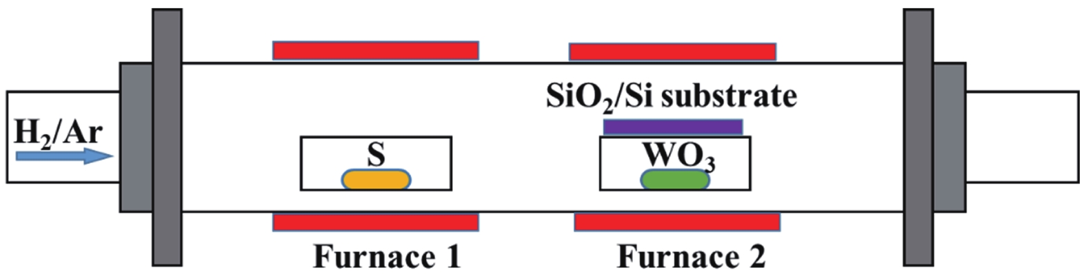
Fig. 1.
(Color online) Experimental setup of the CVD growth of monolayer WS2 sample.
ARTICLES
Yao Li1, Haiou Zhu1, 2 and Zongpeng Song2,
Corresponding author: Zongpeng Song, songzongpeng@sztu.edu.cn
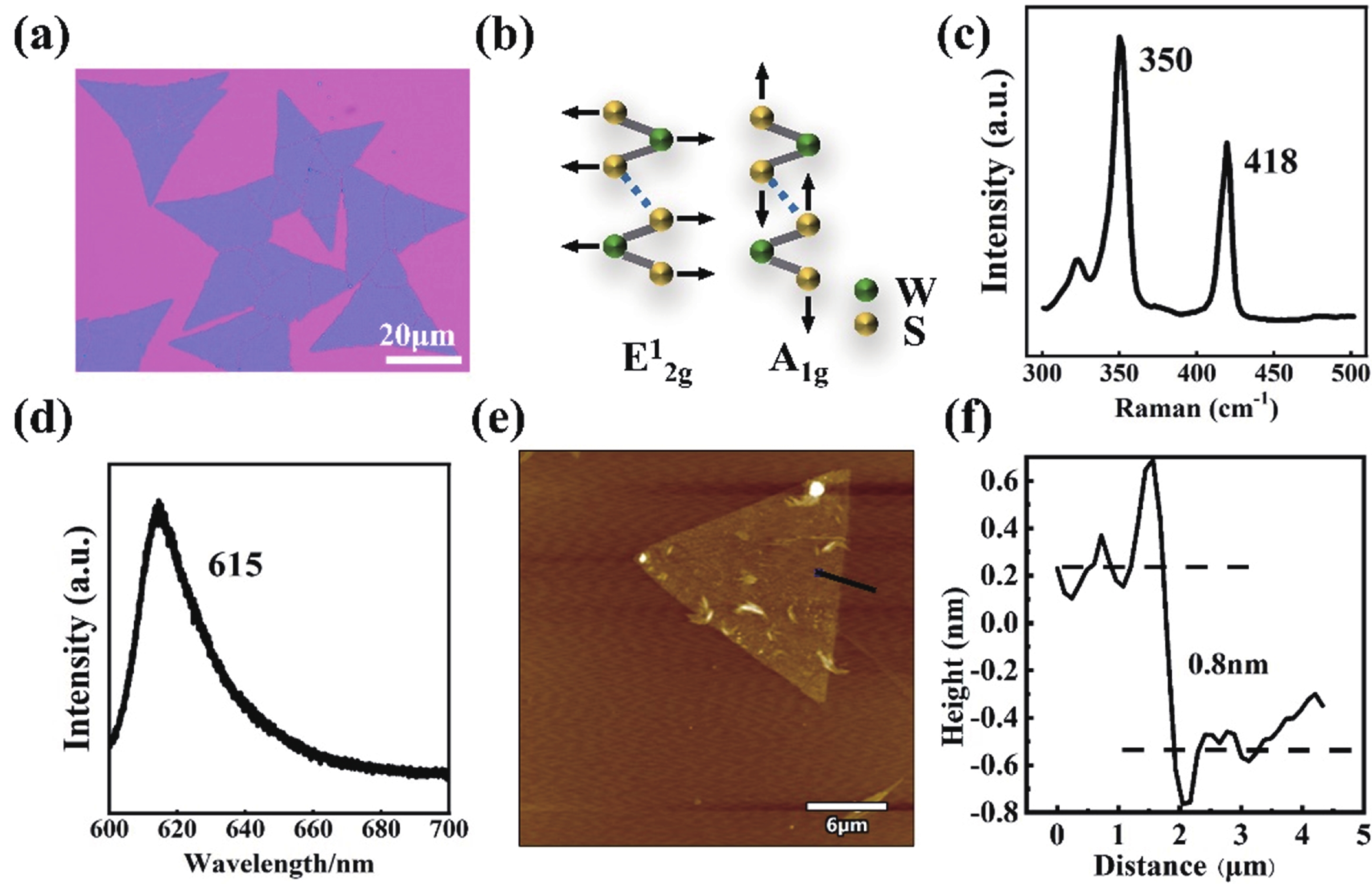
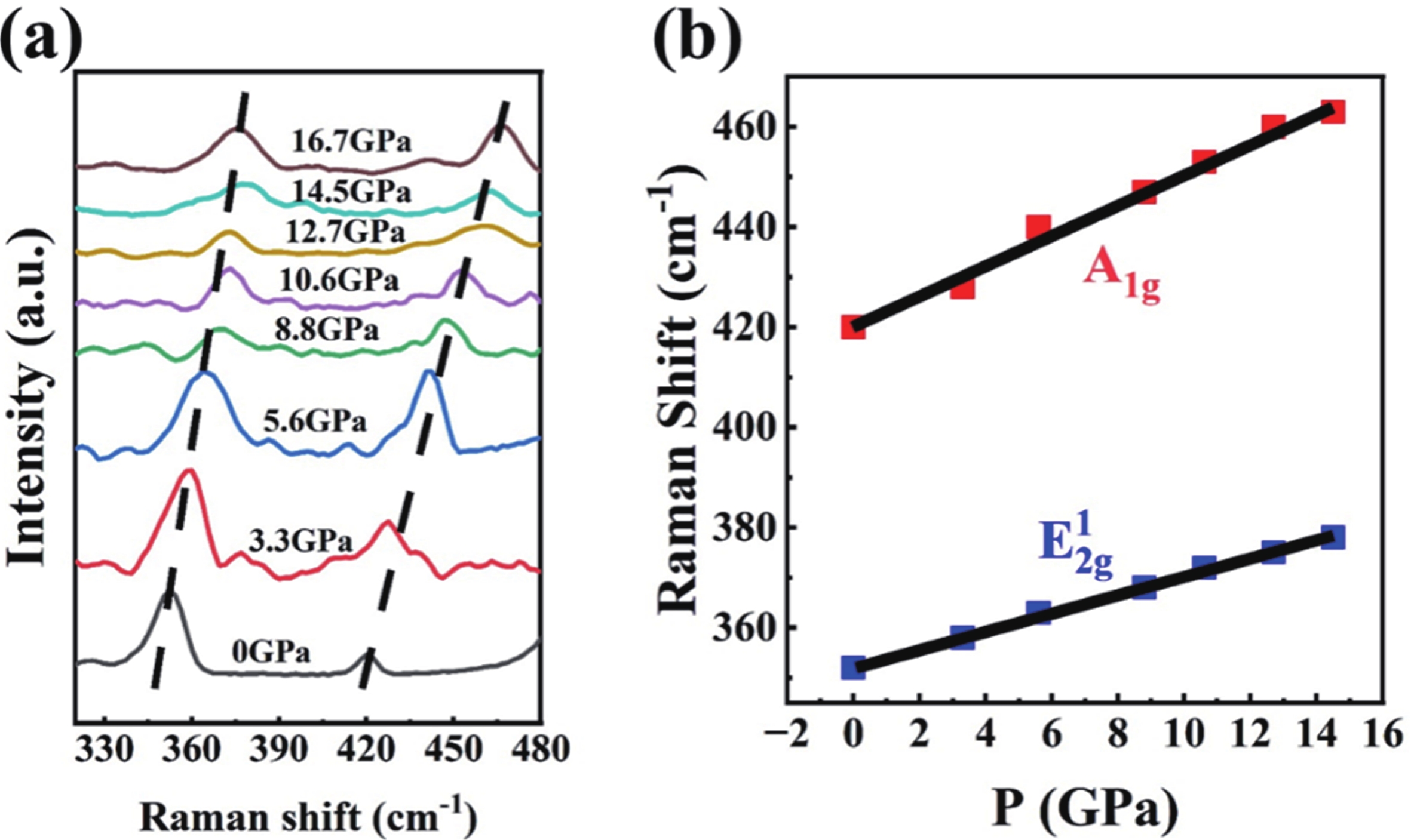
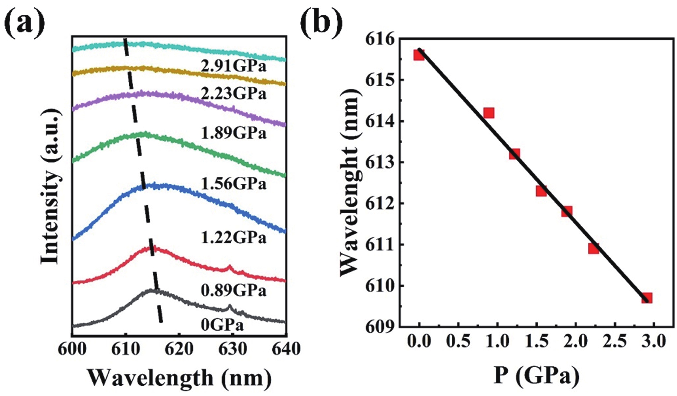
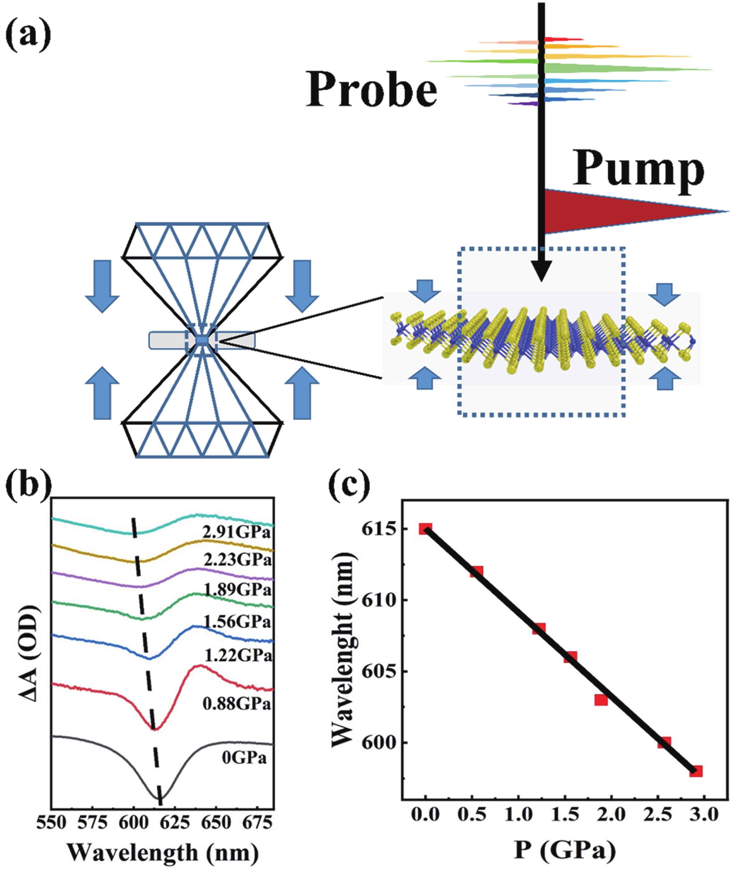
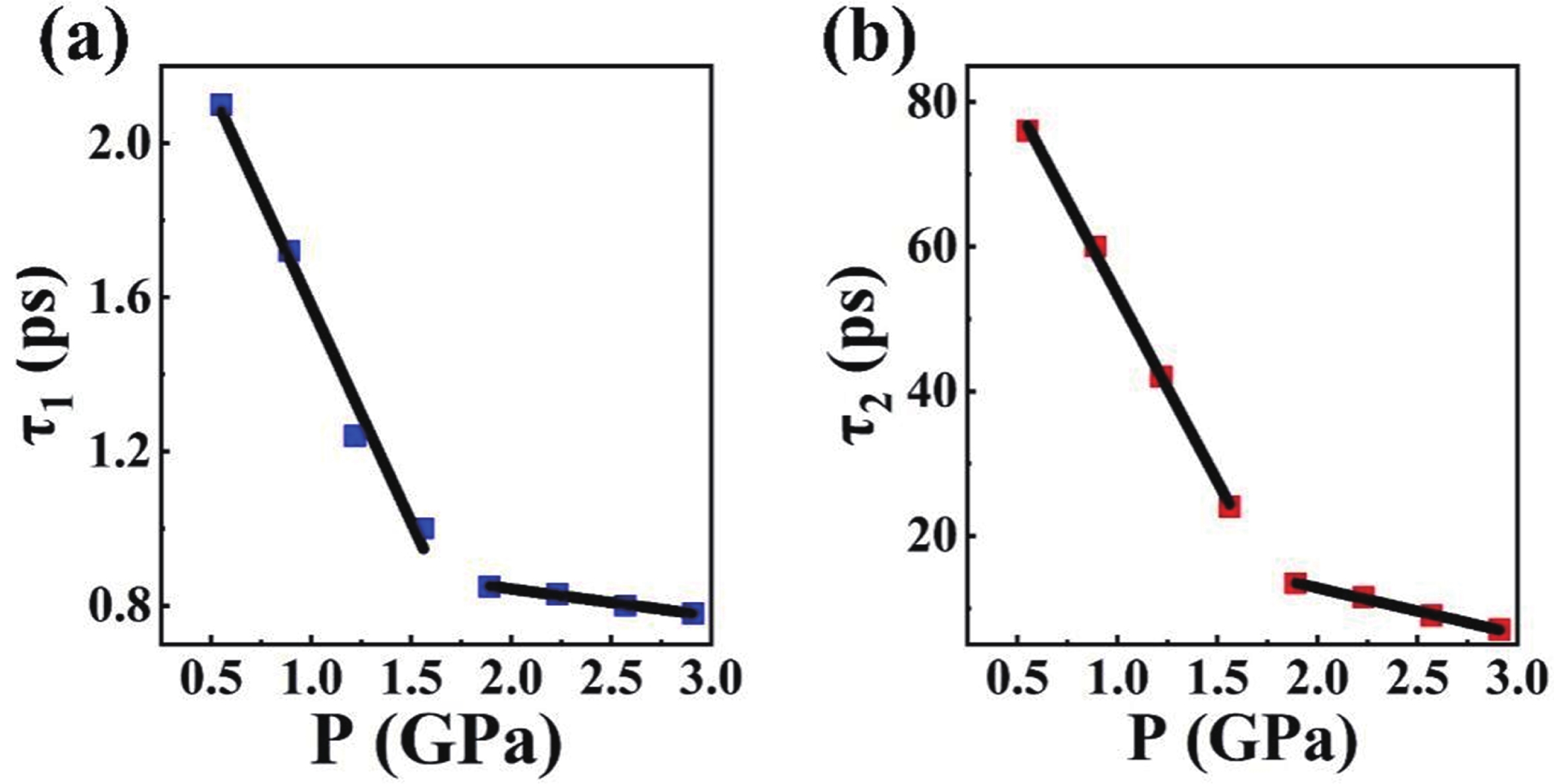
Abstract: Two-dimensional transition metal dichalcogenides (TMDs) have intriguing physic properties and offer an exciting platform to explore many features that are important for future devices. In this work, we synthesized monolayer WS2 as an example to study the optical response with hydrostatic pressure. The Raman results show a continuous tuning of the lattice vibrations that is induced by hydrostatic pressure. We further demonstrate an efficient pressure-induced change of the band structure and carrier dynamics via transient absorption measurements. We found that two time constants can be attributed to the capture process of two kinds of defect states, with the pressure increasing from 0.55 GPa to 2.91 GPa, both of capture processes were accelerated, and there is an inflection point within the pressure range of 1.56 GPa to 1.89 GPa. Our findings provide valuable information for the design of future optoelectronic devices.
Key words: two-dimensional transition metal dichalcogenides, hydrostatic pressure, carrier dynamics, band structure, ultrafast spectroscopy
| [1] |
Sharma I, Mehta B R. Enhanced charge separation at 2D MoS2/ZnS heterojunction: KPFM based study of interface photovoltage. Appl Phys Lett, 2017, 110, 061602 doi: 10.1063/1.4975779
|
| [2] |
Ross R T, Nozik A J. Efficiency of hot-carrier solar energy converters. J Appl Phys, 1982, 53, 3813 doi: 10.1063/1.331124
|
| [3] |
Liu H S, Han N N, Zhao J J. Atomistic insight into the oxidation of monolayer transition metal dichalcogenides: From structures to electronic properties. RSC Adv, 2015, 5, 17572 doi: 10.1039/C4RA17320A
|
| [4] |
Parzinger E, Miller B, Blaschke B, et al. Photocatalytic stability of single- and few-layer MoS2. ACS Nano, 2015, 9, 11302 doi: 10.1021/acsnano.5b04979
|
| [5] |
Wang Q H, Kalantar-Zadeh K, Kis A, et al. Electronics and optoelectronics of two-dimensional transition metal dichalcogenides. Nat Nanotechnol, 2012, 7, 699 doi: 10.1038/nnano.2012.193
|
| [6] |
Geim A K, Grigorieva I V. Van der Waals heterostructures. Nature, 2013, 499, 419 doi: 10.1038/nature12385
|
| [7] |
Yin Z Y, Li H, Li H, et al. Single-layer MoS2 phototransistors. ACS Nano, 2012, 6, 74 doi: 10.1021/nn2024557
|
| [8] |
Choi W, Cho M Y, Konar A, et al. High-detectivity multilayer MoS2 phototransistors with spectral response from ultraviolet to infrared. Adv Mater, 2012, 24, 5832 doi: 10.1002/adma.201201909
|
| [9] |
He Y M, Yang Y, Zhang Z H, et al. Strain-induced electronic structure changes in stacked van der Waals heterostructures. Nano Lett, 2016, 16, 3314 doi: 10.1021/acs.nanolett.6b00932
|
| [10] |
Chen M, Xia J A, Zhou J D, et al. Ordered and atomically perfect fragmentation of layered transition metal dichalcogenides via mechanical instabilities. ACS Nano, 2017, 11, 9191 doi: 10.1021/acsnano.7b04158
|
| [11] |
Nayak A P, Yuan Z, Cao B X, et al. Pressure-modulated conductivity, carrier density, and mobility of multilayered tungsten disulfide. ACS Nano, 2015, 9, 9117 doi: 10.1021/acsnano.5b03295
|
| [12] |
Zhu Z Y, Cheng Y C, Schwingenschlögl U. Giant spin-orbit-induced spin splitting in two-dimensional transition-metal dichalcogenide semiconductors. Phys Rev B, 2011, 84, 153402 doi: 10.1103/PhysRevB.84.153402
|
| [13] |
Ye Z L, Cao T, O’Brien K, et al. Probing excitonic dark states in single-layer tungsten disulphide. Nature, 2014, 513, 214 doi: 10.1038/nature13734
|
| [14] |
Selvi E, Ma Y Z, Aksoy R, et al. High pressure X-ray diffraction study of tungsten disulfide. J Phys Chem Solids, 2006, 67, 2183 doi: 10.1016/j.jpcs.2006.05.008
|
| [15] |
Hangyo M, Nakashima S I, Mitsuishi A. Raman spectroscopic studies of MX2-type layered compounds. Ferroelectrics, 1983, 52, 151 doi: 10.1080/00150198308208248
|
| [16] |
Ramakrishna Matte H S S, Gomathi A, Manna A, et al. MoS2 and WS2 analogues of graphene. Angew Chem Int Ed, 2010, 49, 4059 doi: 10.1002/anie.201000009
|
| [17] |
Duwal S, Yoo C S. Shear-induced isostructural phase transition and metallization of layered tungsten disulfide under nonhydrostatic compression. J Phys Chem C, 2016, 120, 5101 doi: 10.1021/acs.jpcc.5b10759
|
| [18] |
Livneh T, Sterer E. Resonant Raman scattering at exciton states tuned by pressure and temperature in 2H-MoS2. Phys Rev B, 2010, 81, 195209 doi: 10.1103/PhysRevB.81.195209
|
| [19] |
Nicolle J, Machon D, Poncharal P, et al. Pressure-mediated doping in graphene. Nano Lett, 2011, 11, 3564 doi: 10.1021/nl201243c
|
| [20] |
Cheng X R, Li Y Y, Shang J M, et al. Thickness-dependent phase transition and optical behavior of MoS2 films under high pressure. Nano Res, 2018, 11, 855 doi: 10.1007/s12274-017-1696-y
|
| [21] |
Chi Z H, Zhao X M, Zhang H D, et al. Pressure-induced metallization of molybdenum disulfide. Phys Rev Lett, 2014, 113, 036802 doi: 10.1103/PhysRevLett.113.036802
|
| [22] |
Nayak A P, Pandey T, Voiry D, et al. Pressure-dependent optical and vibrational properties of monolayer molybdenum disulfide. Nano Lett, 2015, 15, 346 doi: 10.1021/nl5036397
|
| [23] |
Dou X M, Ding K, Jiang D S, et al. Tuning and identification of interband transitions in monolayer and bilayer molybdenum disulfide using hydrostatic pressure. ACS Nano, 2014, 8, 7458 doi: 10.1021/nn502717d
|
| [24] |
Li F F, Yan Y L, Han B, et al. Pressure confinement effect in MoS2 monolayers. Nanoscale, 2015, 7, 9075 doi: 10.1039/C5NR00580A
|
| [25] |
Xia J, Yan J X, Wang Z H, et al. Strong coupling and pressure engineering in WSe2–MoSe2 heterobilayers. Nat Phys, 2020, 17, 92 doi: 10.1038/s41567-020-1005-7
|
| [26] |
Wang H N, Zhang C J, Rana F. Ultrafast dynamics of defect-assisted electron–hole recombination in monolayer MoS2. Nano Lett, 2015, 15, 339 doi: 10.1021/nl503636c
|
| [27] |
Cunningham P D, McCreary K M, Hanbicki A T, et al. Charge trapping and exciton dynamics in large-area CVD grown MoS2. J Phys Chem C, 2016, 120, 5819 doi: 10.1021/acs.jpcc.6b00647
|
| [28] |
Wang M S, Li W, Scarabelli L, et al. Plasmon-trion and plasmon-exciton resonance energy transfer from a single plasmonic nanoparticle to monolayer MoS2. Nanoscale, 2017, 9, 13947 doi: 10.1039/C7NR03909C
|
| [29] |
Ruppert C, Chernikov A, Hill H M, et al. The role of electronic and phononic excitation in the optical response of monolayer WS2 after ultrafast excitation. Nano Lett, 2017, 17, 644 doi: 10.1021/acs.nanolett.6b03513
|
| [30] |
Li Y Z, Shi J A, Mi Y, et al. Ultrafast carrier dynamics in two-dimensional transition metal dichalcogenides. J Mater Chem C, 2019, 7, 4304 doi: 10.1039/C8TC06343E
|
| [31] |
Ahn C, Lim H. Synthesis of monolayer 2D MoS2 quantum dots and nanomesh films by inorganic molecular chemical vapor deposition for quantum confinement effect control. Bull Korean Chem Soc, 2022, 43, 1184 doi: 10.1002/bkcs.12608
|
| [32] |
Sridevi R, Pravin J C, Babu A R, et al. Investigation of quantum confinement effects on molybdenum disulfide (MoS2) based transistor using ritz Galerkin finite element technique. Silicon, 2022, 14, 2157 doi: 10.1007/s12633-021-01010-w
|
| [33] |
Trovatello C, Katsch F, Li Q Y, et al. Disentangling many-body effects in the coherent optical response of 2D semiconductors. Nano Lett, 2022, 22, 5322 doi: 10.1021/acs.nanolett.2c01309
|


Article views: 924 Times PDF downloads: 63 Times Cited by: 0 Times
Received: 27 February 2023 Revised: 27 March 2023 Online: Accepted Manuscript: 25 May 2023Uncorrected proof: 28 June 2023Corrected proof: 14 July 2023Published: 10 August 2023
| Citation: |
Yao Li, Haiou Zhu, Zongpeng Song. Pressure manipulation of ultrafast carrier dynamics in monolayer WS2[J]. Journal of Semiconductors, 2023, 44(8): 082001. doi: 10.1088/1674-4926/44/8/082001
****
Y Li, H O Zhu, Z P Song. Pressure manipulation of ultrafast carrier dynamics in monolayer WS2[J]. J. Semicond, 2023, 44(8): 082001. doi: 10.1088/1674-4926/44/8/082001

|
 Yao Li:is an M.S. student at the Shenzhen Technology University under the supervision of Prof. Haiou Zhu. His research focuses on the dynamic behavior of high-pressure carriers based on TMDs
 Zongpeng Song is an optical testing engineer in the analysis and testing center of Shenzhen Technology University. He received his Ph.D. degree in optical engineering from Shenzhen University. His research focuses on ultrafast spectroscopy
| [1] |
Sharma I, Mehta B R. Enhanced charge separation at 2D MoS2/ZnS heterojunction: KPFM based study of interface photovoltage. Appl Phys Lett, 2017, 110, 061602 doi: 10.1063/1.4975779
|
| [2] |
Ross R T, Nozik A J. Efficiency of hot-carrier solar energy converters. J Appl Phys, 1982, 53, 3813 doi: 10.1063/1.331124
|
| [3] |
Liu H S, Han N N, Zhao J J. Atomistic insight into the oxidation of monolayer transition metal dichalcogenides: From structures to electronic properties. RSC Adv, 2015, 5, 17572 doi: 10.1039/C4RA17320A
|
| [4] |
Parzinger E, Miller B, Blaschke B, et al. Photocatalytic stability of single- and few-layer MoS2. ACS Nano, 2015, 9, 11302 doi: 10.1021/acsnano.5b04979
|
| [5] |
Wang Q H, Kalantar-Zadeh K, Kis A, et al. Electronics and optoelectronics of two-dimensional transition metal dichalcogenides. Nat Nanotechnol, 2012, 7, 699 doi: 10.1038/nnano.2012.193
|
| [6] |
Geim A K, Grigorieva I V. Van der Waals heterostructures. Nature, 2013, 499, 419 doi: 10.1038/nature12385
|
| [7] |
Yin Z Y, Li H, Li H, et al. Single-layer MoS2 phototransistors. ACS Nano, 2012, 6, 74 doi: 10.1021/nn2024557
|
| [8] |
Choi W, Cho M Y, Konar A, et al. High-detectivity multilayer MoS2 phototransistors with spectral response from ultraviolet to infrared. Adv Mater, 2012, 24, 5832 doi: 10.1002/adma.201201909
|
| [9] |
He Y M, Yang Y, Zhang Z H, et al. Strain-induced electronic structure changes in stacked van der Waals heterostructures. Nano Lett, 2016, 16, 3314 doi: 10.1021/acs.nanolett.6b00932
|
| [10] |
Chen M, Xia J A, Zhou J D, et al. Ordered and atomically perfect fragmentation of layered transition metal dichalcogenides via mechanical instabilities. ACS Nano, 2017, 11, 9191 doi: 10.1021/acsnano.7b04158
|
| [11] |
Nayak A P, Yuan Z, Cao B X, et al. Pressure-modulated conductivity, carrier density, and mobility of multilayered tungsten disulfide. ACS Nano, 2015, 9, 9117 doi: 10.1021/acsnano.5b03295
|
| [12] |
Zhu Z Y, Cheng Y C, Schwingenschlögl U. Giant spin-orbit-induced spin splitting in two-dimensional transition-metal dichalcogenide semiconductors. Phys Rev B, 2011, 84, 153402 doi: 10.1103/PhysRevB.84.153402
|
| [13] |
Ye Z L, Cao T, O’Brien K, et al. Probing excitonic dark states in single-layer tungsten disulphide. Nature, 2014, 513, 214 doi: 10.1038/nature13734
|
| [14] |
Selvi E, Ma Y Z, Aksoy R, et al. High pressure X-ray diffraction study of tungsten disulfide. J Phys Chem Solids, 2006, 67, 2183 doi: 10.1016/j.jpcs.2006.05.008
|
| [15] |
Hangyo M, Nakashima S I, Mitsuishi A. Raman spectroscopic studies of MX2-type layered compounds. Ferroelectrics, 1983, 52, 151 doi: 10.1080/00150198308208248
|
| [16] |
Ramakrishna Matte H S S, Gomathi A, Manna A, et al. MoS2 and WS2 analogues of graphene. Angew Chem Int Ed, 2010, 49, 4059 doi: 10.1002/anie.201000009
|
| [17] |
Duwal S, Yoo C S. Shear-induced isostructural phase transition and metallization of layered tungsten disulfide under nonhydrostatic compression. J Phys Chem C, 2016, 120, 5101 doi: 10.1021/acs.jpcc.5b10759
|
| [18] |
Livneh T, Sterer E. Resonant Raman scattering at exciton states tuned by pressure and temperature in 2H-MoS2. Phys Rev B, 2010, 81, 195209 doi: 10.1103/PhysRevB.81.195209
|
| [19] |
Nicolle J, Machon D, Poncharal P, et al. Pressure-mediated doping in graphene. Nano Lett, 2011, 11, 3564 doi: 10.1021/nl201243c
|
| [20] |
Cheng X R, Li Y Y, Shang J M, et al. Thickness-dependent phase transition and optical behavior of MoS2 films under high pressure. Nano Res, 2018, 11, 855 doi: 10.1007/s12274-017-1696-y
|
| [21] |
Chi Z H, Zhao X M, Zhang H D, et al. Pressure-induced metallization of molybdenum disulfide. Phys Rev Lett, 2014, 113, 036802 doi: 10.1103/PhysRevLett.113.036802
|
| [22] |
Nayak A P, Pandey T, Voiry D, et al. Pressure-dependent optical and vibrational properties of monolayer molybdenum disulfide. Nano Lett, 2015, 15, 346 doi: 10.1021/nl5036397
|
| [23] |
Dou X M, Ding K, Jiang D S, et al. Tuning and identification of interband transitions in monolayer and bilayer molybdenum disulfide using hydrostatic pressure. ACS Nano, 2014, 8, 7458 doi: 10.1021/nn502717d
|
| [24] |
Li F F, Yan Y L, Han B, et al. Pressure confinement effect in MoS2 monolayers. Nanoscale, 2015, 7, 9075 doi: 10.1039/C5NR00580A
|
| [25] |
Xia J, Yan J X, Wang Z H, et al. Strong coupling and pressure engineering in WSe2–MoSe2 heterobilayers. Nat Phys, 2020, 17, 92 doi: 10.1038/s41567-020-1005-7
|
| [26] |
Wang H N, Zhang C J, Rana F. Ultrafast dynamics of defect-assisted electron–hole recombination in monolayer MoS2. Nano Lett, 2015, 15, 339 doi: 10.1021/nl503636c
|
| [27] |
Cunningham P D, McCreary K M, Hanbicki A T, et al. Charge trapping and exciton dynamics in large-area CVD grown MoS2. J Phys Chem C, 2016, 120, 5819 doi: 10.1021/acs.jpcc.6b00647
|
| [28] |
Wang M S, Li W, Scarabelli L, et al. Plasmon-trion and plasmon-exciton resonance energy transfer from a single plasmonic nanoparticle to monolayer MoS2. Nanoscale, 2017, 9, 13947 doi: 10.1039/C7NR03909C
|
| [29] |
Ruppert C, Chernikov A, Hill H M, et al. The role of electronic and phononic excitation in the optical response of monolayer WS2 after ultrafast excitation. Nano Lett, 2017, 17, 644 doi: 10.1021/acs.nanolett.6b03513
|
| [30] |
Li Y Z, Shi J A, Mi Y, et al. Ultrafast carrier dynamics in two-dimensional transition metal dichalcogenides. J Mater Chem C, 2019, 7, 4304 doi: 10.1039/C8TC06343E
|
| [31] |
Ahn C, Lim H. Synthesis of monolayer 2D MoS2 quantum dots and nanomesh films by inorganic molecular chemical vapor deposition for quantum confinement effect control. Bull Korean Chem Soc, 2022, 43, 1184 doi: 10.1002/bkcs.12608
|
| [32] |
Sridevi R, Pravin J C, Babu A R, et al. Investigation of quantum confinement effects on molybdenum disulfide (MoS2) based transistor using ritz Galerkin finite element technique. Silicon, 2022, 14, 2157 doi: 10.1007/s12633-021-01010-w
|
| [33] |
Trovatello C, Katsch F, Li Q Y, et al. Disentangling many-body effects in the coherent optical response of 2D semiconductors. Nano Lett, 2022, 22, 5322 doi: 10.1021/acs.nanolett.2c01309
|

 WeChat ID
Journal of Semiconductors © 2017 All Rights Reserved 京ICP备05085259号-2

 DownLoad:

