


1. Introduction
β-gallium oxide (β-Ga2O3) is an ultra-wide bandgap (UWBG) semiconductor with superior electronic and optoelectronic properties. For one thing, due to the wide direct optical bandgap of 4.9 eV, β-Ga2O3 is widely used in deep-ultraviolet (DUV) photodetectors[1, 2]. Multifarious device configurations, including PN junction[3], PIN junction[4], heterojunction[5], Schottky photodiodes[6], MSM devices[7], avalanche photodiodes[8] and phototransistors[9, 10], have been reported based on β-Ga2O3 wafers, thin-films and nanostructures. High photoresponsivity of more than 4000 A/W[10] and response speed less than 12 ns[11] were realized. For another thing, since β-Ga2O3 features high breakdown field strength of 8 MV/cm and Baliga’s figure of merit (BFOM) of 3400, which is four times larger than GaN and 4H-SiC, it is also a promising candidate in power electronics and high-voltage devices[12]. High breakdown voltage of more than 3000 V has been reported in β-Ga2O3 Schottky diodes with lateral field-plate structure[13]. Up to 8.03 kV ultra-high breakdown voltage was achieved in field-plated lateral β-Ga2O3 MOSFETs[14]. Currently, DUV photodetector and power electronics are the two major application research interests of β-Ga2O3, while still there are some other applications, such as gas sensors[15] and X-ray detectors[16].
Given the ubiquitous applications, β-Ga2O3 has gained much attention, especially, in recent ten years. Besides, the low symmetry of crystal structure renders β-Ga2O3 exceeding anisotropic properties. In this review, we will emphasize on the unique anisotropic properties and applications of β-Ga2O3.
2. Anisotropic crystal structure of β-Ga2O3
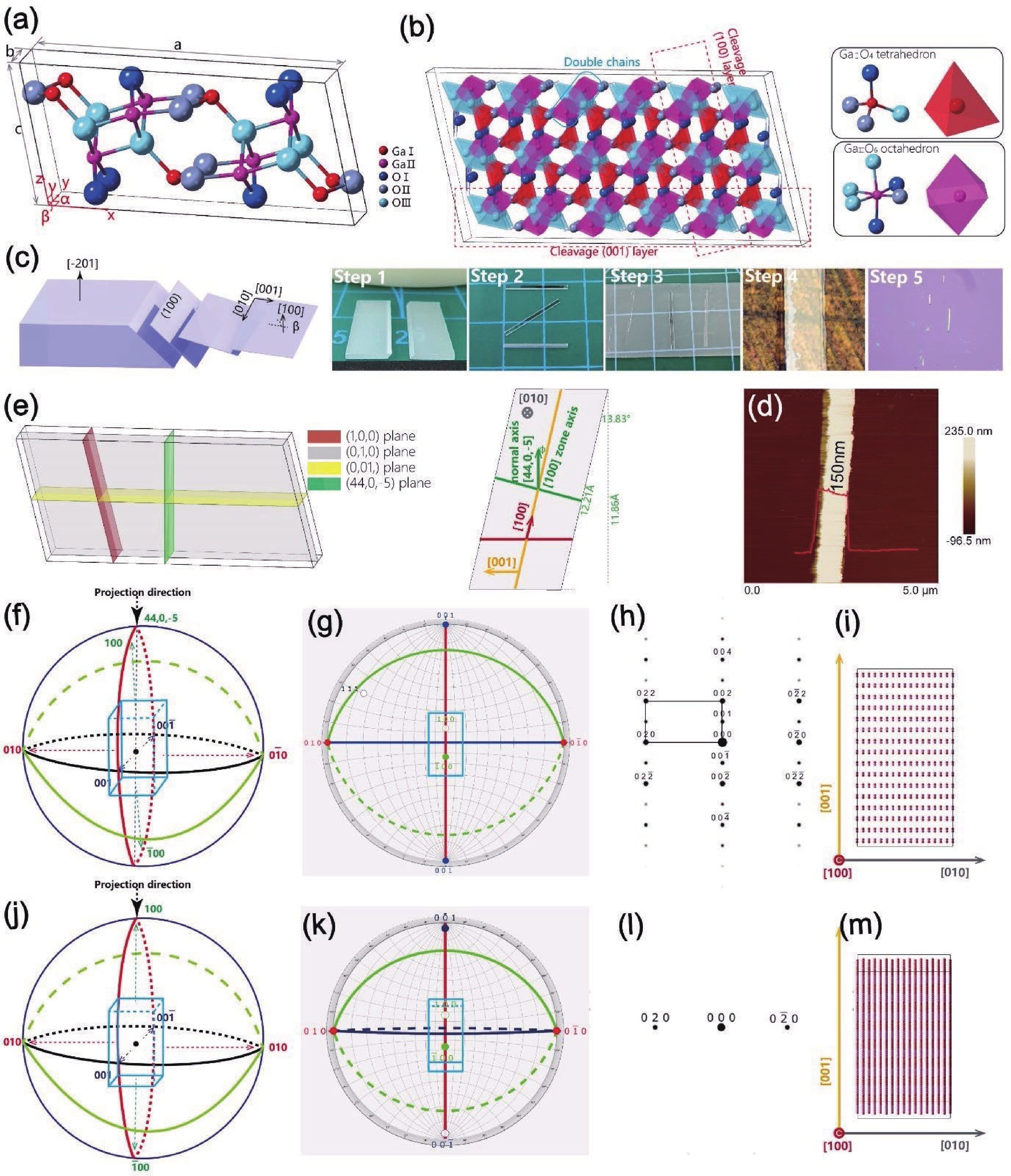
β-Ga2O3 is actually a reborn material, and related research can be traced back to 1960s[17, 18]. However, it is until recent ten years, especially from 2010, that β-Ga2O3 received growing attention from the area of power electronics and DUV optical devices. β-Ga2O3 has based-centered monoclinic lattice structure, which belongs to C2/m space group (space group number: 12), with inherent structure anisotropy[19]. Fig. 1(a) shows one unit-cell of β-Ga2O3, with an exceptional long base vector a of 12.21 Å, relatively short base vectors b of 3.04 Å and c of 5.80 Å. The α angle between x and y axes as well as the γ angle between y and z axes is right angle, while the β angle between x and z axes is 103.83°. There are two kinds of Ga3+ ions and three kinds of O2– ions in β-Ga2O3 crystal. As shown in Fig. 1(b), one kind of Ga3+, named Ga Ⅰ, occupies the distorted GaⅠO4 tetrahedral site, while the other kind of Ga3+, named Ga Ⅱ, occupies the distorted GaⅡO6 octahedral site. Both Ga Ⅰ and Ga Ⅱ ions are equal in quantity and both the GaⅠO4 tetrahedrons and GaⅡO6 octahedrons are aligned along [010] direction[20]. Band structure calculation[21] suggests that the anisotropic arrangement of GaⅠO4 tetrahedrons lead to the anisotropic electric and optoelectronic properties as will be discussed later in the following sections.

The anisotropic lattice structure of β-Ga2O3 renders the possibility of cleavage of thin flakes along x axis (the [100] direction) or z axis (the [001] direction)[22], since atoms are relatively weaker bonded in these directions compared to those in y axis (the [010] direction) where atoms are tightly bonded through the chains of GaⅠO4 tetrahedrons and GaⅡO6 octahedrons. As shown in Fig. 1(b), the GaⅡO6 octahedrons share edges to form double chains, furthermore the double chains are bonded together via GaⅠO4 tetrahedrons. All the three atom chains are parallel to y axis, leading to the intense covalent bonds along y axis[23]. Due to the huge difference in bonding strength between directions parallel and perpendicular to [010] direction, β-Ga2O3 can be easily exfoliated in (100) and (001) planes. In Fig. 1(c), the typical process flow of mechanical exfoliation is depicted. Step 1: the [−201] oriented β-Ga2O3 single crystal is manually broken into two parts, with cleavage plane of (100). Step 2: single-crystal slices of less than one millimeter thick can be peeled off from the bulk material. Step 3: the thickness of the slices can be reduced to few microns by riving with adhesive tape. Step 4: further reduce the thickness of β-Ga2O3 nanobelts to the thickness of tens to hundreds of nanometers. Step 5: dry-transfer the nanobelts onto substrate. The thickness of a typical nanobelt is measured with atomic force microscope (AFM) to be 150 nm [Fig. 1(d)].
For exfoliated β-Ga2O3 nanomaterials, (100) plane is the crystal plane to be used in many applications and characterizations. For clarity in analysis and calculation, it should be pointed out that, the [100] direction is not the normal direction of (100) plane[24] [Fig. 1(e)]. In addition, to accurately analyze the crystal structure, researchers should notice the difference between the concept of zone axis, in the crystal lattice, and the normal axis, in the laboratory coordinate system[25]. For (010) and (001) planes, it is easy to determine the zone axis [uvw] to be [100], according to the Weiss zone law,
| u=k1l1−k2l2,v=l1h2−l2h1,w=h1k2−h2k1, | (1) |
where (h1, k1, l1) = (010) and (h2, k2, l2) = (001). To figure out the normal axis of the (100) plane, that is the incident direction of optical characterizations, such as Raman scattering, photoluminescence and photodetector device applications, the included angles of crystal planes shall be calculated using
| cosϕ=d1d2sin2β[h1h2a2+k1k2sin2βb2+l1l2c2−(l1h2+l2h1)cosβac], | (2) |
where φ is the included angle between (h1, k1, l1) and (h2, k2, l2) crystal planes, d1 and d2 are crystal plane spacing of (h1, k1, l1) and (h2, k2, l2), a, b, c, β are the lattice constants as defined above. Assuming the index of the normal direction to be [h, k, l] and the interplane space to be d, for the two planes of (h, k, l) and (010),
| cos90∘=0 = dd(010)sin2β[0+ksin2βb2+0−0], | (3) |
for the two planes of (h, k, l) and (010),
| cos90∘=0=dd(001)sin2β[0+0+lc2−hcosβac], | (4) |
for the two planes of (h, k, l) and (100),
| cos13.83∘=dd(100)sin2β[ha2+0+0−lcosβac]. | (5) |
For monoclinic crystal structure, the crystal plane spacing d can be obtained via
| 1d2=h2a2sin2β+k2b2+l2c2sin2β−2lhcosβcasin2β. | (6) |
The orientation index [h, k, l] is calculated to be [44, 0, –5] by solving the above Eqs. (3)–(6).
If the projection direction is perpendicular to (100) plane [Fig. 1(f)], that is the typically vertical direction in the laboratory coordinate, the atoms are staggered arranged along [001] direction and cyclically arranged along [010] direction, as can be seen in Fig. 1(i). In the process of electron diffraction, electrons would be diffracted by atomic cores in the [44, 0, –5] plane [Fig. 1(g)], and diffraction pattern can be acquired as in Fig. 1(h). In another case, if the projection direction is along [100] direction [Fig. 1(j)], the atoms are arranged unordered along [001] and periodically along [010] direction from the view direction [Fig. 1(m)]. Accordingly, electrons are diffracted by atomic cores in the [100] plane [Fig. 1(k)], and a different diffraction pattern would appear as in Fig. 1(l).
Since high-quality β-Ga2O3 nanomaterials could be obtained via mechanically exfoliation, researchers have done intensive studies to apply β-Ga2O3 nanoflakes in various applications. Sooyeoun et al. reported metal-semiconductor-metal (MSM) photodetector by exfoliating [100] oriented β-Ga2O3 micro-flakes from bulk single crystal[24]. Li et al. reported large drain current β-Ga2O3 field-effect transistors with mechanically exfoliated β-Ga2O3 flakes[26]. The reported device performances using exfoliated β-Ga2O3 flakes are generally superior than others using bottom-up synthesis approaches, as the flakes inherit the high crystalline quality from the bulk single crystal. The innovativeness of exfoliation method is quite surprising since, unlike graphene and MoS2, β-Ga2O3 is not a conventional 2D layered material. The feasibility of layer-by-layer exfoliation results from the strong covalent bonding along [010] direction and relatively weak bonding along [100] and [001] directions. That is why β-Ga2O3 is often referred to as quasi-two-dimensional material[26–30]. The anisotropic crystal structure of β-Ga2O3 leads to the unique optical and electrical properties as will be discussed in the following sections.
3. Anisotropic optical properties
3.1 Anisotropic bandgap
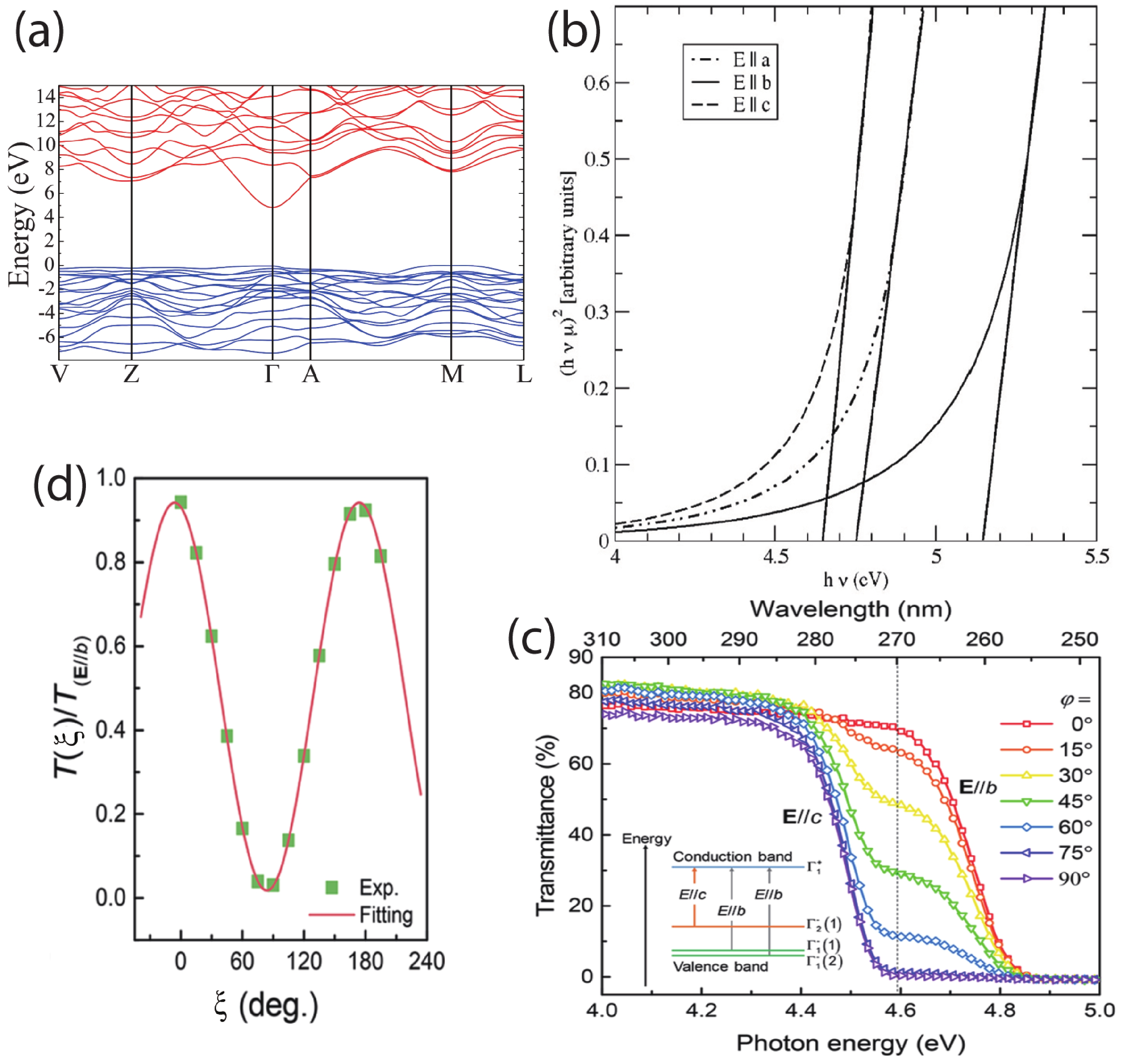
Due to the high anisotropic crystal structure, β-Ga2O3 features highly anisotropic optical properties, among which the anisotropic optical bandgap is the most in-depth studied one. The optical absorption edges for E//b and E//c polarized light were 4.79 and 4.52 eV, respectively, according to Ueda’s report[31]. It was also found that the rate of the band gap widening with increasing carrier concentration was much larger for E//b than E//c. It should be noted that, technically, β-Ga2O3 is an indirect-bandgap material with the minimum gap between the Γ point in conduction band minimum (CBM) and the M point in valance band maximum (VBM). However, since the valance band is quite flat and the M point is only a few meV higher than the Γ point in the valance band, the inter-band transition behavior is essentially that of a direct-bandgap material[32]. According to the first principle calculation, the CBM of β-Ga2O3, which mainly constituted by Ga 4s orbitals, is isotropic, while the VBM, constituted by oxygen 2p orbitals, is largely anisotropic[33, 34] [Fig. 2(a)]. The valance band minimum, which occurs just off the M point and is only 0.03 eV higher than at Γ, is set to zero on the energy axis. The absorption onsets of E//a, E//b and E//c polarized light are shown in Fig. 2(b). From the results for polarization parallel to the three crystallographic axes, one can draw the conclusion that the lowest absorption edge is along E//c, followed by the close onset of E//a, while E//b gives the obvious highest onset value. The absorption coefficient is plotted in Tauc form with exponent of 2, indicating that researchers treated β-Ga2O3 as a direct bandgap material although its bandgap is indirect in nature. It is clear to see that there is approximately 0.5 eV difference in the optical bandgap between the cases of E//b and E//c. Chen et al. reported the polarized transmittance characteristics of β-Ga2O3 single crystal, and revealed the transitions from valance subbands to the CBM which is tuned between 4.54 to 4.76 eV for 0° to 90° polarization between E//c and E//b[35] [Fig. 2(c)]. The angle resolved transmittance verifies that the band-to-band transitions obey well the selection rules in terms of the valence-band splitting in the β-Ga2O3 monoclinic crystal band structure. The angle dependence transmittance power at 4.6 eV can be expressed as T(ξ) = TE//bsin2(ξ) + TE//ccos2(ξ), where the in-plane polarization angle ξ is defined as the angle between the b axis and the electric field vector E and TE//b and TE//c represent the transmittance magnitudes for the cases of ξ = 0° and 90° at 4.6 eV, respectively [Fig. 2(d)].

Yamaguchi reported[34] the irreducible representations of the eigen-functions of band levels at Γ point in 2004, in which, the CBM state at Γ belongs to Γ+1, while VBM, the 55th and 56th states belong to Γ−2. The transition of polarized dipoles along x (E//a) and z (E//c) directions are allowed by the selection rule of 56th and 55th state (at Γ−2 point) to 57th state (at Γ+1 point), respectively. While the transition of polarized dipoles along y (E//b) direction is allowed by the selection rule of 51st and 52nd states (at Γ−1 point) to 57th state. According to the group theory, the direct transition from Γ+1 and Γ+2 are forbidden. Therefore, the optical bandgap is expected to be related merely to the VBM at Γ−1 and Γ−2 which is about 0.67 eV lower beneath it, disregarding the existence of Γ+1 and Γ+2 states. The drop difference from the 56th to the 52nd states are 0.67 eV, which is in good consistency with the anisotropic bandgap difference from other papers listed in Table 1. It should be noted that there is distinct bandgap order for the three polarization directions, that is E||c < E||a < E||b. Theoretical calculation indicates the energy ordering is actually due to suppression of the transition matrix elements of three top valence bands[33].
 DownLoad:
CSV
| Show Table
DownLoad:
CSV
| Show Table
3.2 Raman scattering and Raman tensor
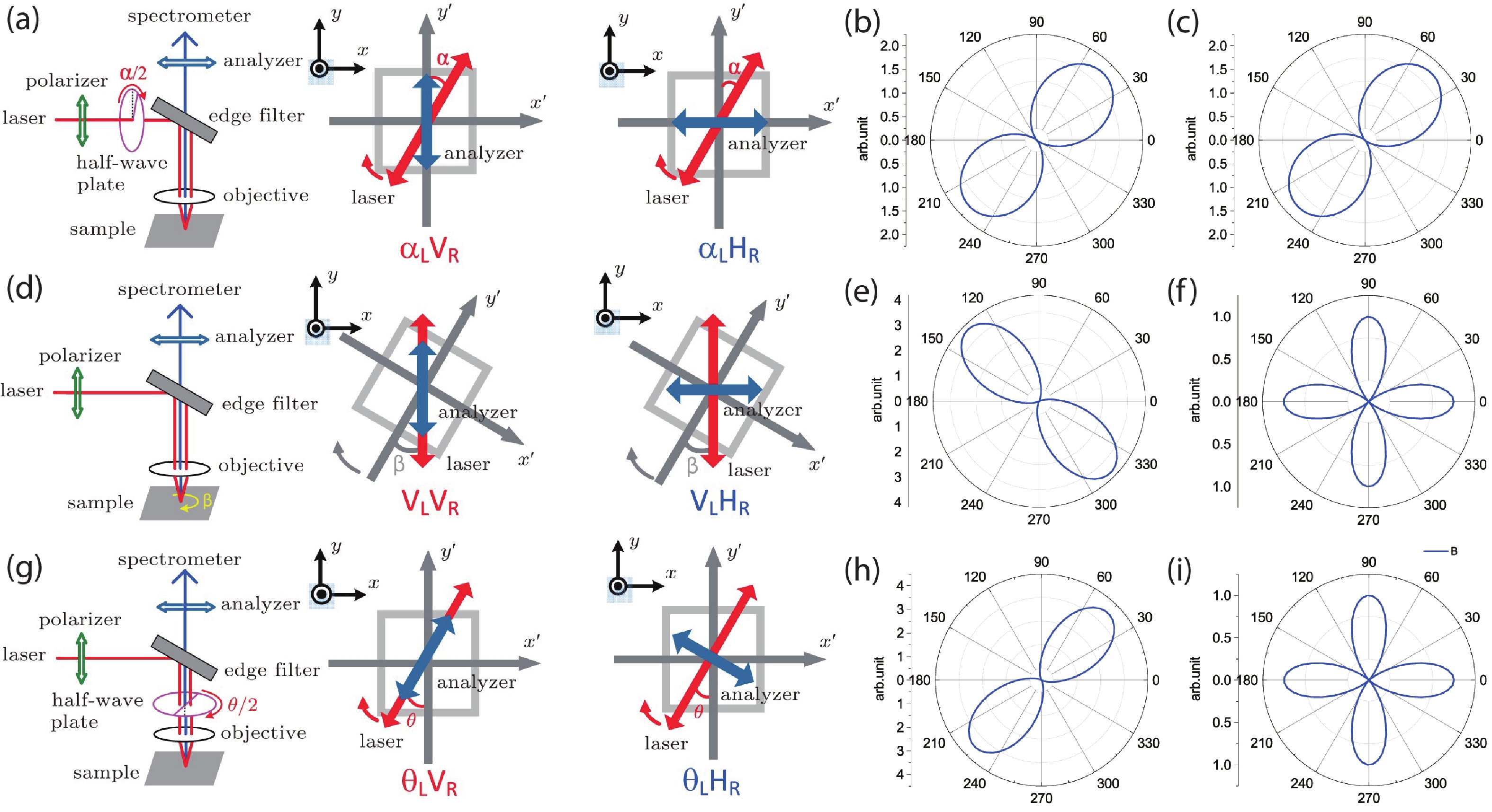
Raman scattering technique is generally employed in condensed matter physics for nondestructive-probing of crystal’s phonon mode and lattice dynamics. Since the behavior of electrons, phonons and their coupling influence the optical and electrical properties of β-Ga2O3, Raman spectroscopy has been proven to be an effective and non-destructive testing tool. In addition, due to the high anisotropy of β-Ga2O3 single crystal, angle-resolved polarized Raman spectroscopy (ARPRS) is utilized in studying the anisotropic physical properties. ARPRS features periodically varied Raman intensity for each of the vibration modes, which is directly related to the corresponding Raman tensor elements. Despite the same physical connotation, ARPRS measurement could be operated in several configurations, thus lead to different results and analyzing processes. Liu et al. summarized three typical ARPRS measurement configurations as illustrated in Fig. 3[25].

Type 1: Vary the angle of the incident light, while keep the sample steady
This configuration, as shown in Fig. 3(a), is the most commonly used one as it is time-saving and easy-to-operate. At the beginning, the polarization angle of the incident light is in consistence with y axis. By simply rotating the fast axis of the half-wave plate, which is placed in the incident laser beam path, with an angle of α/2, the polarization angle of the incident light rotates with an angle of α from the y axis. Since the objective sample is stationary, the angle between the polarization direction and the sample could be modulated accordingly. The intensity of the ARPRS spectra can be fitted with Raman tensor through the equation[25]
| I∝∑j|eR⋅Rj⋅eL|2, | (7) |
where eR and eL are the unit polarization vector of the Raman signal and the incident beam, Rj is a 3 × 3 Raman tensor. The overall Raman intensity is the sum of the polarized Raman signal, along eR, which is twisted by the Raman tensor from eL. Generally, the Raman tensor is composed with nine independent numbers, for instance, a to g.
| Rj=(abcdefghi). | (8) |
From Bilbao Crystallographic Server[38], researchers can find the characteristic Raman tensors of materials according to their space group. For β-Ga2O3, space group C2/m (No. 12), under non-resonant condition, the Raman tensors can be simplified in the form[39]
| Ag:Rj=(ad0db000c);Bg:Rj=(00e00fef0). | (9) |
The polarization of the incident laser, eL, can be expressed in the form eL = (sinα cosα 0), where α is the angle between the polarization direction and the y’ axis of the laboratory coordinate as shown in Fig. 3(a). The polarization direction of the analyzer is fixed either parallel or vertical to the y’ axis with unit vector eR = (010) and (100), respectively. The overall Raman intensity in this configuration can be calculated via
| I=|(0 1 0)(ad0db000c)(sinαcosα0)|2=|dsinα+bcosα|2. | (10) |
If the polarization direction of the analyzer is set along x’, that is eR = (100), the overall Raman intensity in this configuration can be calculated via
| I=|(1 0 0)(ad0db000c)(sinαcosα0)|2=|asinα+dcosα|2. | (11) |
The polar plots of β-Ga2O3 ARPRS in this configuration with eR = (010) and eR = (100) are shown in Figs. 3(b) and 3(c), respectively. The Raman tensor elements can be acquired by fitting the ARPRS intensity using Eqs. (10) and (11).
Type 2: Rotate sample while keep the incident laser unchanged
The second measurement configuration, as shown in Fig. 3(d), is to rotate the sample while keep the polarization direction of the incident laser unchanged. In this case, the unit polarization vector eR and eL is fixed, and the Raman tensor Rj is modified as Rj is defined in crystal coordinates which is rotated in this configuration. The converted Raman tensor Rj’ can be expressed as
| R′j=M⋅Rj⋅MT, | (12) |
| M=(cosβsinβ0−sinβcosβ0001), | (13) |
where M is a rotating matrix, and β is the angle between the crystal coordinate and laboratory coordinates.
For the case that both the incident laser and the analyzer polarized along y’ axis, the intensity of the Raman signal could be calculated via
| I=∑j|eR⋅M⋅Rj⋅MT⋅eL|2=|(010)(cosβsinβ0−sinβcosβ0001)(ad0db000c)(cosβ−sinβ0sinβcosβ0001)(010)|2=|asin2β+bcos2β−2dsinβcosβ|2. | (14) |
For the case that the incident laser polarized along y’ axis while the analyzer along the x’ axis, the intensity of the Raman signal could be calculated via
| I=∑j|eR⋅M⋅Rj⋅MT⋅eL|2=|(100)(cosβsinβ0−sinβcosβ0001)(ad0db000c)(cosβ−sinβ0sinβcosβ0001)(010)|2=|d(cos2β−sin2β)+(b−a)sinβcosβ|2. | (15) |
The polar plots of β-Ga2O3 in this configuration with eR = (010) and eR = (100) are shown in Figs. 3(e) and 3(f), respectively.
Type 3: Vary eR and eL simultaneously
The third measurement configuration, as shown in Fig. 3(g), is to vary eR and eL simultaneously by adjusting the half-wave plate inserted in the optical path between Raman filter and microscope objective. Jones matrix[40] Jλ/2 is involved to quantify the influence of optical devices on polarized light.
| Jλ/2 = (−cosθsinθ0sinθcosθ0000). | (16) |
The polarization eL of the incident laser is modified by the half-wave plate via e’L= Jλ/2∙eL, and eR via e’R= eR∙Jλ/2. The overall Raman intensity in this configuration can be calculated with
| I=∑j|eR⋅J⋅Rj⋅J⋅eL|2. | (17) |
For analyzer polarized along y’ axis, the intensity can be calculated via
| I=∑j|eR⋅J⋅Rj⋅J⋅eL|2 = |(010)⋅(−cosθsinθ0sinθcosθ0000)⋅(ad0db000c)⋅(−cosθsinθ0sinθcosθ0000)⋅(010)|2 = |asin2θ+bcos2θ + 2dsinθcosθ|2. | (18) |
For analyzer that polarized along x’ axis, the intensity can be calculated via
| I=∑j|eR⋅J⋅Rj⋅J⋅eL|2 = |(100)⋅(−cosθsinθ0sinθcosθ0000)⋅(ad0db000c)⋅(−cosθsinθ0sinθcosθ0000)⋅(010)|2 = |dsin2θ−dcos2θ+(b−a)sinθcosθ|2. | (19) |
The polar plots of β-Ga2O3 in this configuration when the analyzer is vertical and horizontal to the incident laser direction are shown in Figs. 3(h) and 3(i), respectively. The practical curvature of the above polar plots may differ in each phonon mode as they depend on the value of a/b/d Raman tensor elements, however the fundamental characteristics remain.
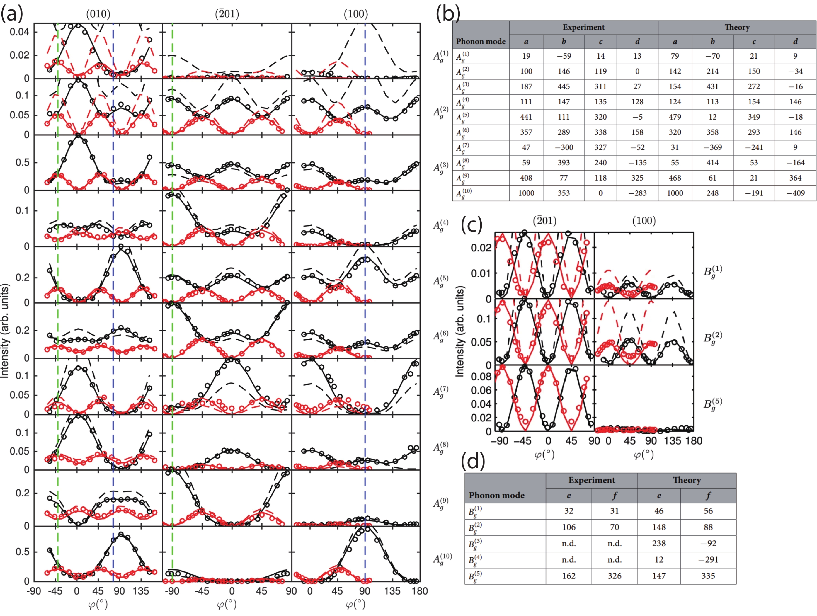
For Bg modes, the ARPRS intensity can be calculated through similar process with Bg Raman tensor elements. To save space of this paper, the calculation part of Bg modes will not be shown here. With the above theoretical calculation, researchers could work out the Raman tensor elements of each of the phonon modes by fitting the ARPRS results with corresponding equations. Kranert et al. have reported ARPRS for Ag and Bg modes as shown in Figs. 4(a) and 4(c), and worked out an entire set of Raman tensor elements [Figs. 4(b) and 4(d)][39]. The spectral position of all 15 Raman active phonon modes and the Raman tensor elements of 13 modes were determined and the Raman tensor elements were found in good agreement with the results from ab-initio calculations.

3.3 Anisotropic photoluminescence properties
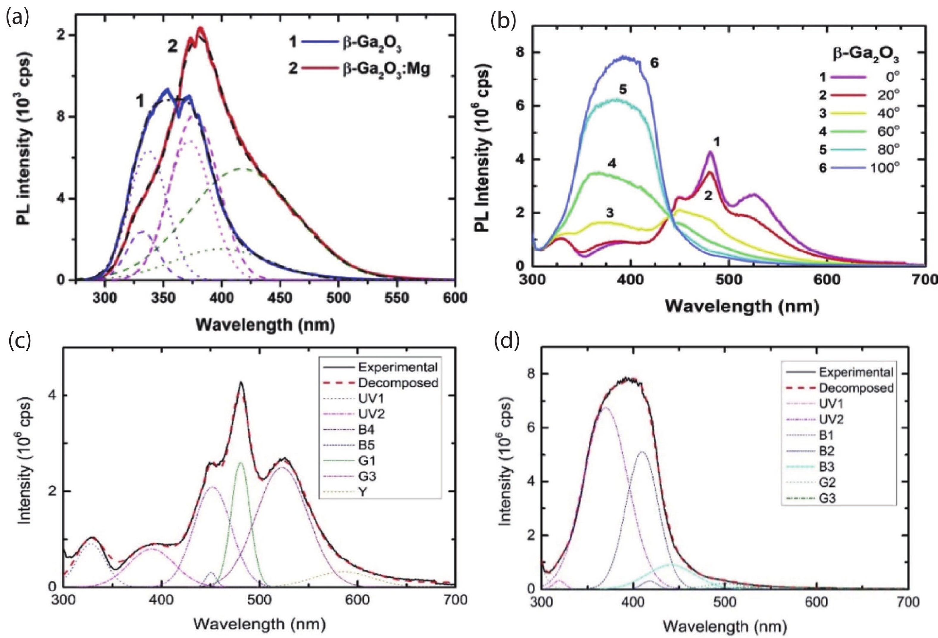
The photoluminescence spectra of β-Ga2O3 can be decomposed into three main bands, according to Zhang et al.’s report[37]. The first band at 330 nm is originated from phonon-assisted transition from CBM to self-trapped holes (STH), while the second and third ones at 380 and 400 nm are the sign of free electron detachment by STH at VO donor positions[41] [Fig. 5(a)]. They also found a strong anisotropic behavior of the PL spectra in β-Ga2O3 as can be seen in Fig. 5(b). In the case of 0° polarization angle [Fig. 5(c)], that is along [001] direction, the PL spectrum can be decomposed into seven bands from UV to yellow. In contrast, there are different peak positions and proportion for the case of 100° polarization direction [Fig. 5(d)], that is along [010] axis. The intensity of the two UV bands are enhanced along the [010] direction, as they are determined by the spatial distribution of STH which are preferable at oxygen sites[42]. Since the O1, O2, O3 sites are aligned in rows along [010] direction as can be seen in Fig. 1(b), the UV luminescence is stronger in 100° polarization. The two blue band, B4 and B5 at 450 and 452 nm, decreased with the polarization angle and disappeared at 100°. The variation of B4 and B5 bands indicates the change of vacancies located at Ga-sites: (VGa1 + VO1) and VGa2, which seem to have different electron density distribution and specific dipole moments orientation of recombination transitions more likely closer to the [001] than to the [010] direction.

4. Anisotropic electronic properties
In recent years, β-Ga2O3, as an ultra-wide band gap semiconductor (Eg = 4.9 eV at room temperature) with excellent electrical performance, has gained much attention in preparing high-voltage devices. To better understand the excellent electrical properties of β-Ga2O3, the key parameters of β-Ga2O3 are compared with those of GaN (typical 3rd-generation-semiconductor) and Si (the 1st-generation-semiconductor) materials in Table 2. β-Ga2O3 has better performance in high-voltage electricity than GaN and Si, as its ultra-wide band gap renders the breakdown field strength as high as 8 MV/cm, which is 2.4 times that of GaN and more than 10 times that of Si based devices. Meanwhile, the saturation electron drift velocity of β-Ga2O3 is as high as 2.4 × 107 cm/s, and its Baliga’s figure of merit (the key parameter characterizing power device materials) is as high as 3444, which is far higher than the merit value of GaN (846) and SiC (277), the mainstream wide-band gap materials used in power devices at present. Yang et al. reported the vertical structure Schottky diode of Ga2O3:Si with a reverse breakdown voltage of 2300 V[43], and Wong et al. also reported the Si ion implanted Ga2O3 MESFET with a breakdown voltage of 755 V[44]. β-Ga2O3 is proved to be one of the most valuable material for next generation power electronics.
| Parameter | Eg (eV) | Ebr (MV/cm) | Velocity (107 cm/s) | K (W/(cm·K)) | Y (GPa) |
| AlN | 6.2 | 17 | 2.2 | 2.9 | 310 |
| Diamond | 5.5 | 10 | 2.7 | 10 | 1100 |
| β-Ga2O3 | 4.9 | 8 | 2.4 | 0.27 | 230 |
| GaN | 3.4 | 3.3 | 2.5 | 2.1 | 336 |
| Si | 1.12 | 0.5 | 1 | 1.56 | 130 |
DownLoad:
CSV
| Show Table
β-Ga2O3 belongs to monoclinic crystal structure with low symmetry. Along the b-axis, Ga atoms are most closely arranged with interplanar spacing of 3.031 Å. Therefore, the electron cloud of Ga 4s orbital overlapped more along b-axis than other directions, resulting in about 18 times higher mobility in this direction than that of c-axis[31]. The anisotropic mobility can be understood by comparing the effective mass along b and c axis. The effect mass can be calculated via
| 1m∗vc=1m∗v+1m∗c, | (20) |
| m∗=[1ℏ2(∂2E(k)∂k2)]−1, | (21) |
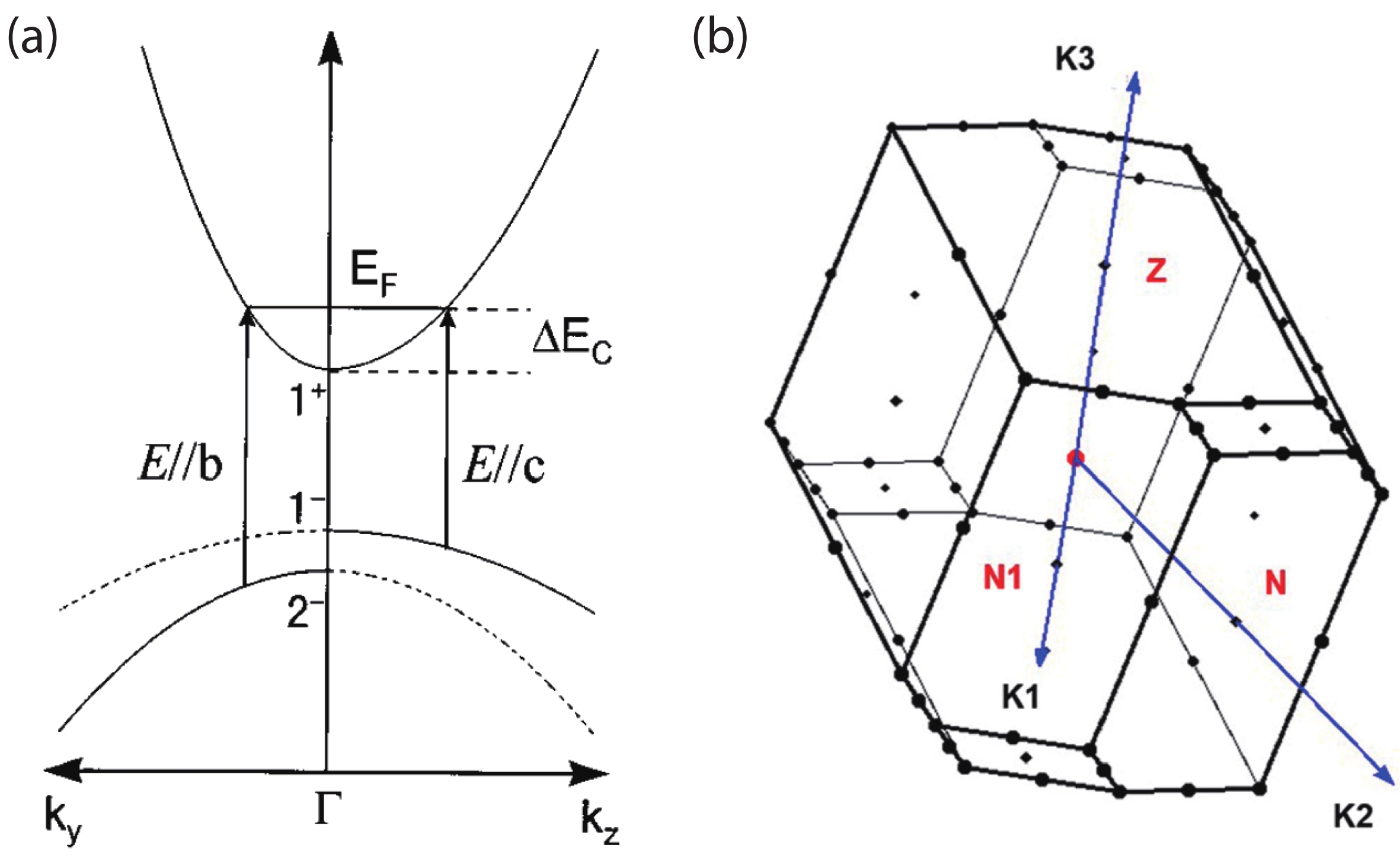
where m∗, m∗vc, m∗v and m∗c are the general effective mass, reduced effective mass, valence band effective mass and conduction band effective mass, respectively. E(k), k and ћ are the electron energy, wave vector and reduced Planck constant. The schematic diagram of the band structure of β-Ga2O3 along wave factor ky and kz is shown in Fig. 6(a). The reduced effective mass m∗vc for E//b and E//c is estimated to be (0.44+0.33−0.14)m0 and (1.24+0.15−0.11)m0, respectively. This is due to the fact that the amount of energy shift experienced by the conduction band, ΔEC, is identical in all directions even though the curvature of the conduction band is different. On the other hand, the curvature anisotropy of the valence band of the initial states affects the difference of the band gap widening for the orientation of polarization. Since the upper valance band is flatter than the lower one, the m∗v of the Γ−1 band along kz, along c, is heavier than that of the Γ−2 band along ky (along b), thus leading to higher electron mobility along b axis.

Carrier mobility is an important parameter to measure the electrical performance of semiconductors, which affects the conductivity, working speed and calorific value of electronic devices. In addition, the primitive cell of β-Ga2O3 is relatively large with 10 atoms, resulting in as many as 30 phonon modes. For comparison: there are 2 atoms in one primitive cell and 6 phonon modes in silicon. The magnitude of phonon modes and low symmetry lattice structure lead to complex phonon-electron coupling in β-Ga2O3[45].
In addition, the electron–phonon coupling would induce different influence on the transport properties of β-Ga2O3 under low and high electric-fields circumstances. The thermal vibration of the lattice would superimpose perturbation on the periodic potential field, however, the perturbation itself is isotropic and will not lead to anisotropic transport of carriers. On the other hand, as the combination of Ga atoms and O atoms in β-Ga2O3 contains some ion-bond components, the vibration of the net dipole moment of the ion-bond will superimpose another electron-phonon interaction. This electron phonon interaction is the coupling of electrons and polarized optical phonons (Bu1 mode), which is essentially a long-range Coulomb interaction and mainly affects the electron transportation in low-electric fields. According to theoretical calculations, it is the anisotropic electron-phonon coupling that leads to the anisotropic mobility of β-Ga2O3 in low electric field[46]. Resulting from the highly anisotropic crystal structure, the Brillouin zone of β-Ga2O3 is anisotropic as well [Fig. 6(b)]. In the case of low-field, the electrons are with low-energy and mainly occupy the center of Brillouin region near the Γ point. The electronic structure near the Γ point is almost isotropic and will not result in the anisotropic transport of carriers. In the case of high-electric field, the electrons are with high-energy and will locate at the boundary of the Brillouin zone. The high-energy electrons will have a short-range interaction with the Bu6 phonon, whose energy is higher than that of Bu1 phonon’. Since the short-range interaction is a key factor affecting the saturation transportation speed in high-electric field, the transportation properties of electrons of β-Ga2O3 in high electric fields must differ from those in low-electric fields. Despite the lack of experimental report, there are some theoretical studies on the anisotropic mobility on anisotropy performance of β-Ga2O3 power devices. Li et al. included the anisotropic mobility modeling in calculating the electrical performances of β-Ga2O3 (001) power device[47]. The effect of the anisotropic mobility model on the on-state characteristics and reverse recovery are examined, enabling a more accurate prediction of device performance.
The value of electron affinity of β-Ga2O3 from the literature is quite broad, ranging from 2.5 eV[8] to more than 4 eV[7, 48]. The reason can be ascribed, on the one hand, to the effect of different preparation methods, sample morphology and characterization conditions. On the other hand, it is due to the low symmetry of monoclinic crystal system, which leads to different electron affinity on different crystal planes. However, many reports have not taken the difference of crystal planes into account. According to the metal-semiconductor-contact theory, the electron affinity of semiconductor materials affects the contact type and Schottky barrier height (SRH) of electrodes, and the electrode contact performance is extremely important for any device. Therefore, it is also of great significance to study the electrical performance differences between different crystal planes of β-Ga2O3.
5. Applications based on anisotropic properties of β-Ga2O3
5.1 Polarization photodetector
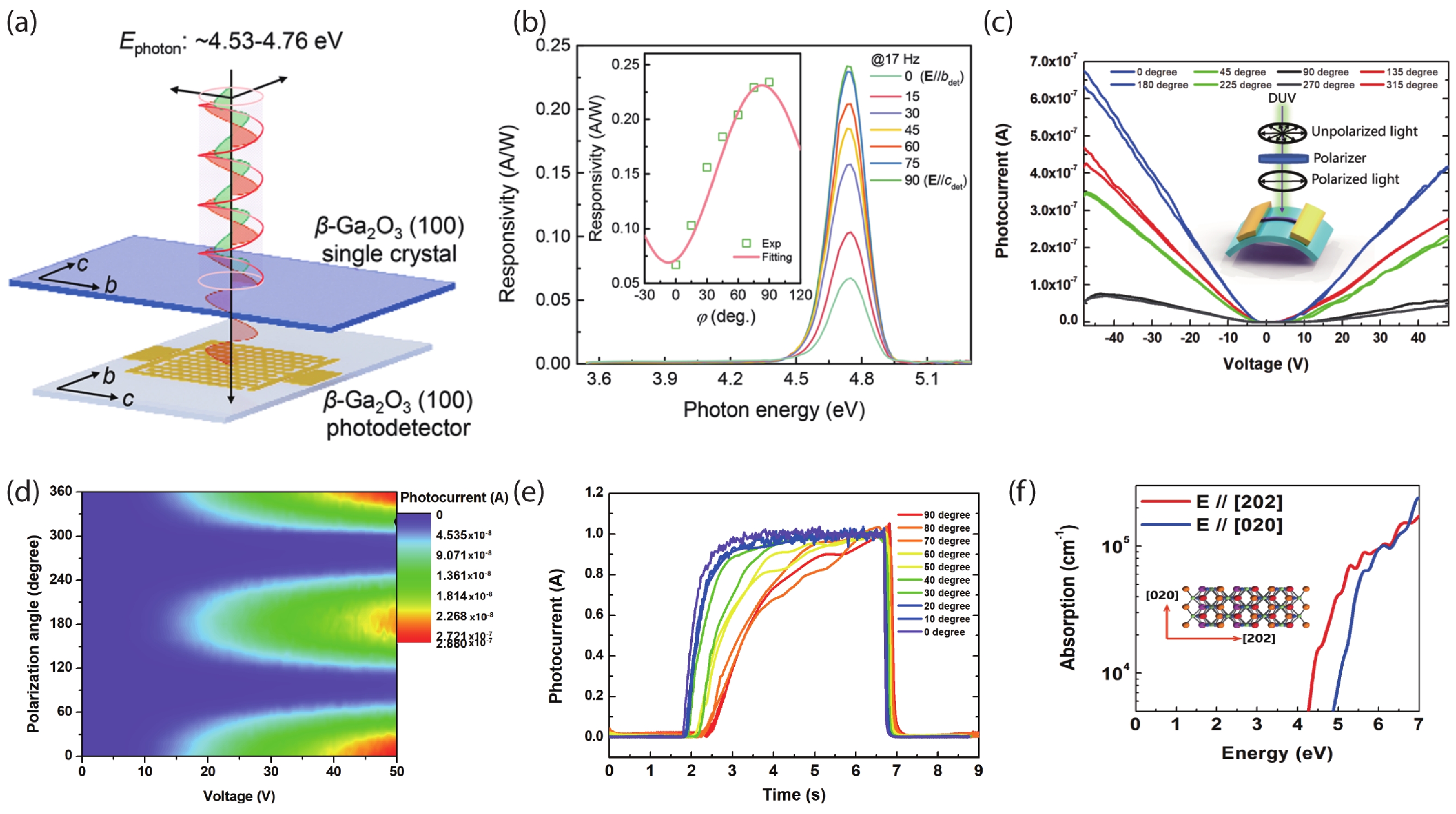
The detection of the polarization state in DUV wavelength is of tremendous importance, particularly, in free space ultraviolet (UV) communication[49]. In our previous work[50], the polarization detectors can be categorized into three types according to their detection mechanisms. The first one is called “dichroism”, which means the polarization selectivity is derived from the intrinsic anisotropic optical properties that are related to their anisotropic crystal lattices. Actually, six among the seven crystal systems are expected to be anisotropic, except for cubic crystals[19]. Chen et al. reports polarization-sensitive solar-blind photodetectors based on β-Ga2O3 (100) single crystals[35]. They report strong polarized transmittance characteristics [Fig. 2(c)] and light polarization-controlled responsivity for the incident light polarized E//c and E//b. The schematic diagram of the polarization photodetector is shown in Fig. 7(a), with one (100) single crystal plate above the photodetector device. Since the above single crystal plate is with polarization selectivity like a polarizer, the light that irradiated onto the device varied with the polarization angle of the incident light. The maximum response is sensitive to the polarization angle of incident light, which can be well described by the relation R(φ) = RE//csin2(φ) + RE//bcos2(φ) as shown in the inset of Fig. 7(b). Our group first reported polarization photodetector based on single-crystal β-Ga2O3 nanobelts in 2020[50] [Fig. 7(c)]. Different from Chen’s report, the working mechanism depends on the intrinsic optical anisotropy. The photoresponsivity [Fig. 7(d)] and response speed [Fig. 7(e)] for E//[202] are higher than that for E//[020], which was ascribed to the higher absorbance [Fig. 7(f)] for E//[202] polarized light.
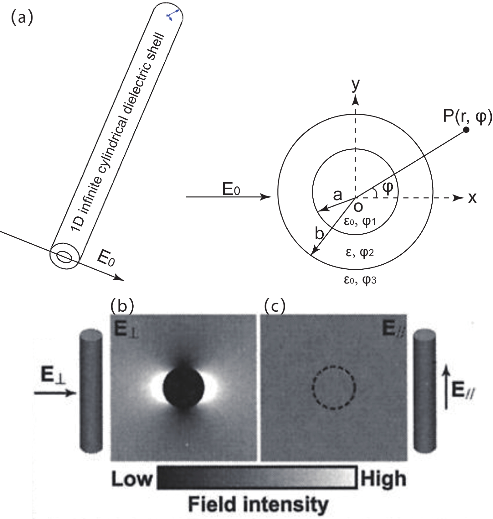
The second type is referred to as “morphology”, as the detection mechanism is related to the attenuated electric field that results from the large dielectric contrast between 1D materials (nanowires, nanorods and nanobelts) and the surrounding environment[51].
Supposing an infinite cylindrical dielectric shell as in Fig. 8(a), with inner diameter a, outer diameter b and dielectric constant of ε, in uniform electric field E0, the Laplace equation and boundary condition can be written as

| ∇2ϕ1=0,r<a, | (22) |
| ∇2ϕ2=0,a⩽ | (23) |
| {\nabla ^2}{\phi _3} = 0,\quad r > b , | (24) |
| {\phi _1} = \text{Finit\ value}{\text{ }},\quad r = 0 , | (25) |
| {\phi _1} = {\phi _2},{\text{ }}{\varepsilon _0}\frac{{\partial {\phi _1}}}{{\partial \varphi }} = \varepsilon \frac{{\partial {\phi _2}}}{{\partial \varphi }},\quad r = a , | (26) |
| {\phi _2} = {\phi _3},{\text{ }}\varepsilon \frac{{\partial {\phi _2}}}{{\partial r}} = {\varepsilon _0}\frac{{\partial {\phi _3}}}{{\partial r}},\quad r = b . | (27) |
Since the electric filed E is symmetric on both sides of the x axis, the potential Φ is an even function of angle φ. The potential in different area can be written as
| {\phi _1} = \sum\limits_{n = 1}^\infty {({B_n}{r^n} + {D_n}{r^{ - n}})\cos n\varphi },\quad r < a, | (28) |
| {\phi _2} = \sum\limits_{n = 1}^\infty {({B'}_n{r^n} + {D'}_n{r^{ - n}})\cos n\varphi },\quad a \leqslant r \leqslant b, | (29) |
| {\phi _3} = \sum\limits_{n = 1}^\infty {({B{''}}_n{r^n} + {D{''}}_n{r^{ - n}})\cos n\varphi }, \quad r > b. | (30) |
By solving the above equations using the Laplace equations and boundary conditions, the express of the potential is solved to be
| {\phi _1} = - \frac{{4{\varepsilon _{\rm r}}}}{{{{({\varepsilon _{\rm r}} + 1)}^2} - {a^2}{b^{ - 2}}{{({\varepsilon _{\rm r}} - 1)}^2}}}{E_0}r\cos \varphi,\quad r < a, | (31) |
| \begin{split} {\phi _2} =& \left[ - \frac{{2({\varepsilon _{\rm r}} + 1)}}{{{{({\varepsilon _{\rm r}} + 1)}^2} - {a^2}{b^{ - 2}}{{({\varepsilon _{\rm r}} - 1)}^2}}}r -\right.\\ &\left.\frac{{2{a^2}({\varepsilon _{\rm r}} - 1)}}{{r{{({\varepsilon _r} + 1)}^2} - {a^2}{b^{ - 2}}{{({\varepsilon _{\rm r}} - 1)}^2}}}\right]\cos \varphi ,\quad a \leqslant r \leqslant b, \end{split} | (32) |
| {\phi _{\text{3}}} = \left[ - {E_0}r + \frac{{({\varepsilon _{\rm r}} + 1)({\varepsilon _{\rm r}} - 1)({b^2} - {a^2}){E_0}}}{{r{{({\varepsilon _{\rm r}} + 1)}^2} - {a^2}{b^{ - 2}}{{({\varepsilon _{\rm r}} - 1)}^2}}}\right]\cos \varphi, \quad r > b. | (33) |
For one-dimensional infinite cylinder, such as nanowires and nanobelts, the inner diameter a is reduced to 0. Eqs. (32) to (33) can be transformed into
| {\phi _2} = - \frac{2}{{{\varepsilon _r} + 1}}{E_0}r\cos \varphi, \quad r \leqslant b, | (34) |
| {\phi _{\text{3}}} = \left[ - {E_0}r + \frac{{({\varepsilon _r} - 1){b^2}{E_0}}}{{r({\varepsilon _r} + 1)}}\right]\cos \varphi,\quad r > b. | (35) |
The electric field E can be calculated via {E_2} = - \nabla {\phi _2} to be
| {E_2} = \frac{2}{{{\varepsilon _r} + 1}}{E_0} = \frac{{2{\varepsilon _0}}}{{\varepsilon + {\varepsilon _0}}}{E_0},\quad r \leqslant b. | (36) |
When the incident field is polarized parallel to the cylinder, the electric field inside the cylinder is not reduced [Fig. 8(c)]. But when polarized perpendicular to the cylinder, the electric field amplitude is attenuated according to Eq. (36)[51], as can be seen in Fig. 8(b). The above derivation process is simplified with infinite model, which does not exist in reality. In practice, nanowires should be as thin as possible to suit the model. Finer 1D materials are preferred to increase the anisotropy. Generally, the diameter of 1D materials should be much smaller than the excitation wavelength, while the crystallinity is not a key factor. We reported polarization photodetectors based on β-Ga2O3 nanobelts, and ascribed the high anisotropic ratio to the combination of intrinsic dichroism and 1D morphology mechanisms[50].
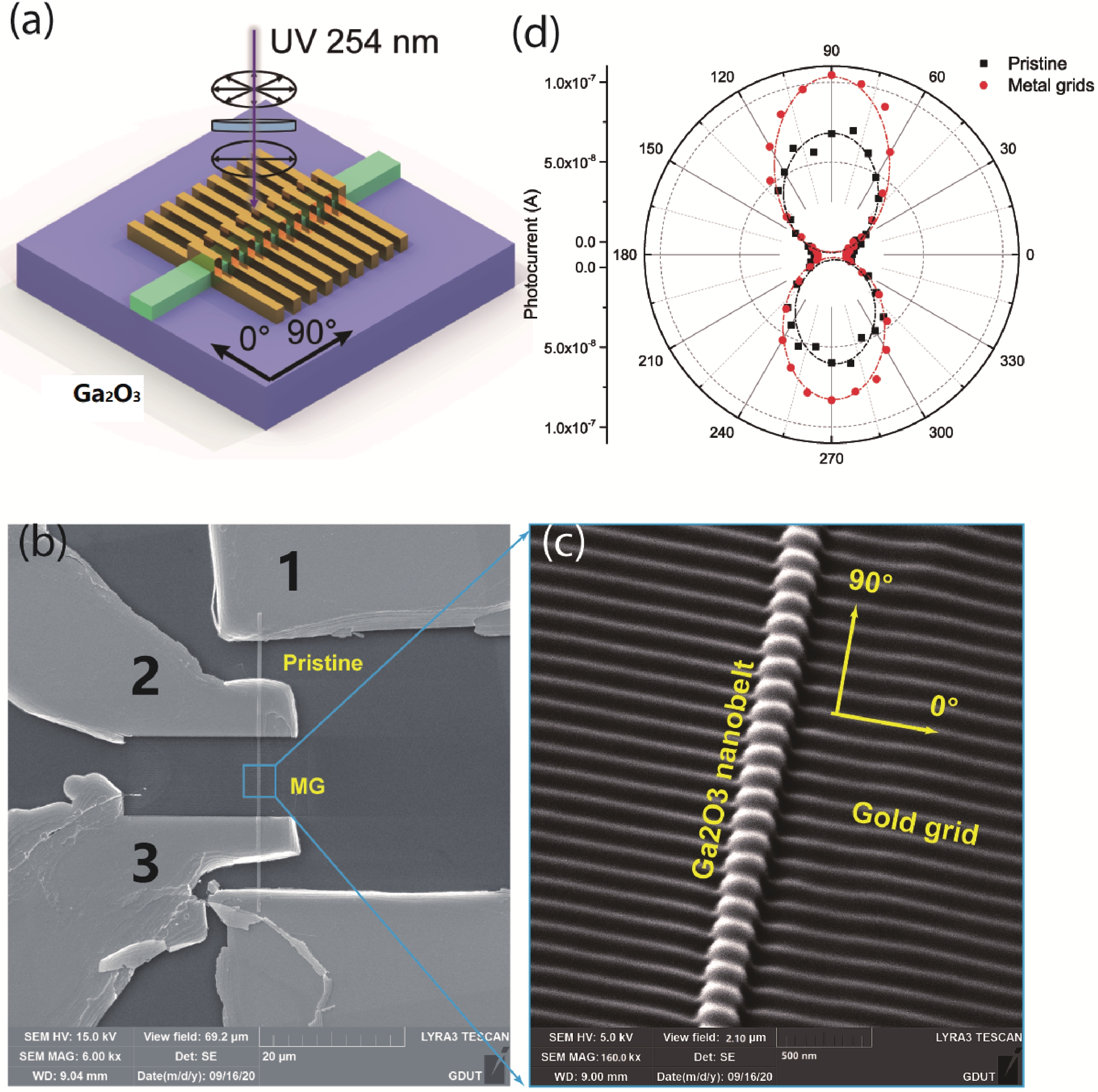
The third type is referred to as “metal-grid (MG)”, which means the detection requires sub-wavelength metal-grids on the active area. Plasmonic meta-surfaces at sub-wavelength scale, at most one-fifth of the wavelength, are found to function as a polarizing mirror or a polarizer[52, 53]. In addition, sub-wavelength metal grids were integrated with photodetectors to construct focal plane polarization photodetectors[54, 55]. Our group reported enhancement of polarization response in UVA and UVC wavelength by placing sub-wavelength Au grids onto β-Ga2O3 and wurtzite-ZnO materials (Fig. 9)[56]. Au metal-grids, as can be seen in Fig. 9(c), is fabricated with FIB technology and integrated with monoclinic Ga2O3 nanobelts photodetector, bringing about improved polarization rejection ratio from 7.5 to 49 (Fig. 9(d)).
Polarization detection based on monoclinic, triclinic, hexagonal, orthorhombic and tetragonal materials has been summarized in Table 3. β-Ga2O3 based deep-ultraviolet polarization photodetectors emerged since recent years. In Table 3, there are some of the reported works on polarized photodetectors. Most of the works are based on the dichroism properties of the semiconductor material, with less reports based on the attenuated electric field in 1D nanomaterials and few based on metal-grids meta-surfaces. β-Ga2O3 and β-GaxInyO3 are two kinds of material that have been demonstrated in polarization detection in the UVC range. GaN, ZnO, GeS2 and SnO2 are utilized in the UVA range due to their relatively small bandgap energy. Monoclinic, hexagonal, orthorhombic, tetragonal and triclinic crystal structures are proven to have intrinsic dichroism. Actually, six among the seven crystal systems are expected to be anisotropic, except for the cubic system, which can possess dichroism properties with 1D morphology as well.
| Material | Crystal system | Anisotropic plane | Optical bandgap (eV) | Detection wavelength | Material morphology | Anisotropic mechanism | Anisotropy ratio | Ref. |
| β-Ga2O3 | Monoclinic | (−101) | 4.8 | UVC | 3D Nanobelt | Dich. & Morp. & MG | 0.96(#) | [56] |
| β-Ga2O3 | Monoclinic | (−101) | 4.8 | UVC | 3D Nanobelt | Dichroism | 0.96(#) | [50] |
| β-Ga2O3 | Monoclinic | (100) | 4.53-4.76 | UVC | 3D Bulk | Dichroism | 0.53(*) | [35] |
| β-GaxIny03 | Monoclinic | (010) | 4.4−4.7 | UVC | 3D Bulk | Dichroism | − | [57] |
| GeS2 | Monoclinic | (001) | 3.71 | UVA | 2D flake | Dichroism | 0.36(#) | [58] |
| SnO2 | Tetragonal | (010) | 3.6 | UVA | 3D Microwire | Dichroism | 0.39(#) | [59] |
| MZO/ZnO-MQW | Hexagonal | (11−20) | 3.17−3.57 | UVA | 3D MQW | Dichroism | 0.71(#) | [60] |
| ZnO | Hexagonal | (0001) | 3.37 | UVA | 3D Thin film | MG | [56] | |
| ZnO | Hexagonal | − | 3.37 | UVA | 3D Nanowire | Morphology | 0.19(*) | [61] |
| GaN | Hexagonal | (11−20) | 3.4 | UVA | 3D Thin film | Dichroism | 0.76(#) | [62] |
| GaN | Hexagonal | − | 3.4 | UVA-UVC | 3D Nanowire | Morphology | 0.16 | [63] |
| GeSe2 | Monoclinic | (001) | 2.74 | VIS | 2D flake | Dichroism | 0.55(#) | [64] |
| GeSe2 | Monoclinic | (001) | 2.96 | VIS | 2D flake | Dichroism | 0.38(#) | [65] |
| CsPbI3 | Orthorhombic | (100) | 2.79 | VIS | 3D Nanowire | Dich. & Morp. | 0.46(#) | [66] |
| CdSe | Cubic & hexagonal | − | 1.79 | VIS | 3D Nanowire | Morphology | 0.13(#) | [67] |
| ZrS3 | Monoclinic | (001) | 1.79 | VIS | 2D nanoribbon | Dichroism | 0.27(#) | [68] |
| ReS2/ReSe2 | Triclinic | (001) | 1.6/1.3 | VIS | 2D heterojunction | Dichroism | 0.47(*) | [69] |
| CH3NH3PbI3 | Tetragonal | (001) | 1.58 | VIS | 3D Nanowire | Morphology | 0.13(#) | [70] |
| ReS2 | Triclinic | (001) | 1.5 | VIS | 2D flake | Dichroism | 0.47(*) | [71] |
| Inp | Cubic | − | 1.35 | Visible | 3D Nanowire | Morphology | 0.96 | [51] |
| TiS3 | Monoclinic | (001) | 1.13 | VIS-NIR | 2D nanoribbon | Dichroism | 0.6(#) | [72] |
| GeAs2 | Orthorhombic | (001) | 1 | VIS | 2D flake | Dichroism | 0.33(*) | [73] |
| TlSe | Tetragonal | (110) | 0.73 | VIS | 2D flake | Dichroism | 0.45(#) | [74] |
| BP | Orthorhombic | (001) | 0.3 | VIS-NIR | 2D flake | Dichroism | 0.82(*) | [75] |
| BP | Orthorhombic | (001) | 0.3 | VIS-MIR | 2D flake | Dichroism | 0.63(*) | [76] |
DownLoad:
CSV
| Show Table
5.2 Field-effect transistor
β-Ga2O3 is also a potential candidate for next-generation high-power electronics, as it has superior electrical performance than GaN and SiC. These outstanding properties have led to a large number of reports on various electrical devices based on β-Ga2O3 including field-effect transistors (FETs) and Schottky barrier diodes. Thanks to the high anisotropy of β-Ga2O3 crystal, nanobelts with thickness ranging from 20 to 400 nm could be easily exfoliated from bulk materials and freely transferred to various substrates. This allows β-Ga2O3 nanobelts of equally high-quality as bulk materials and of higher process compatibility. The β-Ga2O3 nanobelts exfoliated from bulk crystal have been used in thin-film transistors since 2013. Hwang et al. pioneered high-voltage thin-film transistor based on mechanically exfoliated β-Ga2O3 nanobelts[22], which opens up a new way to fabricate β-Ga2O3 power devices. Mitdank et al. also investigated the electrical performance of mechanically exfoliated β-Ga2O3 nanobelts[77]. These works initiated the following research works that involving β-Ga2O3 nanobelts or nanoflakes. Kim et al. demonstrated the exfoliation of 2D β-Ga2O3 nanobelts and subsequent processing into a back-gate thin-film transistor on Si/SiO2 substrate[78]. The β-Ga2O3 TFT exhibited an on/off ratio of 104 to 107 over the operating temperature ranging from 20 to 250 °C.
Despite the exceedingly high electrical performance, however, the low thermal conductivity of β-Ga2O3 has to be considered when fabricating high-power electrical devices. Guo et al. reported[79] high anisotropy of thermal conductivities of β-Ga2O3. At room temperature, the thermal conductivities along [010] direction is 27 ± 2.0 W/mK, while it is 10.9 ±1.0 W/mK along [100] direction. They also ascribed the thermal conductivity at high-temperature to phonon-dominated heat transport as the thermal conductivity follows a ~1/T relationship characteristic. The poor thermal conductivity needs to be improved and the anisotropic thermal conductivity needs intensive study before β-Ga2O3 was fully applied to high power device applications. In addition, the heat management problem related to the low thermal conductivity[80] of β-Ga2O3, can be solved by transferring it to substrates with high thermal conductivity.
6. Conclusion
This review provides a comprehensive overview of anisotropic properties and applications of β-Ga2O3. The anisotropic optical and electrical properties are aroused from the anisotropic crystal structure, which is discussed in detail in Section 2. The normal direction of (100) plane is determined with the Weiss zone law and validated by software model. Due to the highly anisotropic arrangement of atoms, thin nanobelts can be easily exfoliated from the bulk material and transferred to various substrates for the fabrication of electronic and optoelectronic devices. In Section 3, the anisotropic optical properties, including anisotropic bandgap, Raman and luminescence properties, are discussed in detail. Three different ARPRS measurement configurations and Raman intensity, calculated with Raman tensor elements, are reviewed in-depth. The PL intensity is also found different along and perpendicular to the [010] direction. In section 4, the anisotropic mobility value, phonon-electron coupling mechanism and electron affinity are discussed. Finally, polarized photodetector applications are reviewed. Three polarization detection mechanism are presented and discussed in detail. Yet, there is no report on the anisotropy performance of β-Ga2O3 field-effect transistors. So, we discussed the anisotropic thermal conductivity which is of great importance in power electronics instead. Anisotropic properties of β-Ga2O3 would bring about tremendous new research interests and application value. The topic is less explored now, and more research works are required to fully assess and exploit its potential performance and applications.
Acknowledgements
This work was supported by the National Natural Science Foundation of China (Grant No. 61505109), Youth Innovative Talents Attracting and Cultivating Plan of Colleges and Universities in Shandong Province (No. 21), Youth Innovation Team of colleges and universities in Shandong Province (Grant No. 2022KJ223) and Shandong Provincial Natural Science Foundation (Grant No. ZR2021QF020).
 DownLoad:


 Yonghui Zhang:obtained his PhD degree in condensed matter physics from the Institute of Physics, Chinese Academy of Sciences in 2018. His research interests include flexible transparent electronic, oxide semiconductors and high-voltage devices. Currently, he works in the School of Physics and Optoelectronics Engineering in Shandong University of Technology
 Fei Xing:got his PhD degree from Nankai University in optics in 2014. His research interests are the optical properties of graphene-based total internal reflection devices. Now, he works in the School of Physics and Optoelectronic Engineering in Shandong University of Technology, mainly engaged in the application of low-dimensional semiconductor materials and optical devices
 DownLoad:


