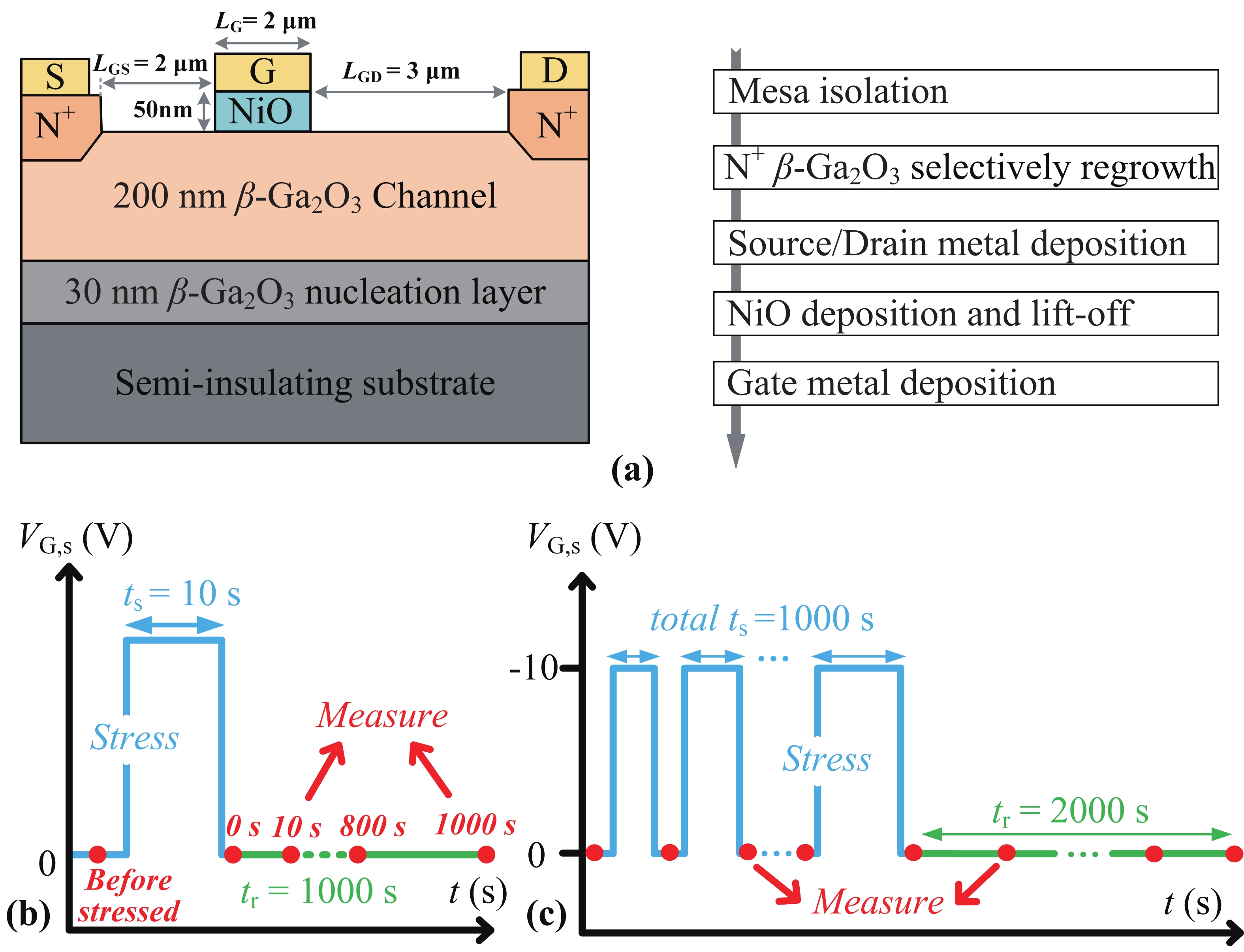
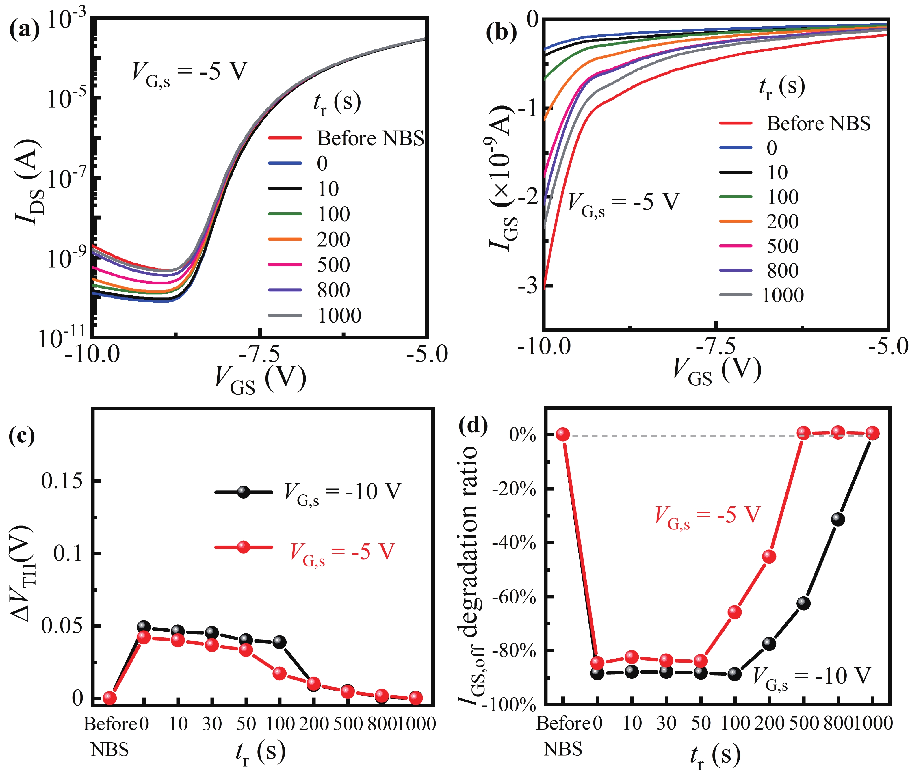
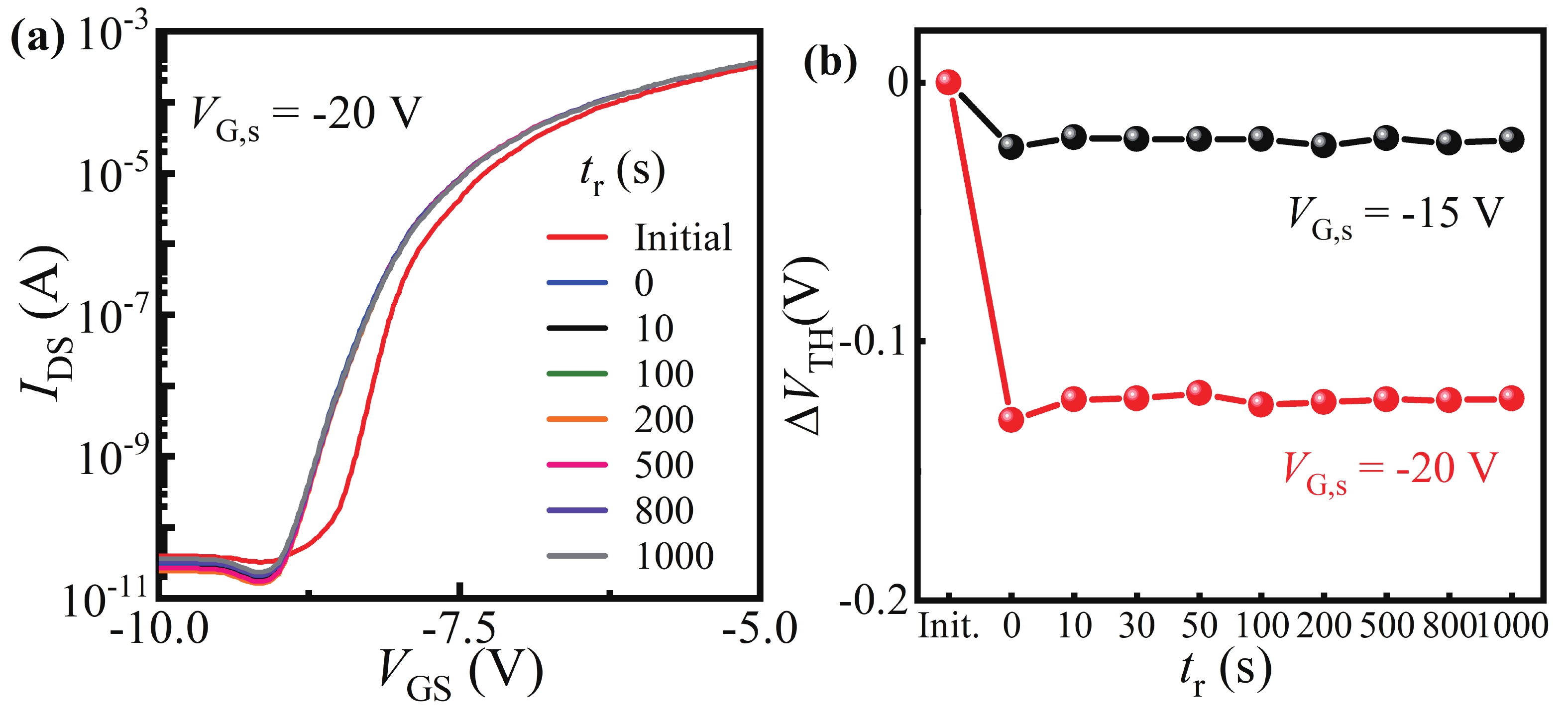
ARTICLES

Experimental investigation on the instability for NiO/β-Ga2O3 heterojunction-gate FETs under negative bias stress

Zhuolin Jiang1, Xiangnan Li1, Xuanze Zhou2, Yuxi Wei1, Jie Wei1, Guangwei Xu2, , Shibing Long2 and Xiaorong Luo1,

+ Author Affiliations

 Corresponding author: Guangwei Xu, xugw@ustc.edu.cn; Xiaorong Luo, xrluo@uestc.edu.cn

PDF

Turn off MathJax

Abstract: A NiO/β-Ga2O3 heterojunction-gate field effect transistor (HJ-FET) is fabricated and its instability mechanisms are experimentally investigated under different gate stress voltage (VG,s) and stress times (ts). Two different degradation mechanisms of the devices under negative bias stress (NBS) are identified. At low VG,s for a short ts, NiO bulk traps trapping/de-trapping electrons are responsible for decrease/recovery of the leakage current, respectively. At higher VG,s or long ts, the device transfer characteristic curves and threshold voltage (VTH) are almost permanently negatively shifted. This is because the interface dipoles are almost permanently ionized and neutralize the ionized charges in the space charge region (SCR) across the heterojunction interface, resulting in a narrowing SCR. This provides an important theoretical guide to study the reliability of NiO/β-Ga2O3 heterojunction devices in power electronic applications.

Key words: NiO/β-Ga2O3 heterojunctionFETNBSinstabilitybulk trapsinterface dipoles


[1]
Higashiwaki M, Sasaki K, Kuramata A, et al. Gallium oxide (Ga2O3) metal-semiconductor field-effect transistors on single-crystal β-Ga2O3 (010) substrates. Appl Phys Lett, 2012, 100, 013504 doi: doi.org/10.1063/1.3674287
[2]
Li W S, Nomoto K, Hu Z Y, et al. Field-plated Ga2O3 trench Schottky barrier diodes with a BV2/Ron, sp of up to 0.95 GW/cm2. IEEE Electron Device Lett, 2020, 41, 107 doi: 10.1109/LED.2019.2953559
[3]
Lv Y J, Liu H Y, Zhou X Y, et al. Lateral β-Ga2O3 MOSFETs with high power figure of merit of 277 MW/cm2. IEEE Electron Device Lett, 2020, 41, 537 doi: 10.1109/LED.2020.2974515
[4]
Wang C L, Zhou H, Zhang J C, et al. Hysteresis-free and μs-switching of D/E-modes Ga2O3 hetero-junction FETs with the BV2/Ron,sp of 0.74/0.28 GW/cm2. Appl Phys Lett, 2022, 120, 112101 doi: doi.org/10.1063/5.0084804
[5]
Gong H H, Zhou F, Xu W Z, et al. 1.37 kV/12 A NiO/β-Ga2O3 heterojunction diode with nanosecond reverse recovery and rugged surge-current capability. IEEE Trans Power Electron, 2021, 36, 12213 doi: 10.1109/TPEL.2021.3082640
[6]
Gong H H, Wang Z P, Yu X X, et al. Field-plated NiO/Ga2O3 p-n heterojunction power diodes with high-temperature thermal stability and near unity ideality factors. IEEE J Electron Devices Soc, 2021, 9, 1166 doi: 10.1109/JEDS.2021.3130305
[7]
Zhang J C, Dong P F, Dang K, et al. Ultra-wide bandgap semiconductor Ga2O3 power diodes. Nat Commun, 2022, 13, 3900 doi: 10.1038/s41467-022-31664-y
[8]
Wang Z P, Gong H H, Meng C X, et al. Majority and minority carrier traps in NiO/β-Ga2O3 p-n heterojunction diode. IEEE Trans Electron Devices, 2022, 69, 981 doi: 10.1109/TED.2022.3143491
[9]
Wang C L, Gong H H, Lei W N, et al. Demonstration of the p-NiO x/n-Ga2O3 heterojunction gate FETs and diodes with BV2/Ron, sp figures of merit of 0.39 GW/cm2 and 1.38 GW/cm2. IEEE Electron Device Lett, 2021, 42, 485 doi: 10.1109/LED.2021.3062851
[10]
Zhou X Z, Liu Q, Hao W B, et al. Normally-off β-Ga2O3 power heterojunction field-effect-transistor realized by p-NiO and recessed-gate. IEEE 34th International Symposium on Power Semiconductor Devices and ICs (ISPSD), 2022, 101 doi: 10.1109/ISPSD49238.2022.9813678
[11]
Jiang Z L, Wei J, Lv Y J, et al. Nonuniform mechanism for positive and negative bias stress instability in β-Ga2O3 MOSFET. IEEE Trans Electron Devices, 2022, 69, 5509 doi: 10.1109/TED.2022.3201825
[12]
Ye B, Gu Y, Xu H, et al. NBTI mitigation by optimized HKMG thermal processing in a FinFET technology. IEEE Trans Electron Devices, 2022, 69, 905 doi: 10.1109/TED.2021.3139566
[13]
Jiang Z L, Wei Y X, Lv Y J, et al. Experimental investigation on threshold voltage instability for β-Ga2O3 MOSFET under electrical and thermal stress. IEEE Trans Electron Devices, 2022, 69, 5048 doi: 10.1109/TED.2022.3188584
[14]
Guo A, del Alamo J A. Unified mechanism for positive-and negative-bias temperature instability in GaN MOSFETs. IEEE Trans Electron Devices, 2017, 64, 2142 doi: 10.1109/TED.2017.2686840
[15]
Zagni N, Cioni M, Chini A, et al. Mechanisms underlying the bidirectional VT shift after negative-bias temperature instability stress in carbon-doped fully recessed AlGaN/GaN MIS-HEMTs. IEEE Trans Electron Devices, 2021, 68, 2564 doi: 10.1109/TED.2021.3063664
[16]
Gong H H, Chen X H, Xu Y, et al. Band alignment and interface recombination in NiO/β-Ga2O3 type-II p-n heterojunctions. IEEE Trans Electron Devices, 2020, 67, 3341 doi: 10.1109/TED.2020.3001249
[17]
Donnelly J P, Milnes A G. The capacitance of p-n heterojunctions including the effects of interface states. IEEE Trans Electron Devices, 1967, 14, 63 doi: 10.1109/T-ED.1967.15900
[18]
Grundmann M, Karsthof R, von Wenckstern H. Interface recombination current in type II heterostructure bipolar diodes. ACS Appl Mater Interfaces, 2014, 6, 14785 doi: 10.1021/am504454g
Fig. 1.  (Color online) (a) Cross-sectional view of the proposed NiO/β-Ga2O3 HJ-FET and the main fabrication process flows. Schematic representation of the testing method for the analysis instability under NBS at (b) single pulse, and (c) multiple pulses with a prolonged ts.

Fig. 2.  (Color online) Measured DC characteristics: (a) log-scale transfer characteristics and (b) output characteristics.

Fig. 3.  (Color online) Measured (a) VGS-IDS and (b) VGS-IGS curves after NBS as a function of tr. Extracted (c) ∆VTH and (d) IGS, off degradation ratio.

Fig. 4.  (Color online) Measured (a) VGS-IDS and (b) VGS-IGS curves after NBS as a function of tr. Extracted (c) ∆VTH and (d) IGS, off degradation ratio.

Fig. 5.  (Color online) (a) Measured VGS-IDS curves during NBS at VG,s = -20 V. (b) Extracted ∆VTH.

Fig. 6.  (Color online) Schematic cross-sections of NiO/β-Ga2O3 HJ-FET (a) at initial, (b) under NBS, and (c) after NBS, respectively.

[1]
Higashiwaki M, Sasaki K, Kuramata A, et al. Gallium oxide (Ga2O3) metal-semiconductor field-effect transistors on single-crystal β-Ga2O3 (010) substrates. Appl Phys Lett, 2012, 100, 013504 doi: doi.org/10.1063/1.3674287
[2]
Li W S, Nomoto K, Hu Z Y, et al. Field-plated Ga2O3 trench Schottky barrier diodes with a BV2/Ron, sp of up to 0.95 GW/cm2. IEEE Electron Device Lett, 2020, 41, 107 doi: 10.1109/LED.2019.2953559
[3]
Lv Y J, Liu H Y, Zhou X Y, et al. Lateral β-Ga2O3 MOSFETs with high power figure of merit of 277 MW/cm2. IEEE Electron Device Lett, 2020, 41, 537 doi: 10.1109/LED.2020.2974515
[4]
Wang C L, Zhou H, Zhang J C, et al. Hysteresis-free and μs-switching of D/E-modes Ga2O3 hetero-junction FETs with the BV2/Ron,sp of 0.74/0.28 GW/cm2. Appl Phys Lett, 2022, 120, 112101 doi: doi.org/10.1063/5.0084804
[5]
Gong H H, Zhou F, Xu W Z, et al. 1.37 kV/12 A NiO/β-Ga2O3 heterojunction diode with nanosecond reverse recovery and rugged surge-current capability. IEEE Trans Power Electron, 2021, 36, 12213 doi: 10.1109/TPEL.2021.3082640
[6]
Gong H H, Wang Z P, Yu X X, et al. Field-plated NiO/Ga2O3 p-n heterojunction power diodes with high-temperature thermal stability and near unity ideality factors. IEEE J Electron Devices Soc, 2021, 9, 1166 doi: 10.1109/JEDS.2021.3130305
[7]
Zhang J C, Dong P F, Dang K, et al. Ultra-wide bandgap semiconductor Ga2O3 power diodes. Nat Commun, 2022, 13, 3900 doi: 10.1038/s41467-022-31664-y
[8]
Wang Z P, Gong H H, Meng C X, et al. Majority and minority carrier traps in NiO/β-Ga2O3 p-n heterojunction diode. IEEE Trans Electron Devices, 2022, 69, 981 doi: 10.1109/TED.2022.3143491
[9]
Wang C L, Gong H H, Lei W N, et al. Demonstration of the p-NiO x/n-Ga2O3 heterojunction gate FETs and diodes with BV2/Ron, sp figures of merit of 0.39 GW/cm2 and 1.38 GW/cm2. IEEE Electron Device Lett, 2021, 42, 485 doi: 10.1109/LED.2021.3062851
[10]
Zhou X Z, Liu Q, Hao W B, et al. Normally-off β-Ga2O3 power heterojunction field-effect-transistor realized by p-NiO and recessed-gate. IEEE 34th International Symposium on Power Semiconductor Devices and ICs (ISPSD), 2022, 101 doi: 10.1109/ISPSD49238.2022.9813678
[11]
Jiang Z L, Wei J, Lv Y J, et al. Nonuniform mechanism for positive and negative bias stress instability in β-Ga2O3 MOSFET. IEEE Trans Electron Devices, 2022, 69, 5509 doi: 10.1109/TED.2022.3201825
[12]
Ye B, Gu Y, Xu H, et al. NBTI mitigation by optimized HKMG thermal processing in a FinFET technology. IEEE Trans Electron Devices, 2022, 69, 905 doi: 10.1109/TED.2021.3139566
[13]
Jiang Z L, Wei Y X, Lv Y J, et al. Experimental investigation on threshold voltage instability for β-Ga2O3 MOSFET under electrical and thermal stress. IEEE Trans Electron Devices, 2022, 69, 5048 doi: 10.1109/TED.2022.3188584
[14]
Guo A, del Alamo J A. Unified mechanism for positive-and negative-bias temperature instability in GaN MOSFETs. IEEE Trans Electron Devices, 2017, 64, 2142 doi: 10.1109/TED.2017.2686840
[15]
Zagni N, Cioni M, Chini A, et al. Mechanisms underlying the bidirectional VT shift after negative-bias temperature instability stress in carbon-doped fully recessed AlGaN/GaN MIS-HEMTs. IEEE Trans Electron Devices, 2021, 68, 2564 doi: 10.1109/TED.2021.3063664
[16]
Gong H H, Chen X H, Xu Y, et al. Band alignment and interface recombination in NiO/β-Ga2O3 type-II p-n heterojunctions. IEEE Trans Electron Devices, 2020, 67, 3341 doi: 10.1109/TED.2020.3001249
[17]
Donnelly J P, Milnes A G. The capacitance of p-n heterojunctions including the effects of interface states. IEEE Trans Electron Devices, 1967, 14, 63 doi: 10.1109/T-ED.1967.15900
[18]
Grundmann M, Karsthof R, von Wenckstern H. Interface recombination current in type II heterostructure bipolar diodes. ACS Appl Mater Interfaces, 2014, 6, 14785 doi: 10.1021/am504454g
  • Search

    Advanced Search >>

    GET CITATION

    shu

    Export: BibTex EndNote

    Article Metrics

    Article views: 997 Times PDF downloads: 165 Times Cited by: 0 Times

    History

    Received: 30 January 2023 Revised: 17 March 2023 Online: Accepted Manuscript: 10 May 2023Uncorrected proof: 05 June 2023Corrected proof: 26 June 2023Published: 10 July 2023

    Catalog

      Email This Article

      User name:
      Email:*请输入正确邮箱
      Code:*验证码错误
      Zhuolin Jiang, Xiangnan Li, Xuanze Zhou, Yuxi Wei, Jie Wei, Guangwei Xu, Shibing Long, Xiaorong Luo. Experimental investigation on the instability for NiO/β-Ga2O3 heterojunction-gate FETs under negative bias stress[J]. Journal of Semiconductors, 2023, 44(7): 072803. doi: 10.1088/1674-4926/44/7/072803 Z L Jiang, X N Li, X Z Zhou, Y X Wei, J Wei, G W Xu, S B Long, X R Luo. Experimental investigation on the instability for NiO/β-Ga2O3 heterojunction-gate FETs under negative bias stress[J]. J. Semicond, 2023, 44(7): 072803. doi: 10.1088/1674-4926/44/7/072803Export: BibTex EndNote
      Citation:
      Zhuolin Jiang, Xiangnan Li, Xuanze Zhou, Yuxi Wei, Jie Wei, Guangwei Xu, Shibing Long, Xiaorong Luo. Experimental investigation on the instability for NiO/β-Ga2O3 heterojunction-gate FETs under negative bias stress[J]. Journal of Semiconductors, 2023, 44(7): 072803. doi: 10.1088/1674-4926/44/7/072803

      Z L Jiang, X N Li, X Z Zhou, Y X Wei, J Wei, G W Xu, S B Long, X R Luo. Experimental investigation on the instability for NiO/β-Ga2O3 heterojunction-gate FETs under negative bias stress[J]. J. Semicond, 2023, 44(7): 072803. doi: 10.1088/1674-4926/44/7/072803
      Export: BibTex EndNote

      Experimental investigation on the instability for NiO/β-Ga2O3 heterojunction-gate FETs under negative bias stress

      doi: 10.1088/1674-4926/44/7/072803
      More Information
      • Author Bio:

        Zhuolin Jiang received the M.S. degree from the University of Electronic Science and Technology of China (UESTC), Chengdu, China, in 2017. He was a senior researcher with the BOE Technology Group Co., Ltd in 2020. He is currently pursuing the Ph.D. degree in microelectronics with the University of Electronic Science and Technology of China, Chengdu, China

        Guangwei Xu received his Ph.D. degree at IMECAS in 2017. Then, he joined the University of California, Los Angeles as a postdoc. He joined the University of Science and Technology of China as an associate research fellow in Shibing Long Group in 2019. His research focuses on wide bandgap semiconductor power device fabrication, device defect state measurement and device modeling

        Xiaorong Luo received the Ph.D. degree in microelectronics from the University of Electronic Science and Technology of China (UESTC), Chengdu, China, in 2007. She is currently the Vice Director of the Department of Microelectronics Science and Engineering with UESTC

      • Corresponding author: xugw@ustc.edu.cnxrluo@uestc.edu.cn
      • Received Date: 2023-01-30
      • Revised Date: 2023-03-17
      • Available Online: 2023-05-10

      Catalog

        /

        DownLoad:  Full-Size Img  PowerPoint
        Return
        Return