


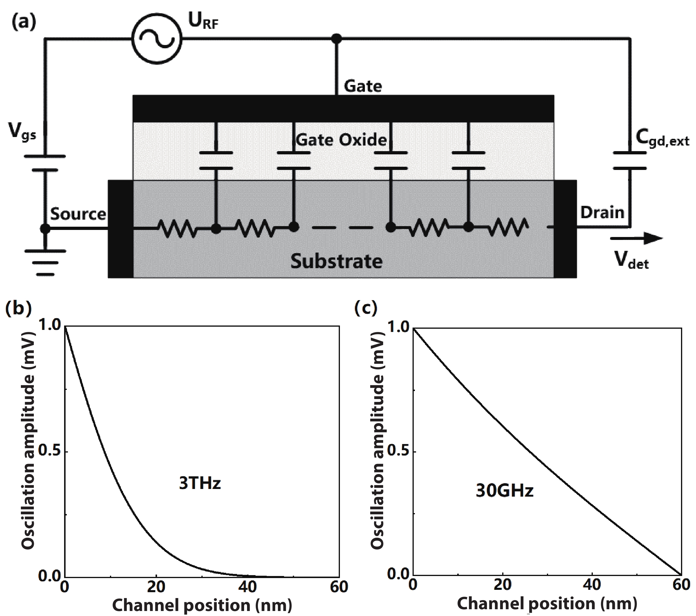
Fig. 1.
(a) NQS RC-ladder model, (b) spatial evolution of carrier oscillation amplitude at excitation of 3.0 THz and (c) spatial evolution of carrier oscillation amplitude at excitation of 30 GHz.
ARTICLES
Min Liu1, 2, Ziteng Cai1, 3, Jian Liu1, 2, Nanjian Wu1, 2 and Liyuan Liu1, 2,
Corresponding author: Liyuan Liu, liuly@semi.ac.cn
Abstract: This paper describes a promising route for the exploration and development of 3.0 THz sensing and imaging with FET-based power detectors in a standard 65 nm CMOS process. Based on the plasma-wave theory proposed by Dyakonov and Shur, we designed high-responsivity and low-noise multiple detectors for monitoring a pulse-mode 3.0 THz quantum cascade laser (QCL). Furthermore, we present a fully integrated high-speed 32 × 32-pixel 3.0 THz CMOS image sensor (CIS). The full CIS measures 2.81 × 5.39 mm2 and achieves a 423 V/W responsivity (Rv) and a 5.3 nW integral noise equivalent power (NEP) at room temperature. In experiments, we demonstrate a testing speed reaching 319 fps under continuous-wave (CW) illumination of a 3.0 THz QCL. The results indicate that our terahertz CIS has excellent potential in cost-effective and commercial THz imaging and material detection.
Key words: power detectors, quantum cascade laser (QCL), CMOS image sensor (CIS), terahertz
| [1] |
Su Y R, Ma W B, Yang Y M. Perovskite semiconductors for direct X-ray detection and imaging. J Semicond, 2020, 41, 051204 doi: 10.1088/1674-4926/41/5/051204
|
| [2] |
Sun Q S, He Y Z, Liu K, et al. Recent advances in terahertz technology for biomedical applications. Quant Imaging Med Surg, 2017, 7, 345 doi: 10.21037/qims.2017.06.02
|
| [3] |
Son J H, Oh S J, Cheon H. Potential clinical applications of terahertz radiation. J Appl Phys, 2019, 125, 190901 doi: 10.1063/1.5080205
|
| [4] |
D’Arco A, Di Di Fabrizio M, Dolci V, et al. THz pulsed imaging in biomedical applications. Condens Matter, 2020, 5, 25 doi: 10.3390/condmat5020025
|
| [5] |
Woolard D L, Jensen J O, Hwu R J, et al. Terahertz science and technology for military and security applications. World scinetific, 2007
|
| [6] |
Brun M A, Formanek F, Yasuda A, et al. Terahertz imaging applied to cancer diagnosis. Phys Med Biol, 2010, 55, 4615 doi: 10.1088/0031-9155/55/16/001
|
| [7] |
Zhang H, Sfarra S, Saluja K, et al. Non-destructive investigation of paintings on canvas by continuous wave terahertz imaging and flash thermography. J Nondestruct Eval, 2017, 36, 34 doi: 10.1007/s10921-017-0414-8
|
| [8] |
Kawase K, Shibuya T, Hayashi S, et al. THz imaging techniques for nondestructive inspections. Comptes Rendus Physique, 2010, 11, 510 doi: 10.1016/j.crhy.2010.04.003
|
| [9] |
Steyaert W, Reynaert P. A THz signal source with integrated antenna for non-destructive testing in 28nm bulk CMOS. 2015 IEEE Asian Solid-State Circuits Conference (A-SSCC), 2016, 1 doi: 10.1109/ASSCC.2015.7387436
|
| [10] |
Dyakonov M, Shur M. Shallow water analogy for a ballistic field effect transistor: New mechanism of plasma wave generation by dc current. Phys Rev Lett, 1993, 71, 2465 doi: 10.1103/PhysRevLett.71.2465
|
| [11] |
Ojefors E, Pfeiffer U R, Lisauskas A, et al. A 0.65 THz focal-plane array in a quarter-micron CMOS process technology. IEEE J Solid State Circuits, 2009, 44, 1968 doi: 10.1109/JSSC.2009.2021911
|
| [12] |
Al Hadi R, Sherry H, Grzyb J, et al. A 1 k-pixel video camera for 0.7–1.1 terahertz imaging applications in 65-nm CMOS. IEEE J Solid State Circuits, 2012, 47, 2999 doi: 10.1109/JSSC.2012.2217851
|
| [13] |
Kim D Y, Park S, Han R, et al. 820-GHz imaging array using diode-connected NMOS transistors in 130-nm CMOS. 2013 Symposium on VLSI Circuits, Kyoto, Japan, 2013, C12
|
| [14] |
Lisauskas A, Bauer M, Boppel S, et al. Exploration of terahertz imaging with silicon MOSFETs. J Infrared Milli Terahz Waves, 2014, 35, 63 doi: 10.1007/s10762-013-0047-7
|
| [15] |
Fang T, Dou R J, Liu L Y, et al. A 25 fps 32 × 24 digital CMOS terahertz image sensor. 2018 IEEE Asian Solid-State Circuits Conference (A-SSCC), 2018, 87 doi: 10.1109/ASSCC.2018.8579336
|
| [16] |
Yokoyama S, Ikebe M, Kanazawa Y, et al. 5.8 A 32 × 32-pixel 0.9THz imager with pixel-parallel 12b VCO-based ADC in 0.18μm CMOS. 2019 IEEE International Solid-State Circuits Conference-(ISSCC), 2019, 108 doi: 10.1109/ISSCC.2019.8662483
|
| [17] |
Jain R, Hillger P, Grzyb J, et al. 34.3 A 32 × 32 pixel 0.46-to-0.75THz light-field camera SoC in 0.13μm CMOS. 2021 IEEE International Solid- State Circuits Conference (ISSCC), 2021, 484 doi: 10.1109/ISSCC42613.2021.9365832
|
| [18] |
Zhuo N, Liu F Q, Wang Z G. Quantum cascade lasers: From sketch to mainstream in the mid and far infrared. J Semicond, 2020, 41, 010301 doi: 10.1088/1674-4926/41/1/010301
|
| [19] |
Kindness S J, Jessop D S, Wei B, et al. 100% amplitude modulation of an external cavity terahertz QCL using an optoelectronic chopper based on metamaterials and graphene. 2017 Conference on Lasers and Electro-Optics Europe & European Quantum Electronics Conference (CLEO/Europe-EQEC), 2017, 1 doi: 10.1109/CLEOE-EQEC.2017.8086346
|
| [20] |
Jin Y, Reno J L, Kumar S. Phase-locked terahertz plasmonic laser array with 2 W output power in a single spectral mode. Optica, OPTICA, 2020, 7, 708 doi: 10.1364/OPTICA.390852
|
| [21] |
Li W J, Ma Y, Xu Y F, et al. Continuous-wave single-mode quantum cascade laser at 5.1 THz based on graded sampled grating design. Photon Res, 2022, 10, 2686 doi: 10.1364/PRJ.467974
|
| [22] |
International Telecommunication Union ITU-R P. 676-11: Attenuation by Atmospheric Gases (ITU, 2016).
|
| [23] |
The HITRAN Database. Accessed on Mar. 2019. [Online]. Available: http://www.cfa.harvard.edu/hitran/
|
| [24] |
Fang T, Liu Z Y, Liu L Y, et al. Detection of 3.0 THz wave with a detector in 65 nm standard CMOS process. 2017 IEEE Asian Solid-State Circuits Conference (A-SSCC), 2017, 189 doi: 10.11972/j.issn.1001-9014.2020.01.009
|
| [25] |
Fang T, Liu L Y, Liu Z Y, et al. A 3.0 THz detector in 65 nm standard CMOS process. J Infrared Millim Waves, 2020, 39, 56 doi: 10.1109/ASSCC.2017.8240248
|
| [26] |
Ikamas K, Lisauskas A, Boppel S, et al. Efficient detection of 3 THz radiation from quantum cascade laser using silicon CMOS detectors. J Infrared Millim Terahertz Waves, 2017, 38, 1183 doi: 10.1007/s10762-017-0407-9
|
| [27] |
Boppel S, Lisauskas A, Mundt M, et al. CMOS integrated antenna-coupled field-effect transistors for the detection of radiation from 0.2 to 4.3 THz. IEEE Trans Microw Theory Tech, 2012, 60, 3834 doi: 10.1109/TMTT.2012.2221732
|
| [28] |
Smith T J, Broome A, Stanley D, et al. A hybrid THz imaging system with a 100-pixel CMOS imager and a 3.25–3.50 THz quantum cascade laser frequency comb. ESSCIRC 2019-IEEE 45th European Solid State Circuits Conference (ESSCIRC), 2019, 151 doi: 10.1109/ESSCIRC.2019.8902823
|
| [29] |
Liu Z Y, Liu L Y, Yang J, et al. A CMOS fully integrated 860-GHz terahertz sensor. IEEE Trans Terahertz Sci Technol, 2017, 7, 455 doi: 10.1109/TTHZ.2017.2692040
|
| [30] |
Knap W, Teppe F, Meziani Y, et al. Plasma wave detection of sub-terahertz and terahertz radiation by silicon field-effect transistors. Appl Phys Lett, 2004, 85, 675 doi: 10.1063/1.1775034
|
| [31] |
Dyakonov M, Shur M. Detection, mixing, and frequency multiplication of terahertz radiation by two-dimensional electronic fluid. IEEE Trans Electron Devices, 1996, 43, 380 doi: 10.1109/16.485650
|
| [32] |
Crowne F J. Microwave response of a high electron mobility transistor in the presence of a Dyakonov–Shur instability. J Appl Phys, 2002, 91, 5377 doi: 10.1063/1.1448891
|
| [33] |
Lisauskas A, Glaab D, Roskos H G, et al. Terahertz imaging with Si MOSFET focal-plane arrays. SPIE OPTO: Integrated Optoelectronic Devices. Proc SPIE 7215, Terahertz Technology and Applications II, 2009, 119 doi: 10.1117/12.809552
|
| [34] |
THORLABS ITC4000 Series Operation Manual, Version 3.9. New Jersey, U. S. A: Thorlabs, Inc. , Jul. 2018.
|
| [35] |
Guo Z J, Yu N M, Wu L S. Column readout circuit with improved offset mismatch and charge sharing for CMOS image sensor. J Semicond, 2019, 40, 122404 doi: 10.1088/1674-4926/40/12/122404
|
| [36] |
Wu R, Huijsing J H, Makinwa K A A. Read-out integrated circuits. Springer, 2012, 137
|
| [37] |
Fang T, Liu M, Liu L Y, et al. A 32 × 32 array terahertz sensor in 65-nm CMOS technology. 2021 IEEE International Conference on Integrated Circuits, Technologies and Applications (ICTA), 2022, 259j doi: 10.1109/ICTA53157.2021.9661999
|
| [38] |
Javadi E, But D B, Ikamas K, et al. Sensitivity of field-effect transistor-based terahertz detectors. Sensors, 2021, 21, 2909 doi: 10.3390/s21092909
|
| [39] |
Ferreras M, Čibiraitė-Lukenskienė D, Lisauskas A, et al. Broadband sensing around 1 THz via a novel biquad-antenna-coupled low-NEP detector in CMOS. IEEE Trans Terahertz Sci Technol, 2021, 11, 16 doi: 10.1109/TTHZ.2020.3031483
|
| [40] |
Zdanevičius J, Bauer M, Boppel S, et al. Camera for high-speed THz imaging. J Infrared Milli Terahz Waves, 2015, 36, 986 doi: 10.1007/s10762-015-0169-1
|
| [41] |
Boukhayma A, Dupret A, Rostaing J P, et al. A low-noise CMOS THz imager based on source modulation and an In-pixel high-Q passive switched-capacitor N-path filter. Sensors (Basel), 2016, 16, 325 doi: 10.3390/s16030325
|
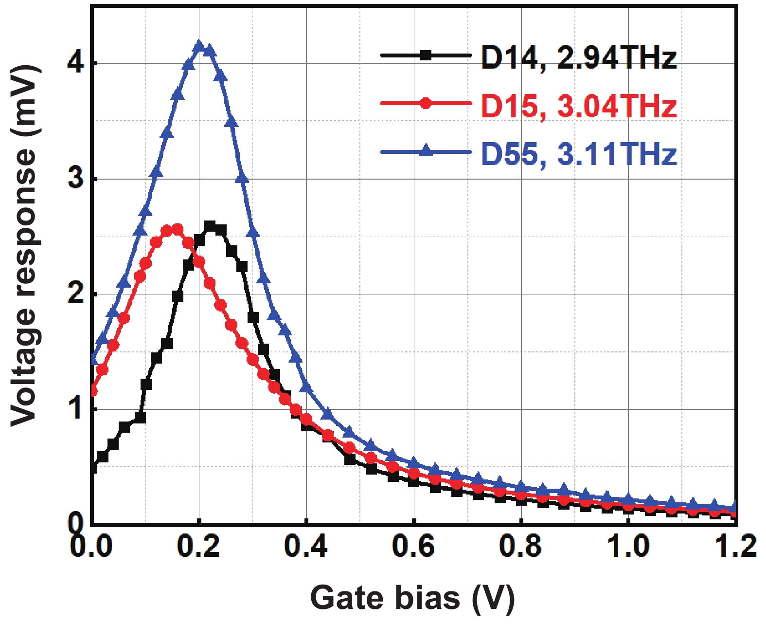


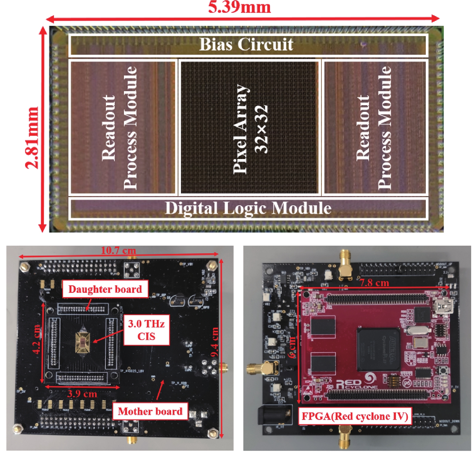

Table 1. Parameters and measured results of partial FET-based detectors.
| Detector1 | Patch size (µm2) | TL1 (µm2) | Resonant frequency (THz) | Directivity (dBi) | Max. voltage response (mV) | Responsivity2 (V/W) | NEP (pW/Hz1/2) | SNR (dB) |
| D88 | 30 × 8 | 4.2 × 2 | 2.80 | 3.50 | 2.72@0.79 V | 422 | 189 | 90 |
| D13 | 30 × 2 | 6.0 × 2 | 2.85 | 3.11 | 2.13@0.27 V | 374 | 56 | 100 |
| D95 | 30 × 7 | 4.5 × 2 | 2.89 | 3.12 | 2.93@0.19 V | 528 | 174 | 90 |
| D14 | 30 × 2 | 5.5 × 2 | 2.94 | 2.75 | 2.59@0.23 V | 526 | 123 | 92 |
| D15 | 30 × 2 | 5.0 × 2 | 3.04 | 2.29 | 2.56@0.16 V | 618 | 139 | 89 |
| D72 | 30 × 4 | 4.5 × 2 | 3.04 | 2.37 | 3.35@0.16 V | 791 | 245 | 84 |
| D55 | 20 × 2 | 6.0 × 2 | 3.11 | 3.79 | 4.15@0.21 V | 741 | 174 | 90 |
| D36 | 25 × 2 | 5.0 × 2 | 3.16 | 2.22 | 3.22@0.13 V | 855 | 71 | 94 |
| D16 | 30 × 2 | 4.0 × 2 | 3.25 | 1.88 | 3.02@0.18 V | 915 | 39 | 98 |
| 1 Dxy refers to the detector in the x-th row and y-th column. | ||||||||
| 2 The responsivity is estimated according to the raster-scanning source beam with D14. | ||||||||
 DownLoad: CSV
Table 2. Comparison with other published CMOS imagers.
| Freq. (THz) | Technology | Pixel (x×y) | Rv1 (kV/W) | NEP (nW) | Readout chain | Frame rate (fps) | Optics | Reference |
| 3.0 | 65-nm CMOS | 32 × 32 | 423 | 5.4 | On-chip | Max.319 | None | This work |
| 0.79−0.96 | 65-nm CMOS | 32 × 32 | 562−1124 | 10−20 | External | Max.500 | Si lens | [12] |
| 0.59 | 150-nm CMOS | 12 × 12 | 348 | 15.2 | External | 16 | None | [14] |
| 0.46−0.75 | 130-nm CMOS | 32 × 32 | 0.014 A/W | 36 | On-chip | 25 | Si lens | [17] |
| 0.27−0.6 | 130-nm CMOS | 31 × 31 | 272−378 | 0.6−0.8 | On-chip | 25−100 | None | [41] |
| 1 The responsivity is a normalized value excluding gain and measured at video mode. | ||||||||
DownLoad: CSV
| [1] |
Su Y R, Ma W B, Yang Y M. Perovskite semiconductors for direct X-ray detection and imaging. J Semicond, 2020, 41, 051204 doi: 10.1088/1674-4926/41/5/051204
|
| [2] |
Sun Q S, He Y Z, Liu K, et al. Recent advances in terahertz technology for biomedical applications. Quant Imaging Med Surg, 2017, 7, 345 doi: 10.21037/qims.2017.06.02
|
| [3] |
Son J H, Oh S J, Cheon H. Potential clinical applications of terahertz radiation. J Appl Phys, 2019, 125, 190901 doi: 10.1063/1.5080205
|
| [4] |
D’Arco A, Di Di Fabrizio M, Dolci V, et al. THz pulsed imaging in biomedical applications. Condens Matter, 2020, 5, 25 doi: 10.3390/condmat5020025
|
| [5] |
Woolard D L, Jensen J O, Hwu R J, et al. Terahertz science and technology for military and security applications. World scinetific, 2007
|
| [6] |
Brun M A, Formanek F, Yasuda A, et al. Terahertz imaging applied to cancer diagnosis. Phys Med Biol, 2010, 55, 4615 doi: 10.1088/0031-9155/55/16/001
|
| [7] |
Zhang H, Sfarra S, Saluja K, et al. Non-destructive investigation of paintings on canvas by continuous wave terahertz imaging and flash thermography. J Nondestruct Eval, 2017, 36, 34 doi: 10.1007/s10921-017-0414-8
|
| [8] |
Kawase K, Shibuya T, Hayashi S, et al. THz imaging techniques for nondestructive inspections. Comptes Rendus Physique, 2010, 11, 510 doi: 10.1016/j.crhy.2010.04.003
|
| [9] |
Steyaert W, Reynaert P. A THz signal source with integrated antenna for non-destructive testing in 28nm bulk CMOS. 2015 IEEE Asian Solid-State Circuits Conference (A-SSCC), 2016, 1 doi: 10.1109/ASSCC.2015.7387436
|
| [10] |
Dyakonov M, Shur M. Shallow water analogy for a ballistic field effect transistor: New mechanism of plasma wave generation by dc current. Phys Rev Lett, 1993, 71, 2465 doi: 10.1103/PhysRevLett.71.2465
|
| [11] |
Ojefors E, Pfeiffer U R, Lisauskas A, et al. A 0.65 THz focal-plane array in a quarter-micron CMOS process technology. IEEE J Solid State Circuits, 2009, 44, 1968 doi: 10.1109/JSSC.2009.2021911
|
| [12] |
Al Hadi R, Sherry H, Grzyb J, et al. A 1 k-pixel video camera for 0.7–1.1 terahertz imaging applications in 65-nm CMOS. IEEE J Solid State Circuits, 2012, 47, 2999 doi: 10.1109/JSSC.2012.2217851
|
| [13] |
Kim D Y, Park S, Han R, et al. 820-GHz imaging array using diode-connected NMOS transistors in 130-nm CMOS. 2013 Symposium on VLSI Circuits, Kyoto, Japan, 2013, C12
|
| [14] |
Lisauskas A, Bauer M, Boppel S, et al. Exploration of terahertz imaging with silicon MOSFETs. J Infrared Milli Terahz Waves, 2014, 35, 63 doi: 10.1007/s10762-013-0047-7
|
| [15] |
Fang T, Dou R J, Liu L Y, et al. A 25 fps 32 × 24 digital CMOS terahertz image sensor. 2018 IEEE Asian Solid-State Circuits Conference (A-SSCC), 2018, 87 doi: 10.1109/ASSCC.2018.8579336
|
| [16] |
Yokoyama S, Ikebe M, Kanazawa Y, et al. 5.8 A 32 × 32-pixel 0.9THz imager with pixel-parallel 12b VCO-based ADC in 0.18μm CMOS. 2019 IEEE International Solid-State Circuits Conference-(ISSCC), 2019, 108 doi: 10.1109/ISSCC.2019.8662483
|
| [17] |
Jain R, Hillger P, Grzyb J, et al. 34.3 A 32 × 32 pixel 0.46-to-0.75THz light-field camera SoC in 0.13μm CMOS. 2021 IEEE International Solid- State Circuits Conference (ISSCC), 2021, 484 doi: 10.1109/ISSCC42613.2021.9365832
|
| [18] |
Zhuo N, Liu F Q, Wang Z G. Quantum cascade lasers: From sketch to mainstream in the mid and far infrared. J Semicond, 2020, 41, 010301 doi: 10.1088/1674-4926/41/1/010301
|
| [19] |
Kindness S J, Jessop D S, Wei B, et al. 100% amplitude modulation of an external cavity terahertz QCL using an optoelectronic chopper based on metamaterials and graphene. 2017 Conference on Lasers and Electro-Optics Europe & European Quantum Electronics Conference (CLEO/Europe-EQEC), 2017, 1 doi: 10.1109/CLEOE-EQEC.2017.8086346
|
| [20] |
Jin Y, Reno J L, Kumar S. Phase-locked terahertz plasmonic laser array with 2 W output power in a single spectral mode. Optica, OPTICA, 2020, 7, 708 doi: 10.1364/OPTICA.390852
|
| [21] |
Li W J, Ma Y, Xu Y F, et al. Continuous-wave single-mode quantum cascade laser at 5.1 THz based on graded sampled grating design. Photon Res, 2022, 10, 2686 doi: 10.1364/PRJ.467974
|
| [22] |
International Telecommunication Union ITU-R P. 676-11: Attenuation by Atmospheric Gases (ITU, 2016).
|
| [23] |
The HITRAN Database. Accessed on Mar. 2019. [Online]. Available: http://www.cfa.harvard.edu/hitran/
|
| [24] |
Fang T, Liu Z Y, Liu L Y, et al. Detection of 3.0 THz wave with a detector in 65 nm standard CMOS process. 2017 IEEE Asian Solid-State Circuits Conference (A-SSCC), 2017, 189 doi: 10.11972/j.issn.1001-9014.2020.01.009
|
| [25] |
Fang T, Liu L Y, Liu Z Y, et al. A 3.0 THz detector in 65 nm standard CMOS process. J Infrared Millim Waves, 2020, 39, 56 doi: 10.1109/ASSCC.2017.8240248
|
| [26] |
Ikamas K, Lisauskas A, Boppel S, et al. Efficient detection of 3 THz radiation from quantum cascade laser using silicon CMOS detectors. J Infrared Millim Terahertz Waves, 2017, 38, 1183 doi: 10.1007/s10762-017-0407-9
|
| [27] |
Boppel S, Lisauskas A, Mundt M, et al. CMOS integrated antenna-coupled field-effect transistors for the detection of radiation from 0.2 to 4.3 THz. IEEE Trans Microw Theory Tech, 2012, 60, 3834 doi: 10.1109/TMTT.2012.2221732
|
| [28] |
Smith T J, Broome A, Stanley D, et al. A hybrid THz imaging system with a 100-pixel CMOS imager and a 3.25–3.50 THz quantum cascade laser frequency comb. ESSCIRC 2019-IEEE 45th European Solid State Circuits Conference (ESSCIRC), 2019, 151 doi: 10.1109/ESSCIRC.2019.8902823
|
| [29] |
Liu Z Y, Liu L Y, Yang J, et al. A CMOS fully integrated 860-GHz terahertz sensor. IEEE Trans Terahertz Sci Technol, 2017, 7, 455 doi: 10.1109/TTHZ.2017.2692040
|
| [30] |
Knap W, Teppe F, Meziani Y, et al. Plasma wave detection of sub-terahertz and terahertz radiation by silicon field-effect transistors. Appl Phys Lett, 2004, 85, 675 doi: 10.1063/1.1775034
|
| [31] |
Dyakonov M, Shur M. Detection, mixing, and frequency multiplication of terahertz radiation by two-dimensional electronic fluid. IEEE Trans Electron Devices, 1996, 43, 380 doi: 10.1109/16.485650
|
| [32] |
Crowne F J. Microwave response of a high electron mobility transistor in the presence of a Dyakonov–Shur instability. J Appl Phys, 2002, 91, 5377 doi: 10.1063/1.1448891
|
| [33] |
Lisauskas A, Glaab D, Roskos H G, et al. Terahertz imaging with Si MOSFET focal-plane arrays. SPIE OPTO: Integrated Optoelectronic Devices. Proc SPIE 7215, Terahertz Technology and Applications II, 2009, 119 doi: 10.1117/12.809552
|
| [34] |
THORLABS ITC4000 Series Operation Manual, Version 3.9. New Jersey, U. S. A: Thorlabs, Inc. , Jul. 2018.
|
| [35] |
Guo Z J, Yu N M, Wu L S. Column readout circuit with improved offset mismatch and charge sharing for CMOS image sensor. J Semicond, 2019, 40, 122404 doi: 10.1088/1674-4926/40/12/122404
|
| [36] |
Wu R, Huijsing J H, Makinwa K A A. Read-out integrated circuits. Springer, 2012, 137
|
| [37] |
Fang T, Liu M, Liu L Y, et al. A 32 × 32 array terahertz sensor in 65-nm CMOS technology. 2021 IEEE International Conference on Integrated Circuits, Technologies and Applications (ICTA), 2022, 259j doi: 10.1109/ICTA53157.2021.9661999
|
| [38] |
Javadi E, But D B, Ikamas K, et al. Sensitivity of field-effect transistor-based terahertz detectors. Sensors, 2021, 21, 2909 doi: 10.3390/s21092909
|
| [39] |
Ferreras M, Čibiraitė-Lukenskienė D, Lisauskas A, et al. Broadband sensing around 1 THz via a novel biquad-antenna-coupled low-NEP detector in CMOS. IEEE Trans Terahertz Sci Technol, 2021, 11, 16 doi: 10.1109/TTHZ.2020.3031483
|
| [40] |
Zdanevičius J, Bauer M, Boppel S, et al. Camera for high-speed THz imaging. J Infrared Milli Terahz Waves, 2015, 36, 986 doi: 10.1007/s10762-015-0169-1
|
| [41] |
Boukhayma A, Dupret A, Rostaing J P, et al. A low-noise CMOS THz imager based on source modulation and an In-pixel high-Q passive switched-capacitor N-path filter. Sensors (Basel), 2016, 16, 325 doi: 10.3390/s16030325
|


Article views: 1046 Times PDF downloads: 151 Times Cited by: 0 Times
Received: 24 January 2023 Revised: 23 March 2023 Online: Accepted Manuscript: 26 May 2023Uncorrected proof: 31 August 2023Corrected proof: 04 September 2023Published: 10 October 2023
| Citation: |
Min Liu, Ziteng Cai, Jian Liu, Nanjian Wu, Liyuan Liu. Exploration of high-speed 3.0 THz imaging with a 65 nm CMOS process[J]. Journal of Semiconductors, 2023, 44(10): 102401. doi: 10.1088/1674-4926/44/10/102401
****
M Liu, Z T Cai, J Liu, N J Wu, L Y Liu. Exploration of high-speed 3.0 THz imaging with a 65 nm CMOS process[J]. J. Semicond, 2023, 44(10): 102401. doi: 10.1088/1674-4926/44/10/102401

|
 Min Liu:(S’22) is pursuing a Ph.D. degree with the State Key Laboratory of Super-lattices and Microstructures, Institute of Semiconductors, Chinese Academy of Sciences, Beijing, China. Her research interests include low-noise readout integrated circuits design, terahertz spectrometer design, and CMOS-integrated terahertz image sensors design
 Ziteng Cai:(S’22) is pursuing a B.S. degree at the Beijing University of Technology, Beijing, China, and trained at the State Key Laboratory of Super-lattices and Microstructures, Institute of Semiconductors, Chinese Academy of Sciences, Beijing, China. His research interests include terahertz detector design and CMOS-integrated terahertz image sensor design
 Jian Liu:is a Full Professor in microelectronics and solid-state electronics with the State Key Laboratory of Super-lattices and Microstructures, Institute of Semiconductors, Chinese Academy of Sciences, Beijing, China, since 2005. His research interests include semiconductor optoelectronic detectors, terahertz imagers, and metamaterials
 Nanjian Wu:(M’06) has been a Professor with the State Key Laboratory of Super-lattices and Microstructures, Institute of Semiconductors, Chinese Academy of Sciences, Beijing, China, since 2000. Since 2009, he has been an Honorable Guest Professor with the Research Institute of Electronics, Shizuoka University, Hamamatsu, Japan. His research includes the field of mixed-signal LSI and vision chip design
 Liyuan Liu:(M’11) joined the State Key Laboratory of Super-lattices and Microstructures, Institute of Semiconductors, Chinese Academy of Sciences, Beijing, as an Associate Professor in 2012, where he became a Professor in 2018. His research interests include mixed-signal IC design, CMOS image sensors design, terahertz image sensors design, and monolithic vision chip design
| [1] |
Su Y R, Ma W B, Yang Y M. Perovskite semiconductors for direct X-ray detection and imaging. J Semicond, 2020, 41, 051204 doi: 10.1088/1674-4926/41/5/051204
|
| [2] |
Sun Q S, He Y Z, Liu K, et al. Recent advances in terahertz technology for biomedical applications. Quant Imaging Med Surg, 2017, 7, 345 doi: 10.21037/qims.2017.06.02
|
| [3] |
Son J H, Oh S J, Cheon H. Potential clinical applications of terahertz radiation. J Appl Phys, 2019, 125, 190901 doi: 10.1063/1.5080205
|
| [4] |
D’Arco A, Di Di Fabrizio M, Dolci V, et al. THz pulsed imaging in biomedical applications. Condens Matter, 2020, 5, 25 doi: 10.3390/condmat5020025
|
| [5] |
Woolard D L, Jensen J O, Hwu R J, et al. Terahertz science and technology for military and security applications. World scinetific, 2007
|
| [6] |
Brun M A, Formanek F, Yasuda A, et al. Terahertz imaging applied to cancer diagnosis. Phys Med Biol, 2010, 55, 4615 doi: 10.1088/0031-9155/55/16/001
|
| [7] |
Zhang H, Sfarra S, Saluja K, et al. Non-destructive investigation of paintings on canvas by continuous wave terahertz imaging and flash thermography. J Nondestruct Eval, 2017, 36, 34 doi: 10.1007/s10921-017-0414-8
|
| [8] |
Kawase K, Shibuya T, Hayashi S, et al. THz imaging techniques for nondestructive inspections. Comptes Rendus Physique, 2010, 11, 510 doi: 10.1016/j.crhy.2010.04.003
|
| [9] |
Steyaert W, Reynaert P. A THz signal source with integrated antenna for non-destructive testing in 28nm bulk CMOS. 2015 IEEE Asian Solid-State Circuits Conference (A-SSCC), 2016, 1 doi: 10.1109/ASSCC.2015.7387436
|
| [10] |
Dyakonov M, Shur M. Shallow water analogy for a ballistic field effect transistor: New mechanism of plasma wave generation by dc current. Phys Rev Lett, 1993, 71, 2465 doi: 10.1103/PhysRevLett.71.2465
|
| [11] |
Ojefors E, Pfeiffer U R, Lisauskas A, et al. A 0.65 THz focal-plane array in a quarter-micron CMOS process technology. IEEE J Solid State Circuits, 2009, 44, 1968 doi: 10.1109/JSSC.2009.2021911
|
| [12] |
Al Hadi R, Sherry H, Grzyb J, et al. A 1 k-pixel video camera for 0.7–1.1 terahertz imaging applications in 65-nm CMOS. IEEE J Solid State Circuits, 2012, 47, 2999 doi: 10.1109/JSSC.2012.2217851
|
| [13] |
Kim D Y, Park S, Han R, et al. 820-GHz imaging array using diode-connected NMOS transistors in 130-nm CMOS. 2013 Symposium on VLSI Circuits, Kyoto, Japan, 2013, C12
|
| [14] |
Lisauskas A, Bauer M, Boppel S, et al. Exploration of terahertz imaging with silicon MOSFETs. J Infrared Milli Terahz Waves, 2014, 35, 63 doi: 10.1007/s10762-013-0047-7
|
| [15] |
Fang T, Dou R J, Liu L Y, et al. A 25 fps 32 × 24 digital CMOS terahertz image sensor. 2018 IEEE Asian Solid-State Circuits Conference (A-SSCC), 2018, 87 doi: 10.1109/ASSCC.2018.8579336
|
| [16] |
Yokoyama S, Ikebe M, Kanazawa Y, et al. 5.8 A 32 × 32-pixel 0.9THz imager with pixel-parallel 12b VCO-based ADC in 0.18μm CMOS. 2019 IEEE International Solid-State Circuits Conference-(ISSCC), 2019, 108 doi: 10.1109/ISSCC.2019.8662483
|
| [17] |
Jain R, Hillger P, Grzyb J, et al. 34.3 A 32 × 32 pixel 0.46-to-0.75THz light-field camera SoC in 0.13μm CMOS. 2021 IEEE International Solid- State Circuits Conference (ISSCC), 2021, 484 doi: 10.1109/ISSCC42613.2021.9365832
|
| [18] |
Zhuo N, Liu F Q, Wang Z G. Quantum cascade lasers: From sketch to mainstream in the mid and far infrared. J Semicond, 2020, 41, 010301 doi: 10.1088/1674-4926/41/1/010301
|
| [19] |
Kindness S J, Jessop D S, Wei B, et al. 100% amplitude modulation of an external cavity terahertz QCL using an optoelectronic chopper based on metamaterials and graphene. 2017 Conference on Lasers and Electro-Optics Europe & European Quantum Electronics Conference (CLEO/Europe-EQEC), 2017, 1 doi: 10.1109/CLEOE-EQEC.2017.8086346
|
| [20] |
Jin Y, Reno J L, Kumar S. Phase-locked terahertz plasmonic laser array with 2 W output power in a single spectral mode. Optica, OPTICA, 2020, 7, 708 doi: 10.1364/OPTICA.390852
|
| [21] |
Li W J, Ma Y, Xu Y F, et al. Continuous-wave single-mode quantum cascade laser at 5.1 THz based on graded sampled grating design. Photon Res, 2022, 10, 2686 doi: 10.1364/PRJ.467974
|
| [22] |
International Telecommunication Union ITU-R P. 676-11: Attenuation by Atmospheric Gases (ITU, 2016).
|
| [23] |
The HITRAN Database. Accessed on Mar. 2019. [Online]. Available: http://www.cfa.harvard.edu/hitran/
|
| [24] |
Fang T, Liu Z Y, Liu L Y, et al. Detection of 3.0 THz wave with a detector in 65 nm standard CMOS process. 2017 IEEE Asian Solid-State Circuits Conference (A-SSCC), 2017, 189 doi: 10.11972/j.issn.1001-9014.2020.01.009
|
| [25] |
Fang T, Liu L Y, Liu Z Y, et al. A 3.0 THz detector in 65 nm standard CMOS process. J Infrared Millim Waves, 2020, 39, 56 doi: 10.1109/ASSCC.2017.8240248
|
| [26] |
Ikamas K, Lisauskas A, Boppel S, et al. Efficient detection of 3 THz radiation from quantum cascade laser using silicon CMOS detectors. J Infrared Millim Terahertz Waves, 2017, 38, 1183 doi: 10.1007/s10762-017-0407-9
|
| [27] |
Boppel S, Lisauskas A, Mundt M, et al. CMOS integrated antenna-coupled field-effect transistors for the detection of radiation from 0.2 to 4.3 THz. IEEE Trans Microw Theory Tech, 2012, 60, 3834 doi: 10.1109/TMTT.2012.2221732
|
| [28] |
Smith T J, Broome A, Stanley D, et al. A hybrid THz imaging system with a 100-pixel CMOS imager and a 3.25–3.50 THz quantum cascade laser frequency comb. ESSCIRC 2019-IEEE 45th European Solid State Circuits Conference (ESSCIRC), 2019, 151 doi: 10.1109/ESSCIRC.2019.8902823
|
| [29] |
Liu Z Y, Liu L Y, Yang J, et al. A CMOS fully integrated 860-GHz terahertz sensor. IEEE Trans Terahertz Sci Technol, 2017, 7, 455 doi: 10.1109/TTHZ.2017.2692040
|
| [30] |
Knap W, Teppe F, Meziani Y, et al. Plasma wave detection of sub-terahertz and terahertz radiation by silicon field-effect transistors. Appl Phys Lett, 2004, 85, 675 doi: 10.1063/1.1775034
|
| [31] |
Dyakonov M, Shur M. Detection, mixing, and frequency multiplication of terahertz radiation by two-dimensional electronic fluid. IEEE Trans Electron Devices, 1996, 43, 380 doi: 10.1109/16.485650
|
| [32] |
Crowne F J. Microwave response of a high electron mobility transistor in the presence of a Dyakonov–Shur instability. J Appl Phys, 2002, 91, 5377 doi: 10.1063/1.1448891
|
| [33] |
Lisauskas A, Glaab D, Roskos H G, et al. Terahertz imaging with Si MOSFET focal-plane arrays. SPIE OPTO: Integrated Optoelectronic Devices. Proc SPIE 7215, Terahertz Technology and Applications II, 2009, 119 doi: 10.1117/12.809552
|
| [34] |
THORLABS ITC4000 Series Operation Manual, Version 3.9. New Jersey, U. S. A: Thorlabs, Inc. , Jul. 2018.
|
| [35] |
Guo Z J, Yu N M, Wu L S. Column readout circuit with improved offset mismatch and charge sharing for CMOS image sensor. J Semicond, 2019, 40, 122404 doi: 10.1088/1674-4926/40/12/122404
|
| [36] |
Wu R, Huijsing J H, Makinwa K A A. Read-out integrated circuits. Springer, 2012, 137
|
| [37] |
Fang T, Liu M, Liu L Y, et al. A 32 × 32 array terahertz sensor in 65-nm CMOS technology. 2021 IEEE International Conference on Integrated Circuits, Technologies and Applications (ICTA), 2022, 259j doi: 10.1109/ICTA53157.2021.9661999
|
| [38] |
Javadi E, But D B, Ikamas K, et al. Sensitivity of field-effect transistor-based terahertz detectors. Sensors, 2021, 21, 2909 doi: 10.3390/s21092909
|
| [39] |
Ferreras M, Čibiraitė-Lukenskienė D, Lisauskas A, et al. Broadband sensing around 1 THz via a novel biquad-antenna-coupled low-NEP detector in CMOS. IEEE Trans Terahertz Sci Technol, 2021, 11, 16 doi: 10.1109/TTHZ.2020.3031483
|
| [40] |
Zdanevičius J, Bauer M, Boppel S, et al. Camera for high-speed THz imaging. J Infrared Milli Terahz Waves, 2015, 36, 986 doi: 10.1007/s10762-015-0169-1
|
| [41] |
Boukhayma A, Dupret A, Rostaing J P, et al. A low-noise CMOS THz imager based on source modulation and an In-pixel high-Q passive switched-capacitor N-path filter. Sensors (Basel), 2016, 16, 325 doi: 10.3390/s16030325
|

 WeChat ID
Journal of Semiconductors © 2017 All Rights Reserved 京ICP备05085259号-2


