


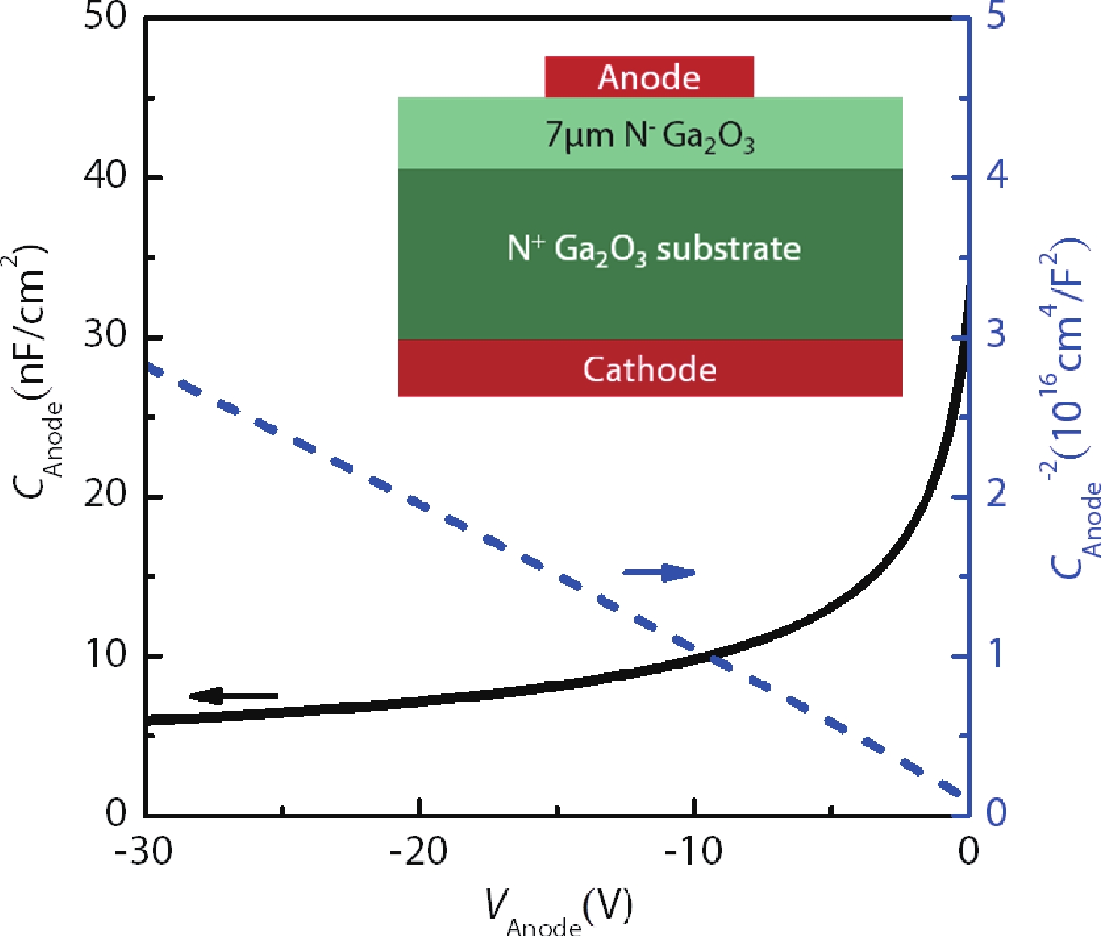
Fig. 1.
(Color online) Cross-sectional schematic of the devices with DL-JTE/ JTE.
ARTICLES
Tingting Han§, Yuangang Wang§, Yuanjie Lv, Shaobo Dun, Hongyu Liu, Aimin Bu and Zhihong Feng
Corresponding author: Yuanjie Lv, yuanjielv@163.com; Zhihong Feng, ga917vv@163.com
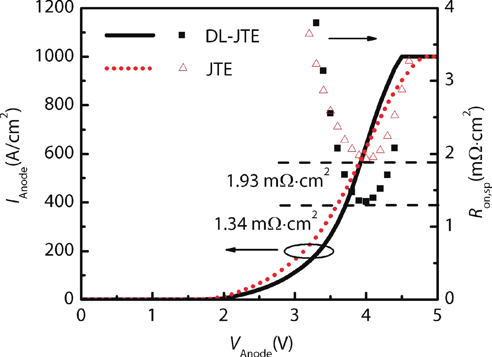
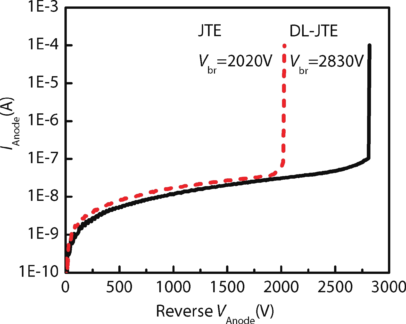
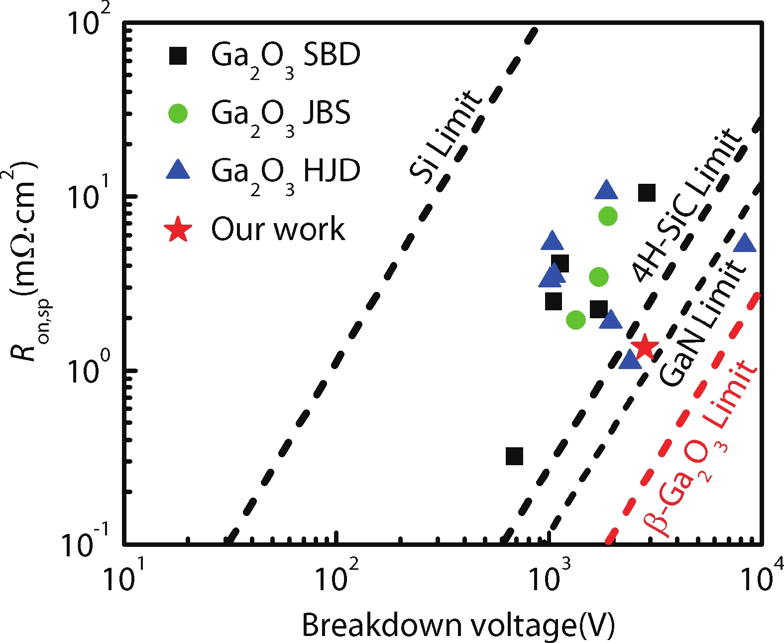
Abstract: This work demonstrates high-performance NiO/β-Ga2O3 vertical heterojunction diodes (HJDs) with double-layer junction termination extension (DL-JTE) consisting of two p-typed NiO layers with varied lengths. The bottom 60-nm p-NiO layer fully covers the β-Ga2O3 wafer, while the geometry of the upper 60-nm p-NiO layer is 10 μm larger than the square anode electrode. Compared with a single-layer JTE, the electric field concentration is inhibited by double-layer JTE structure effectively, resulting in the breakdown voltage being improved from 2020 to 2830 V. Moreover, double p-typed NiO layers allow more holes into the Ga2O3 drift layer to reduce drift resistance. The specific on-resistance is reduced from 1.93 to 1.34 mΩ·cm2. The device with DL-JTE shows a power figure-of-merit (PFOM) of 5.98 GW/cm2, which is 2.8 times larger than that of the conventional single-layer JTE structure. These results indicate that the double-layer JTE structure provides a viable way of fabricating high-performance Ga2O3 HJDs.
Key words: β-Ga2O3, breakdown voltage, heterojunction diode (HJD), junction termination extension (JTE), power figure-of-merit (PFOM)
| [1] |
Zhang H Z, Wang L J, Xia C T, et al. Research progress of wide-gap semiconductor β-Ga2O3 single crystal. J Synth Cryst, 2015, 44, 2943 doi: 10.1109/TPEL.2019.2946367
|
| [2] |
Hu Z Z, Lv Y J, Zhao C Y, et al. Beveled fluoride plasma treatment for vertica β-Ga2O3 Schottky barrier diode with high reverse blocking voltage and low turn-on voltage. IEEE Electron Device Lett, 2020, 41(3), 441 doi: 10.1109/LED.2020.2968587
|
| [3] |
Xiong W H, Zhou X Z, Xu G W, et al. Double-barrier β-Ga2O3 Schottky barrier diode with low turn-on voltage and leakage current. IEEE Electron Device Lett, 2021, 42(3), 430 doi: 10.1109/LED.2021.3055349
|
| [4] |
Saurav R, Arkka B, Praneeth R, et al. High-k oxide field-plated vertical (001) β-Ga2O3 Schottky barrier diode with Baliga’s figure of merit over 1 GW/cm2. IEEE Electron Device Lett, 2021, 42(8), 1140 doi: 10.1109/LED.2021.3089945
|
| [5] |
He Q M, Hao W B, Zhou X Z, et al. Over 1 GW/cm2 vertical Ga2O3 Schottky barrier diodes without edge termination. IEEE Electron Device Lett, 2022, 43(2), 264 doi: 10.1109/LED.2021.3133866
|
| [6] |
Li W S, Kazuki N, Hu Z Y, et al. Field-plated Ga2O3 trench Schottky barrier diodes with a BV2/Ron, sp of up to 0.95 GW/cm2. IEEE Electron Device Lett, 2020, 41(1), 107 doi: 10.1109/LED.2019.2953559
|
| [7] |
Tetzner K, Treidel E B, Hilt O, et al. Lateral 1.8 KV β-Ga2O3 MOSFET with 155 MW/cm2 power figure of merit. IEEE Electron Device Lett, 2019, 40(9), 1503 doi: 10.1109/LED.2019.2930189
|
| [8] |
Lv Y J, Liu H Y, Zhou X Y, et al. Lateral β-Ga2O3 MOSFETs with high power figure of merit of 277 MW/cm2. IEEE Electron Device Lett, 2020, 41(4), 537 doi: 10.1109/LED.2020.2974515
|
| [9] |
Hu Z Y, Nomoto K, Li W S, et al. Enhancement-mode Ga2O3 vertical transistors with breakdown voltage >1 kV. IEEE Electron Device Lett, 2018, 39(6), 869 doi: 10.1109/LED.2018.2830184
|
| [10] |
Sharma S, Zeng K, Saha S, et al. Field-plated lateral Ga2O3 MOSFETs with polymer passivation and 8.03 kV breakdown voltage. IEEE Electron Device Lett, 2020, 41(6), 836 doi: 10.1109/LED.2020.2991146
|
| [11] |
Zheng Z Y, Qiao B S, Zhang Z Z, et al. High detectivity of metal–semiconductor–metal Ga2O3 solar-blind photodetector through thickness-regulated gain. IEEE Trans Electron Devices, 2022, 69(8), 4362 doi: 10.1109/TED.2022.3184277
|
| [12] |
Qiao B S, Zhang Z Z, Xie X H, et al. Quenching of persistent photocurrent in an oxide UV photodetector. J Mater Chem C, 2021, 9, 4039 doi: 10.1039/D0TC05997H
|
| [13] |
Yoshihiro K, Shohei K, Shinji N. All-oxide p–n heterojunction diodes comprising p-type NiO and n-type β-Ga2O3. Appl Phys Express, 2016, 9(9), 091101 doi: 10.7567/APEX.9.091101
|
| [14] |
Gong H H, Chen X H, Xu Y, et al. A 1.86-kV double-layered NiO/β-Ga2O3 vertical p–n heterojunction diode. Appl Phys Lett, 2020, 117, 022104 doi: 10.1063/5.0010052
|
| [15] |
Lu X, Zhou X D, Jiang H X, et al. 1-kV sputtered p-NiO/n-Ga2O3 heterojunction diodes with an ultra-low leakage current below 1 μA/cm2. IEEE Electron Device Lett, 2020, 41(3), 449 doi: 10.1109/LED.2020.2967418
|
| [16] |
Gong H H, Zhou F, Xu W Z, et al. 1.37 kV/12 A NiO/β-Ga2O3 heterojunction diode with nanosecond reverse recovery and rugged surge-current capability. IEEE Trans Power Eletron, 2021, 36(11), 12213 doi: 10.1109/TPEL.2021.3082640
|
| [17] |
Gong H H, Wang Z P, Yu X X, et al. Field-plated NiO/Ga2O3 p-n heterojunction power diodes with high-temperature thermal stability and near unity ideality factors. Electron Device Soc, 2021, 9, 1166 doi: 10.1109/JEDS.2021.3130305
|
| [18] |
Zhou F, Gong H H, Xu W Z, et al. 1.95-kV Beveled-mesa NiO/β-Ga2O3 heterojunction diode with 98.5% conversion efficiency and over million-times overvoltage ruggedness. IEEE Trans Power Eletronics, 2022, 37(2), 1223 doi: 10.1109/TPEL.2021.3108780
|
| [19] |
Hu Z Z, Li J G, Zhao C Y, et al. Design and fabrication of vertical metal/TiO2/β-Ga2O3 dielectric heterojunction diode with reverse blocking voltage of 1010 V. IEEE Trans Electron Devices, 2020, 67(12), 5628 doi: 10.1109/TED.2020.3033787
|
| [20] |
Wang Y G, Gong H H, Lv Y J, et al. 2.41 kV vertical p-NiO/n-Ga2O3 heterojunction diodes with a record Baliga’s figure-of-merit of 5.18 GW/cm2. IEEE Trans Power Eletronics, 2022, 37(4), 3743 doi: 10.1109/TPEL.2021.3123940
|
| [21] |
Zhang J C, Dong P F, Dang K, et al. Ultra-wide bandgap semiconductor Ga2O3 power diodes. Nat Commun, 2022, 13, 3900 doi: 10.1038/s41467-022-31664-y
|
| [22] |
Yan Q L, Gong H H, Zhang J C, et al. β-Ga2O3 hetero-junction barrier Schottky diode with reverse leakage current modulation and BV2/Ron,sp value of 0.93 GW/cm2. Appl Phys Lett, 2021, 118, 122102 doi: 10.1063/5.0044130
|
| [23] |
Gong H H, Yu X X, Xu Y, et al. β-Ga2O3 vertical heterojunction barrier Schottky diodes terminated with p-NiO field limiting rings. Appl Phys Lett, 2021, 118, 202102 doi: 10.1063/5.0050919
|
| [24] |
Lv Y J, Wang Y G, Fu X C, et al. Demonstration of β-Ga2O3 junction barrier Schottky diodes with a Baliga’s figure of merit of 0.85 GW/cm2 or a 5A/700 V handling capabilities. IEEE Trans Power Eletronics, 2021, 36(6), 6179 doi: 10.1109/TPEL.2020.3036442
|


Article views: 1337 Times PDF downloads: 178 Times Cited by: 0 Times
Received: 08 December 2022 Revised: 18 January 2023 Online: Accepted Manuscript: 18 February 2023Uncorrected proof: 20 February 2023Corrected proof: 12 June 2023Published: 10 July 2023
| Citation: |
Tingting Han, Yuangang Wang, Yuanjie Lv, Shaobo Dun, Hongyu Liu, Aimin Bu, Zhihong Feng. 2.83-kV double-layered NiO/β-Ga2O3 vertical p-n heterojunction diode with a power figure-of-merit of 5.98 GW/cm2[J]. Journal of Semiconductors, 2023, 44(7): 072802. doi: 10.1088/1674-4926/44/7/072802
****
T T Han, Y G Wang, Y J Lv, S B Dun, H Y Liu, A M Bu, Z H Feng. 2.83-kV double-layered NiO/β-Ga2O3 vertical p-n heterojunction diode with a power figure-of-merit of 5.98 GW/cm2[J]. J. Semicond, 2023, 44(7): 072802. doi: 10.1088/1674-4926/44/7/072802

|
 Tingting Han:was born in Hengshui, Hebei Province in 1986, senior engineer with a master's degree in microelectronics and solid state electronics. She graduated from Shandong University in 2011, mainly works in the research of gallium oxide devices
 Yuanjie Lv:was born in Tai'an City, Shandong Province in 1985, professor. He got doctor’s degree in microelectronics and solid-state electronics from Shandong University in 2012. He mainly works in the research of wide-gap semiconductor electronic devices
| [1] |
Zhang H Z, Wang L J, Xia C T, et al. Research progress of wide-gap semiconductor β-Ga2O3 single crystal. J Synth Cryst, 2015, 44, 2943 doi: 10.1109/TPEL.2019.2946367
|
| [2] |
Hu Z Z, Lv Y J, Zhao C Y, et al. Beveled fluoride plasma treatment for vertica β-Ga2O3 Schottky barrier diode with high reverse blocking voltage and low turn-on voltage. IEEE Electron Device Lett, 2020, 41(3), 441 doi: 10.1109/LED.2020.2968587
|
| [3] |
Xiong W H, Zhou X Z, Xu G W, et al. Double-barrier β-Ga2O3 Schottky barrier diode with low turn-on voltage and leakage current. IEEE Electron Device Lett, 2021, 42(3), 430 doi: 10.1109/LED.2021.3055349
|
| [4] |
Saurav R, Arkka B, Praneeth R, et al. High-k oxide field-plated vertical (001) β-Ga2O3 Schottky barrier diode with Baliga’s figure of merit over 1 GW/cm2. IEEE Electron Device Lett, 2021, 42(8), 1140 doi: 10.1109/LED.2021.3089945
|
| [5] |
He Q M, Hao W B, Zhou X Z, et al. Over 1 GW/cm2 vertical Ga2O3 Schottky barrier diodes without edge termination. IEEE Electron Device Lett, 2022, 43(2), 264 doi: 10.1109/LED.2021.3133866
|
| [6] |
Li W S, Kazuki N, Hu Z Y, et al. Field-plated Ga2O3 trench Schottky barrier diodes with a BV2/Ron, sp of up to 0.95 GW/cm2. IEEE Electron Device Lett, 2020, 41(1), 107 doi: 10.1109/LED.2019.2953559
|
| [7] |
Tetzner K, Treidel E B, Hilt O, et al. Lateral 1.8 KV β-Ga2O3 MOSFET with 155 MW/cm2 power figure of merit. IEEE Electron Device Lett, 2019, 40(9), 1503 doi: 10.1109/LED.2019.2930189
|
| [8] |
Lv Y J, Liu H Y, Zhou X Y, et al. Lateral β-Ga2O3 MOSFETs with high power figure of merit of 277 MW/cm2. IEEE Electron Device Lett, 2020, 41(4), 537 doi: 10.1109/LED.2020.2974515
|
| [9] |
Hu Z Y, Nomoto K, Li W S, et al. Enhancement-mode Ga2O3 vertical transistors with breakdown voltage >1 kV. IEEE Electron Device Lett, 2018, 39(6), 869 doi: 10.1109/LED.2018.2830184
|
| [10] |
Sharma S, Zeng K, Saha S, et al. Field-plated lateral Ga2O3 MOSFETs with polymer passivation and 8.03 kV breakdown voltage. IEEE Electron Device Lett, 2020, 41(6), 836 doi: 10.1109/LED.2020.2991146
|
| [11] |
Zheng Z Y, Qiao B S, Zhang Z Z, et al. High detectivity of metal–semiconductor–metal Ga2O3 solar-blind photodetector through thickness-regulated gain. IEEE Trans Electron Devices, 2022, 69(8), 4362 doi: 10.1109/TED.2022.3184277
|
| [12] |
Qiao B S, Zhang Z Z, Xie X H, et al. Quenching of persistent photocurrent in an oxide UV photodetector. J Mater Chem C, 2021, 9, 4039 doi: 10.1039/D0TC05997H
|
| [13] |
Yoshihiro K, Shohei K, Shinji N. All-oxide p–n heterojunction diodes comprising p-type NiO and n-type β-Ga2O3. Appl Phys Express, 2016, 9(9), 091101 doi: 10.7567/APEX.9.091101
|
| [14] |
Gong H H, Chen X H, Xu Y, et al. A 1.86-kV double-layered NiO/β-Ga2O3 vertical p–n heterojunction diode. Appl Phys Lett, 2020, 117, 022104 doi: 10.1063/5.0010052
|
| [15] |
Lu X, Zhou X D, Jiang H X, et al. 1-kV sputtered p-NiO/n-Ga2O3 heterojunction diodes with an ultra-low leakage current below 1 μA/cm2. IEEE Electron Device Lett, 2020, 41(3), 449 doi: 10.1109/LED.2020.2967418
|
| [16] |
Gong H H, Zhou F, Xu W Z, et al. 1.37 kV/12 A NiO/β-Ga2O3 heterojunction diode with nanosecond reverse recovery and rugged surge-current capability. IEEE Trans Power Eletron, 2021, 36(11), 12213 doi: 10.1109/TPEL.2021.3082640
|
| [17] |
Gong H H, Wang Z P, Yu X X, et al. Field-plated NiO/Ga2O3 p-n heterojunction power diodes with high-temperature thermal stability and near unity ideality factors. Electron Device Soc, 2021, 9, 1166 doi: 10.1109/JEDS.2021.3130305
|
| [18] |
Zhou F, Gong H H, Xu W Z, et al. 1.95-kV Beveled-mesa NiO/β-Ga2O3 heterojunction diode with 98.5% conversion efficiency and over million-times overvoltage ruggedness. IEEE Trans Power Eletronics, 2022, 37(2), 1223 doi: 10.1109/TPEL.2021.3108780
|
| [19] |
Hu Z Z, Li J G, Zhao C Y, et al. Design and fabrication of vertical metal/TiO2/β-Ga2O3 dielectric heterojunction diode with reverse blocking voltage of 1010 V. IEEE Trans Electron Devices, 2020, 67(12), 5628 doi: 10.1109/TED.2020.3033787
|
| [20] |
Wang Y G, Gong H H, Lv Y J, et al. 2.41 kV vertical p-NiO/n-Ga2O3 heterojunction diodes with a record Baliga’s figure-of-merit of 5.18 GW/cm2. IEEE Trans Power Eletronics, 2022, 37(4), 3743 doi: 10.1109/TPEL.2021.3123940
|
| [21] |
Zhang J C, Dong P F, Dang K, et al. Ultra-wide bandgap semiconductor Ga2O3 power diodes. Nat Commun, 2022, 13, 3900 doi: 10.1038/s41467-022-31664-y
|
| [22] |
Yan Q L, Gong H H, Zhang J C, et al. β-Ga2O3 hetero-junction barrier Schottky diode with reverse leakage current modulation and BV2/Ron,sp value of 0.93 GW/cm2. Appl Phys Lett, 2021, 118, 122102 doi: 10.1063/5.0044130
|
| [23] |
Gong H H, Yu X X, Xu Y, et al. β-Ga2O3 vertical heterojunction barrier Schottky diodes terminated with p-NiO field limiting rings. Appl Phys Lett, 2021, 118, 202102 doi: 10.1063/5.0050919
|
| [24] |
Lv Y J, Wang Y G, Fu X C, et al. Demonstration of β-Ga2O3 junction barrier Schottky diodes with a Baliga’s figure of merit of 0.85 GW/cm2 or a 5A/700 V handling capabilities. IEEE Trans Power Eletronics, 2021, 36(6), 6179 doi: 10.1109/TPEL.2020.3036442
|

 WeChat ID
Journal of Semiconductors © 2017 All Rights Reserved 京ICP备05085259号-2

 DownLoad:

