


Although perovskite solar cells (PSCs) demonstrate outstanding power conversion efficiency (PCE), their practical applications are still limited by stability issues caused by various problems such as poor crystal quality triggered structural instability. Herein, to address the structural instability of perovskites, we introduced a polymer additive, poly-L-lysine hydrobromide (PLL), into the perovskite precursor to promote perovskite crystal growth, thereby constructing a stable crystal structure. The results show that the introduction of PLL modulates the colloidal aggregation state in the precursor solution, provides longer time for growth of perovskite and successfully realizes the formation of large-sized perovskite films with high crystallinity. More importantly, owing to its hydrophobic long-chain structure and the widespread distribution of C=O and NH on the chain, PLL firmly locks the perovskite crystals, enhancing their structural stability while blocking the intrusion of external factors such as water molecules, significantly enhances the overall stability of the device. The results show that the PLL-based PSC has negligible hysteresis and its PCE is improved from 22.20% to 23.66%. while the PLL-modified perovskite films and devices demonstrate excellent thermal and environmental stability. These findings highlight PLL as a promising additive for optimizing perovskite crystallization, offering guidance for fabricating efficient and stable photovoltaic devices.
- • Uncorrected proofs: articles that have been copy edited and formatted, but have not been finalized yet. They still need to be proof-read and corrected by the author(s) and the text could still change before final publication.
- • Corrected proofs: articles that contain the authors' corrections. Final citation details, e.g. volume and/or issue number, publication year and page numbers, still need to be added and the text might change before final publication.
There are two types in Press articles:


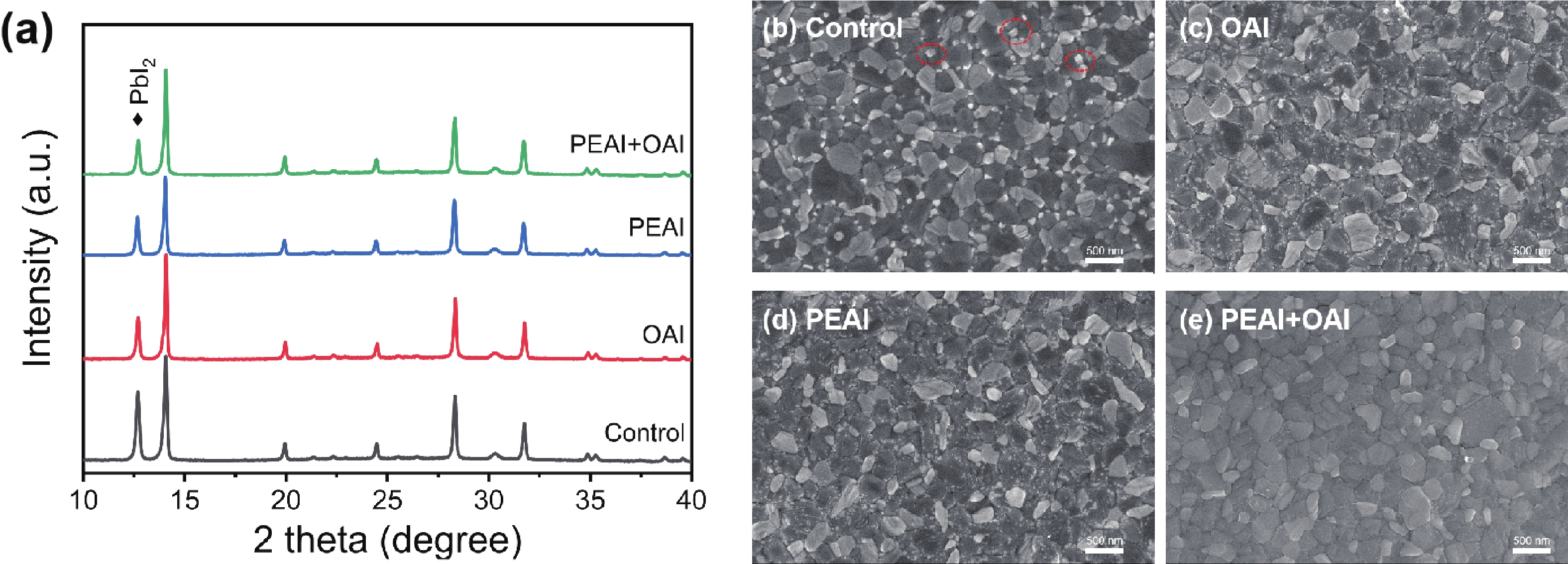
Interfacial defects and environmental instability at perovskite surfaces pose significant challenges for inverted perovskite solar cells (PSCs). Surface post-treatment strategies have emerged as a viable approach to improve film quality and passivate defects. Although organic molecules can passivate both surfaces and grain boundaries via hydrogen or covalent bonding, their limited adsorption specificity often results in incomplete defect neutralization. In this work, we introduce a bilayer passivation approach employing phenethylammonium iodide (PEAI) and n-octylammonium iodide (OAI) to concurrently mitigate non-radiative recombination and improve stability. PEAI passivates undercoordinated Pb2+ at grain boundaries and surfaces, effectively eliminating deep-level traps and suppressing non-radiative losses. Meanwhile, OAI forms a hydrophobic barrier on the perovskite surface through its long alkyl chains, inhibiting moisture penetration without compromising interfacial charge transport. As a result, the perovskite film exhibits significantly enhanced optoelectronic performance and environmental stability, achieving a champion power conversion efficiency (PCE) of 24.48%.


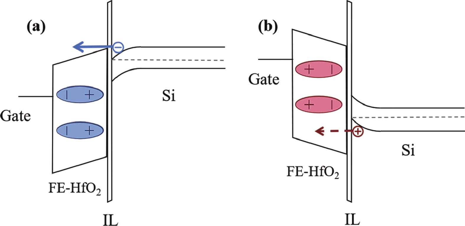
The novel HfO2-based ferroelectric field effect transistor (FeFET) is considered a promising candidate for next-generation nonvolatile memory (NVM). However, a series of reliability issues caused by the fatigue effect hinder its further development. Therefore, a comprehensive understanding of the fatigue mechanisms of the device and optimization strategies is essential for its application. The fundamental mechanism of the fatigue effect is attributed to charge trapping and trap generation based on the current studies, and the underlying causes, occurrence locations and specific impacts are analyzed in this review. In particular, the asymmetric trapping/detrapping of electrons and holes, as well as the relationship between the ferroelectric (FE) polarization and charge trapping, are given particular attention. After categorizing and summarizing the current progress, we propose a series of optimization strategies derived based on the fatigue mechanisms.


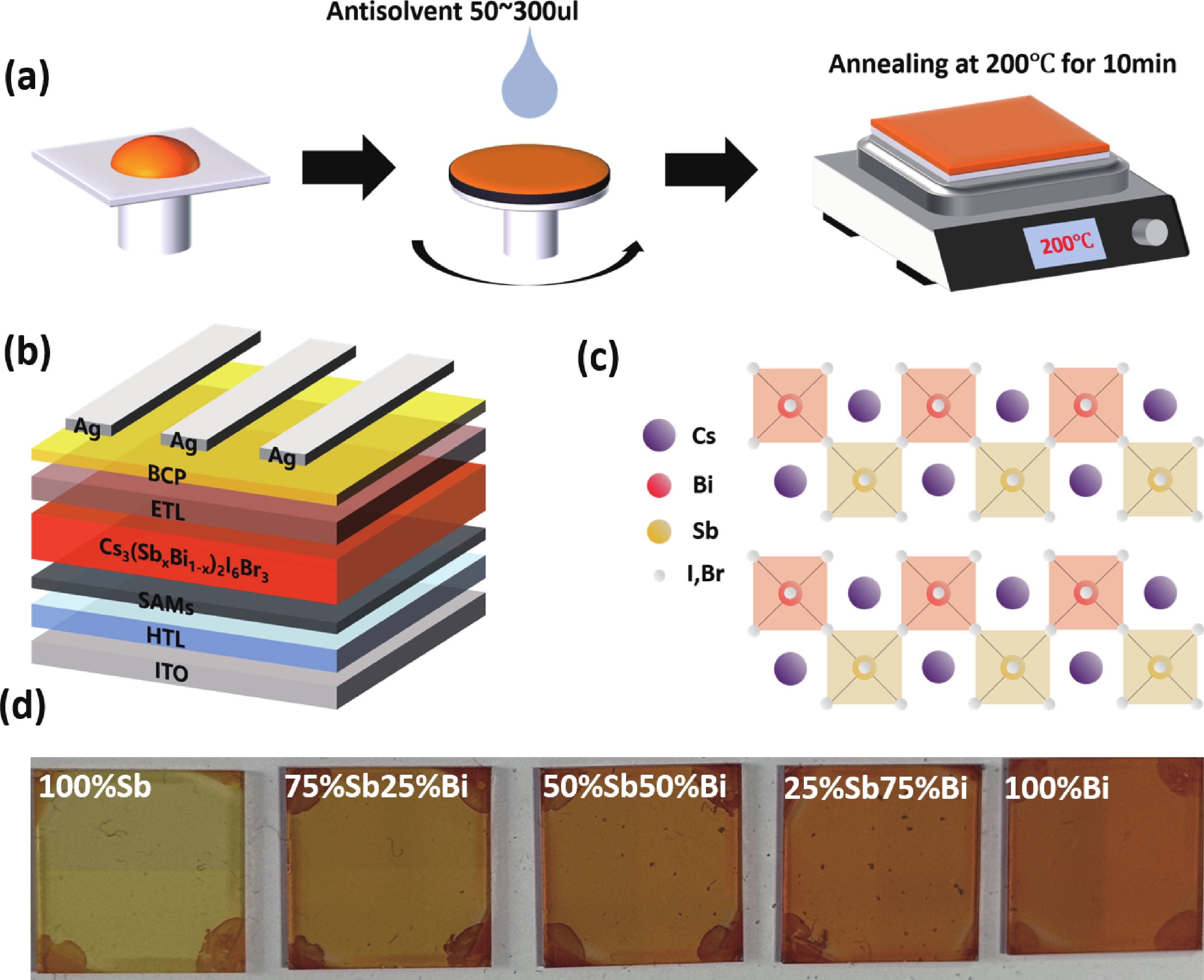
Owing to their low toxicity and remarkable stability, perovskites based on antimony and bismuth have garnered significant interest in recent years. However, A3B2X9 perovskite materials derived from antimony and bismuth face several challenges, including excessively wide band gaps, elevated defect densities, and suboptimal film quality, all of which hinder advancements in device efficiency. While extensive studies have been undertaken to investigate the effects of modulating the A-site and X-site elements in lead-free A3B2X9 perovskites, there remains a notable scarcity of reports addressing the impact of modifications to the B-site element. In this study, we investigated the alloying of antimony and bismuth within the 2D Cs3B2I6Br3 perovskite. By systematically varying the ratios of two elements, we found that the incorporation of both antimony and bismuth at the B-site significantly enhances the quality of the perovskite films. Our findings indicate that a 1 : 1 ratio of antimony to bismuth produces the densest films, the highest photoluminescence intensity, and superior photovoltaic performance. Ultimately, the devices fabricated using this optimal ratio achieved an open-circuit voltage (VOC) of 1.01 V and a power conversion efficiency (PCE) of 0.645%.


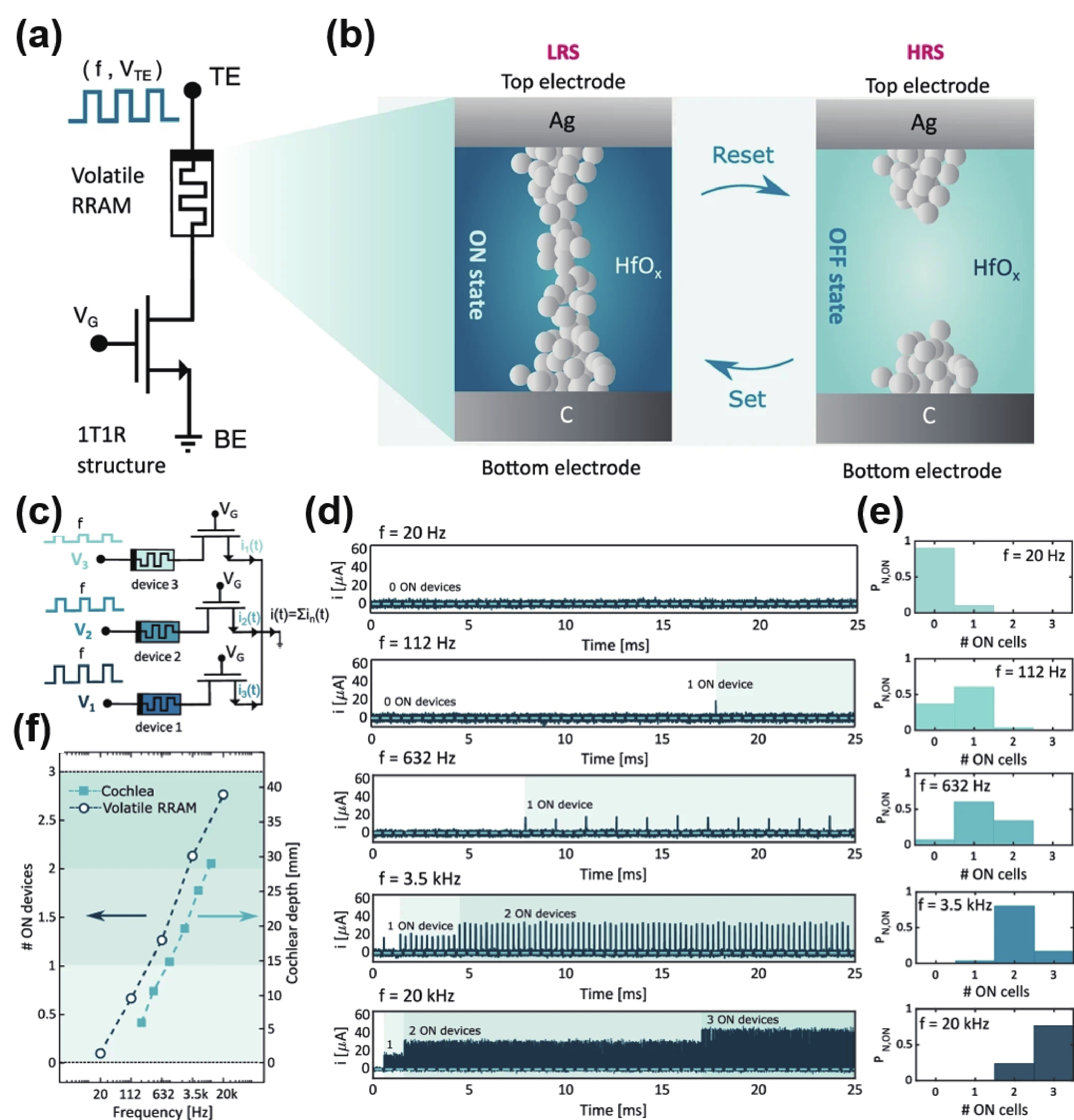
As traditional von Neumann architectures face limitations in handling the demands of big data and complex computational tasks, neuromorphic computing has emerged as a promising alternative, inspired by the human brain's neural networks. Volatile memristors, particularly Mott and diffusive memristors, have garnered significant attention for their ability to emulate neuronal dynamics, such as spiking and firing patterns, enabling the development of reconfigurable and adaptive computing systems. Recent advancements include the implementation of leaky integrate-and-fire neurons, Hodgkin−Huxley neurons, optoelectronic neurons, and time-surface neurons, all utilizing volatile memristors to achieve efficient, low-power, and highly integrated neuromorphic systems. This paper reviews the latest progress in volatile memristor-based artificial neurons, highlighting their potential for energy-efficient computing and integration with artificial synapses. We conclude by addressing challenges such as improving memristor reliability and exploring new architectures to advance memristor-based neuromorphic computing.


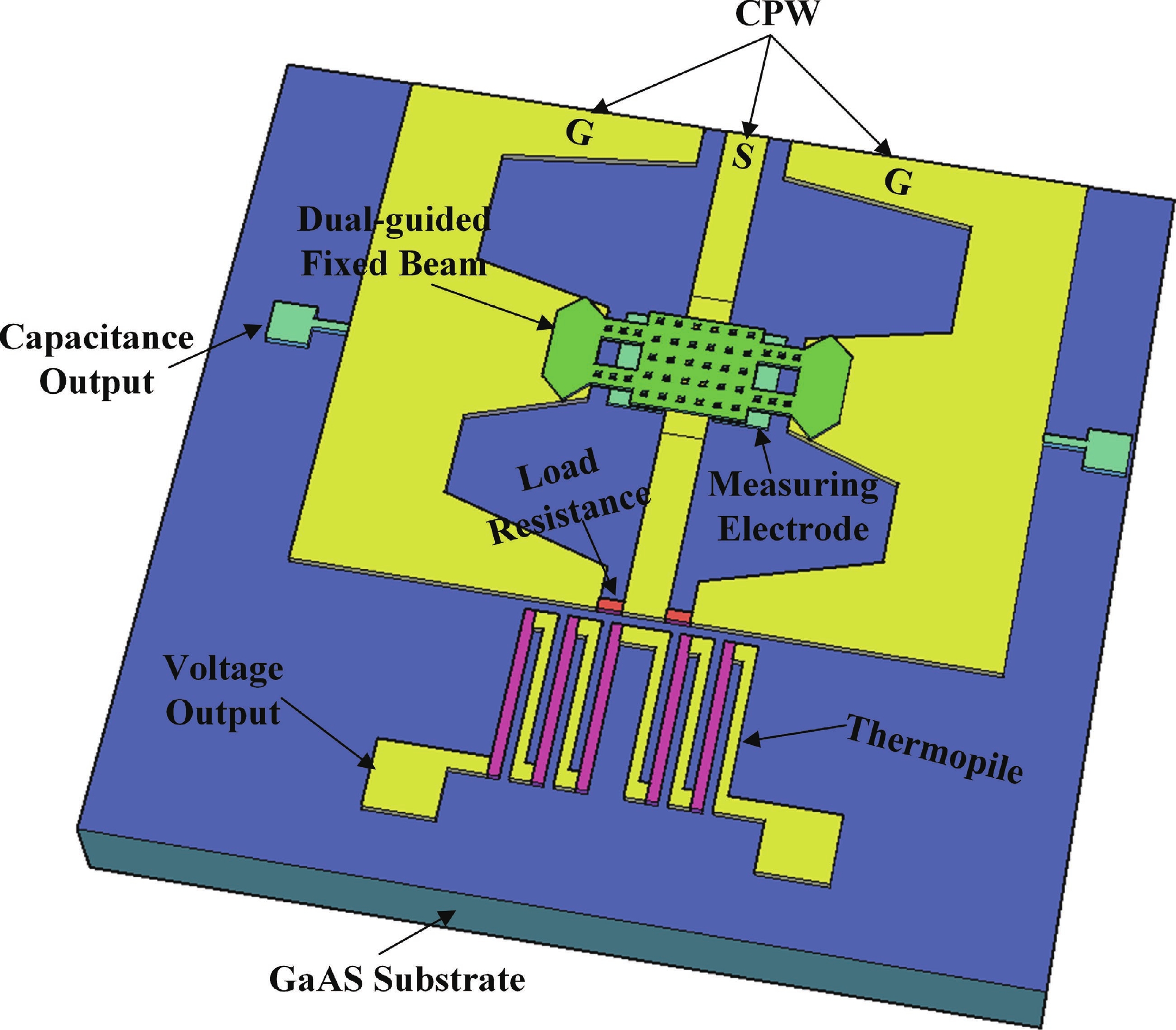
In order to solve the problems of low overload power in MEMS cantilever beams and low sensitivity in traditional MEMS fixed beams, a novel MEMS microwave power detection chip based on the dual-guided fixed beam is designed. A gap between guiding beams and measuring electrodes is designed to accelerate the release of the sacrificial layer, effectively enhancing chip performance. A load sensing model for the MEMS fixed beam microwave power detection chip is proposed, and the mechanical characteristics are analyzed based on the uniform load applied. The overload power and sensitivity are investigated using the load sensing model, and experimental results are compared with theoretical results. The detection chip exhibits excellent microwave characteristic in the 9−11 GHz frequency band, with a return loss less than −10 dB. At a signal frequency of 10 GHz, the theoretical sensitivity is 13.8 fF/W, closely matching the measured value of 14.3 fF/W, with a relative error of only 3.5%. These results demonstrate that the proposed load sensing model provides significant theoretical support for the design and performance optimization of MEMS microwave power detection chips.


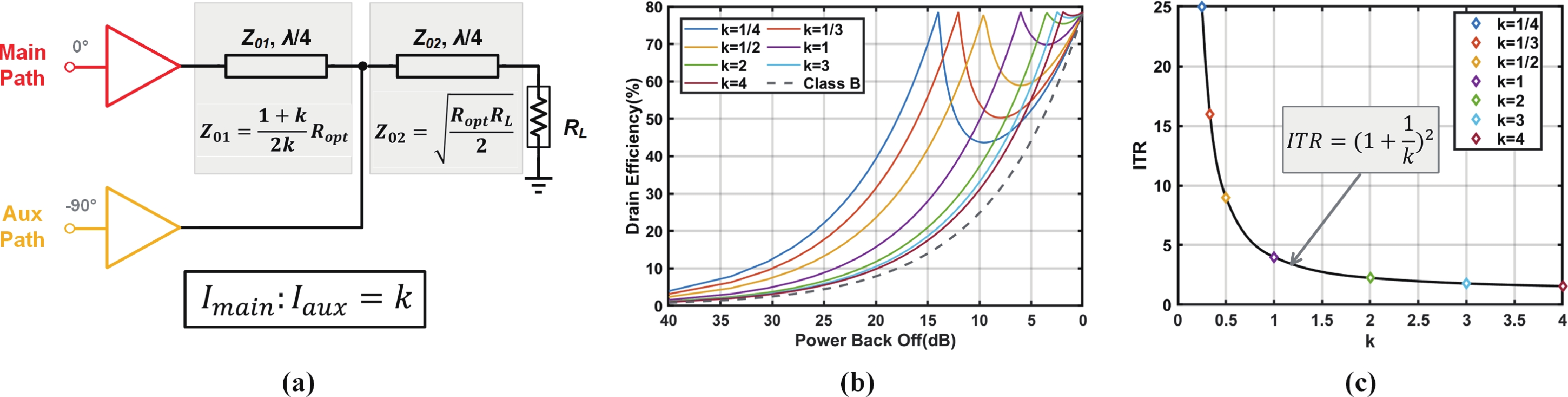
A two-way K/Ka-band series-Doherty PA (SDPA) with a distributed impedance inverting network (IIN) for millimeter wave applications is presented in this article. The proposed distributed IIN contributes to achieve wideband linear and power back-off (PBO) efficiency enhancement. Implemented in 65 nm bulk CMOS technology, this work realizes a measured 3 dB bandwidth of 15.5 GHz with 21.2 dB peak small-signal gain at 34.2 GHz. Under 1-V power supply, it achieves OP1dB over 13.4 dBm and Psat over 16 dBm between 21 to 30 GHz. The measured maximum Psat, OP1dB, peak/OP1dB/6dBPBO PAE results are 17.5, 14.7 dBm, and 28.2%/23.2%/13.2%. Without digital pre-distortion (DPD) and equalization, EVMs are lower than −25.2 dB for 200 MHz 64-QAM signals. Besides, this work achieves −33.35, −23.52, and −20 dB EVMs for 100 MHz 256-QAM, 600 MHz 64-QAM and 2 GHz 16-QAM signals at 27 GHz without DPD and equalization.


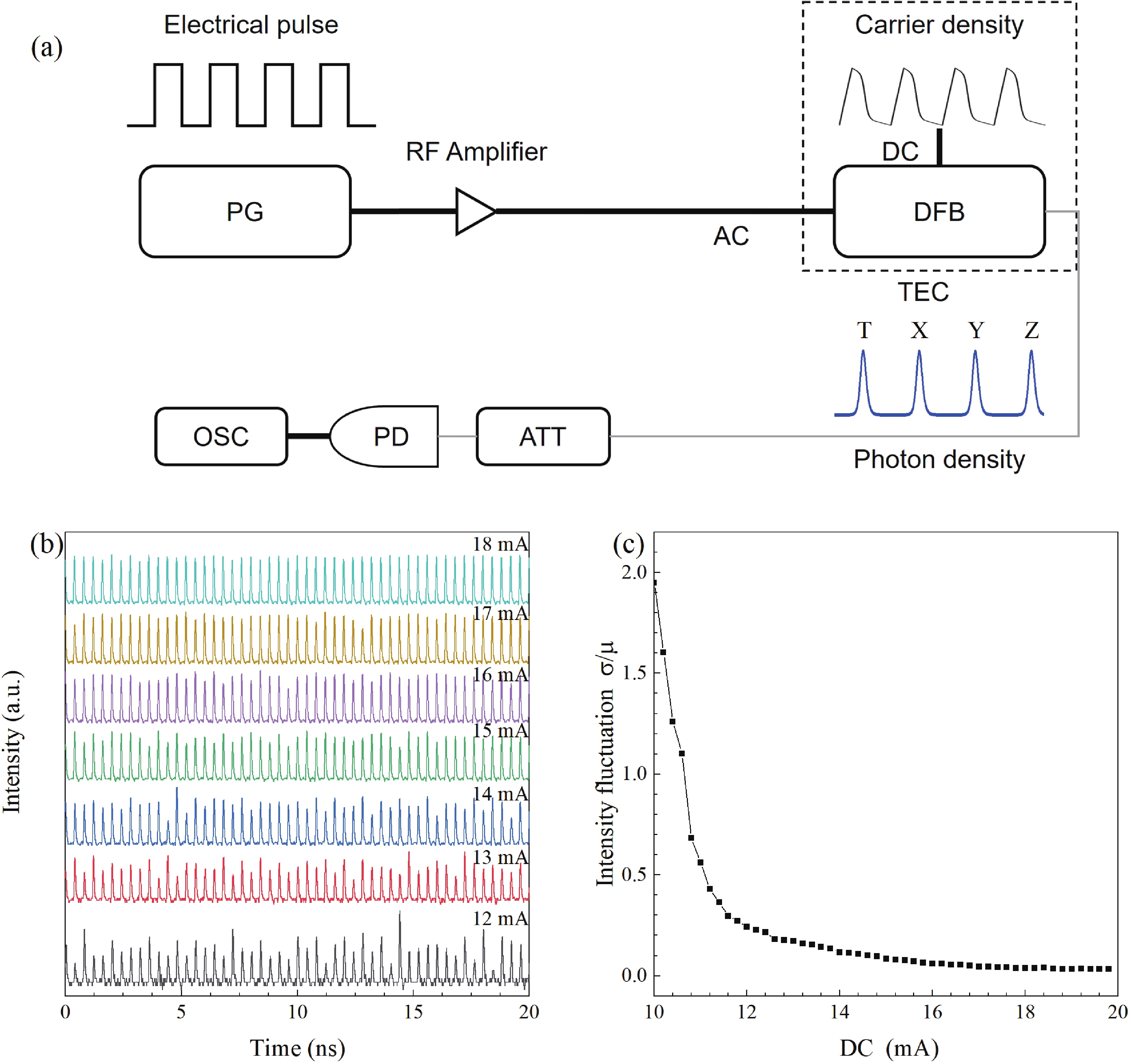
In the implementation of quantum key distribution, Security certification is a prerequisite for social deployment. Transmitters in decoy-BB84 systems typically employ gain-switched semiconductor lasers (GSSLs) to generate optical pulses for encoding quantum information. However, the working state of the laser may violate the assumption of pulse independence. Here, we explored the dependence of intensity fluctuation and high-order correlation distribution of optical pulses on driving currents at 2.5 GHz. We found the intensity correlation distribution had a significant dependence on the driving currents, which would affect the final key rate. By utilizing rate equations in our simulation, we confirmed the fluctuation and correlation originated from the instability of gain-switched laser driven at a GHz-repetitive frequency. Finally, we evaluated the impact of intensity fluctuation on the secure key rate. This work will provide valuable insights for assessing whether the transmitter is operating at optimal state in practice.


In this paper, a high-gain inductorless LNA (low-noise amplifier) compatible with multiple communication protocols from 0.1 to 5.1 GHz is proposed. A composite resistor−capacitor feedback structure is employed to achieve a wide bandwidth matching range and good gain flatness. A second stage with a Darlington pair is used to increase the overall gain of the amplifier, while the gain of the first stage is reduced to reduce the overall noise. The amplifier is based on a 0.25 μm SiGe BiCMOS process, and thanks to the inductorless circuit structure, the core circuit area is only 0.03 mm2. Test results show that the lowest noise figure (NF) in the operating band is 1.99 dB, the power gain reaches 29.7 dB, the S11 and S22 are less than −10 dB, the S12 is less than −30 dB, the IIP3 is 0.81dBm, and the OP1dB is 10.27 dBm. The operating current is 31.18 mA at 3.8 V supply.


Infrared and terahertz waves constitute pivotal bands within the electromagnetic spectrum, distinguished by their robust penetration capabilities and non-ionizing nature. These wavebands offer the potential for achieving high-resolution and non-destructive detection methodologies, thereby possessing considerable research significance across diverse domains including communication technologies, biomedical applications, and security screening systems. Two-dimensional materials, owing to their distinctive optoelectronic attributes, have found widespread application in photodetection endeavors. Nonetheless, their efficacy diminishes when tasked with detecting lower photon energies. Furthermore, as the landscape of device integration evolves, two-dimensional materials struggle to align with the stringent demands for device superior performance. Topological materials, with their topologically protected electronic states and non-trivial topological invariants, exhibit quantum anomalous Hall effects and ultra-high carrier mobility, providing a new approach for seeking photosensitive materials for infrared and terahertz photodetectors. This article introduces various types of topological materials and their properties, followed by an explanation of the detection mechanism and performance parameters of photodetectors. Finally, it summarizes the current research status of near-infrared to far-infrared photodetectors and terahertz photodetectors based on topological materials, discussing the challenges faced and future prospects in their development.


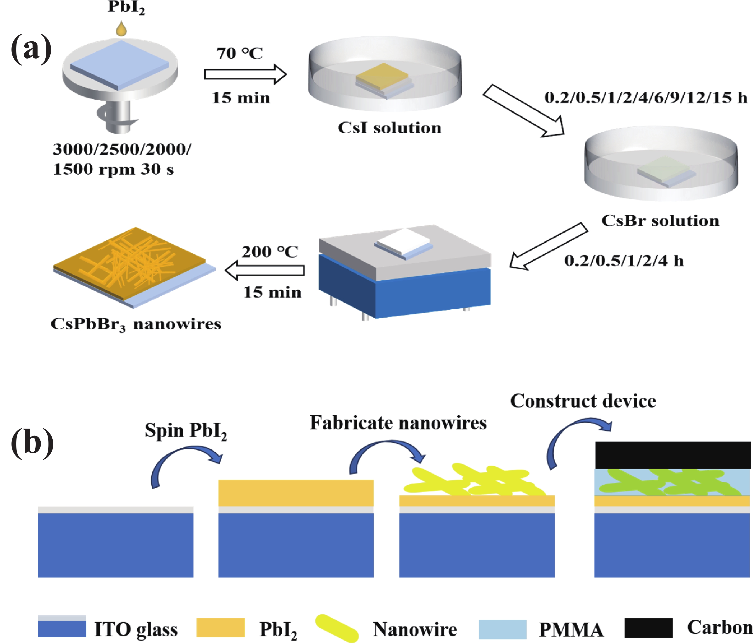
High-performance perovskite photodetectors with self-driven characteristic usually need electron/hole transport layers to extract carriers. However, these devices with transport layer structure are prone to result in a poor perovskite/transport layer interface, which restricts the performance and stability of the device. To solve this problem, this work reports a novel device structure in which perovskite nanowires are in-situ prepared on PbI2, which serves as both a reaction raw material and efficient carrier extraction layer. By optimizing the thickness of PbI2, nanowire growth time, and ion exchange time, a self-driven photodetector with an ITO/PbI2/CsPbBr3/carbon structure is constructed. The optimized device achieves excellent performance with the responsivity of 0.33 A/W, the detectivity of as high as 3.52 × 10¹³ Jones. Furthermore, the device can detect the light with its optical power lowered to 0.1 nW/cm2. This research provides a new method for preparing perovskite nano/micro devices with simple structure but excellent performance.


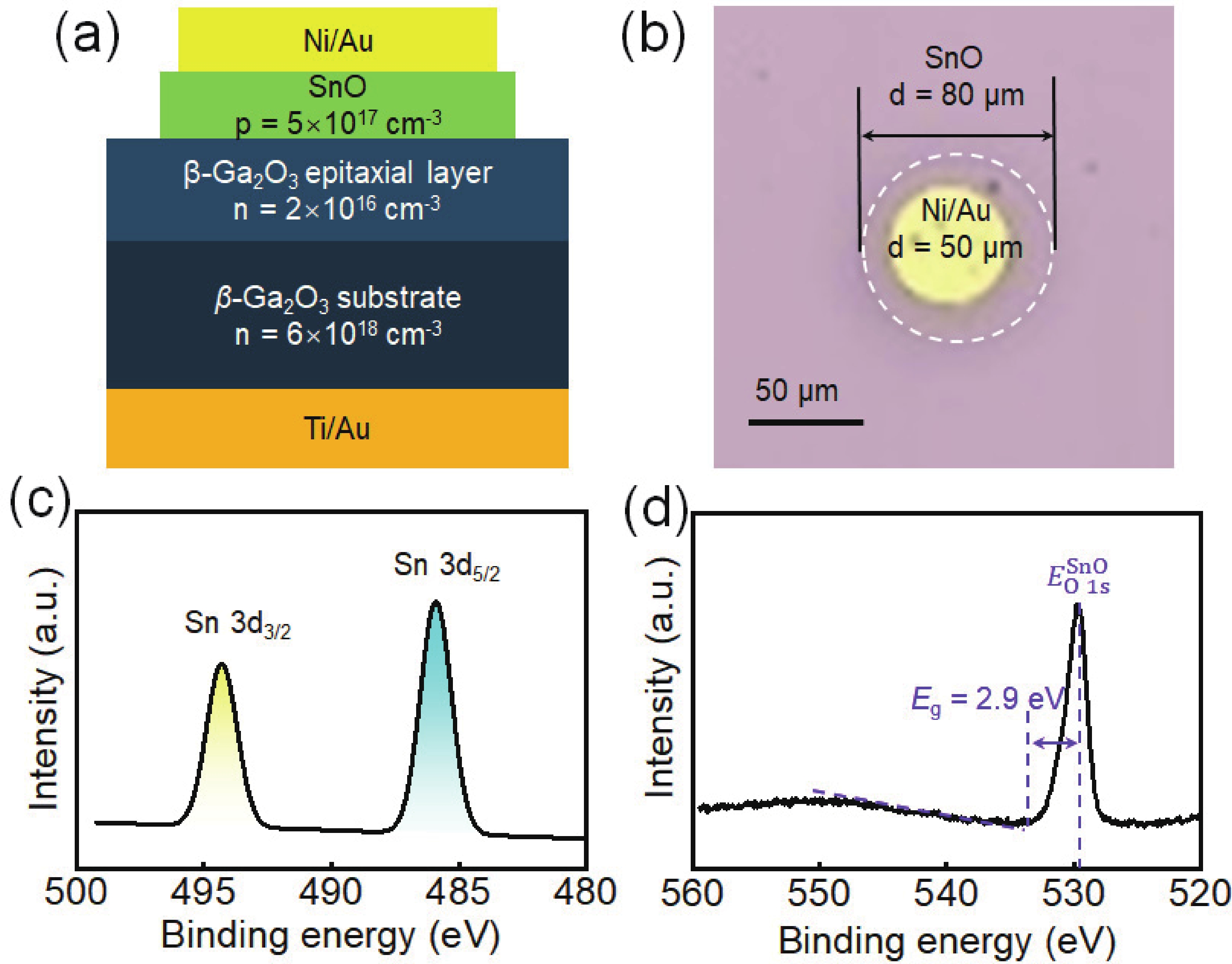
In this study, we present the fabrication of vertical SnO/β-Ga2O3 heterojunction diode (HJD) via radio frequency (RF) reactive magnetron sputtering. The valence and conduction band offsets between β-Ga2O3 and SnO are determined to be 2.65 and 0.75 eV, respectively, through X-ray photoelectron spectroscopy, showing a type-II band alignment. Compared to its Schottky barrier diode (SBD) counterpart, the HJD presents a comparable specific ON-resistances (Ron,sp) of 2.8 mΩ·cm² and lower reverse leakage current (IR), leading to an enhanced reverse blocking characteristics with breakdown voltage (BV) of 1675 V and power figure of merit (PFOM) of 1.0 GW/cm². This demonstrates the high quality of the SnO/β-Ga2O3 heterojunction interface. Silvaco TCAD simulation further reveals that electric field crowding at the edge of anode for the SBD was greatly depressed by the introduction of SnO film, revealing the potential application of SnO/β-Ga2O3 heterojunction in the future β-Ga2O3-based power devices.


The RADFET radiation dosimeter is a type of radiation detector based on the total dose effects of the PMOS transistor. The RADFET chip was fabricated in CUMEC 8-inch process with a six-layer photomask. The chip including two identical PMOS transistors, occupies a size of 610 µm×610 µm. Each PMOS has a W/L ratio of 300 µm/50 µm, and a 400 nm thick gate oxide, which is formed by a dry-wet-dry oxygen process. The wet oxygen-formed gate oxide with more traps can capture more holes during irradiation, thus significantly changing the PMOS threshold voltage. Pre-irradiation measurement results from ten test chips show that the initial average voltage of the PMOS is 1.961 V with a dispersion of 5.7%. The irradiation experiment is conducted in a cobalt source facility with a dose rate of 50 rad(Si)/s. During irradiation, a constant current source circuit of 10 µA was connected to monitoring the shift in threshold voltage under different total dose. When the total dose is 100 krad(Si), the shift in threshold voltage was approximately 1.37 V, which demonstrates that an excellent radiation function was achieved.


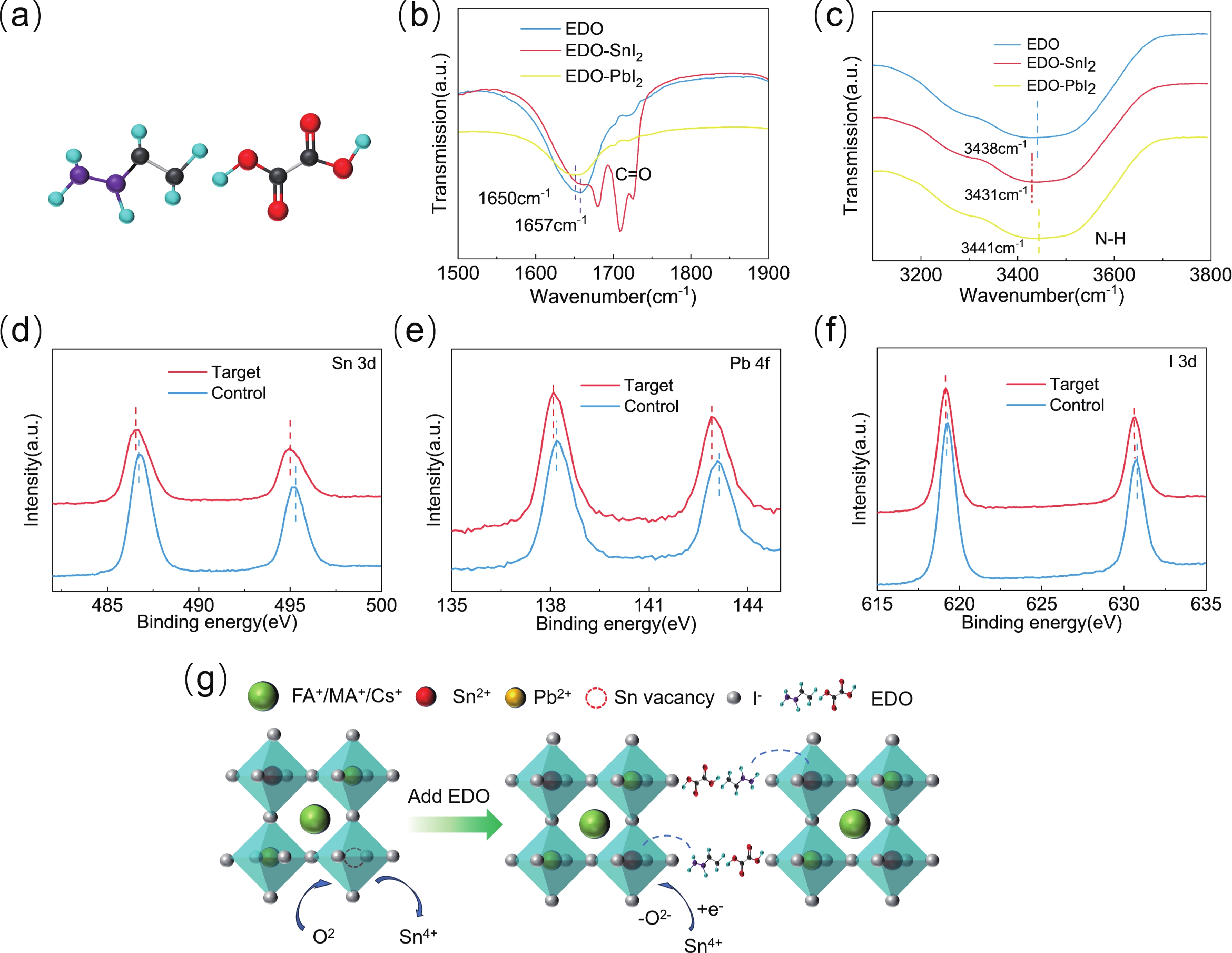
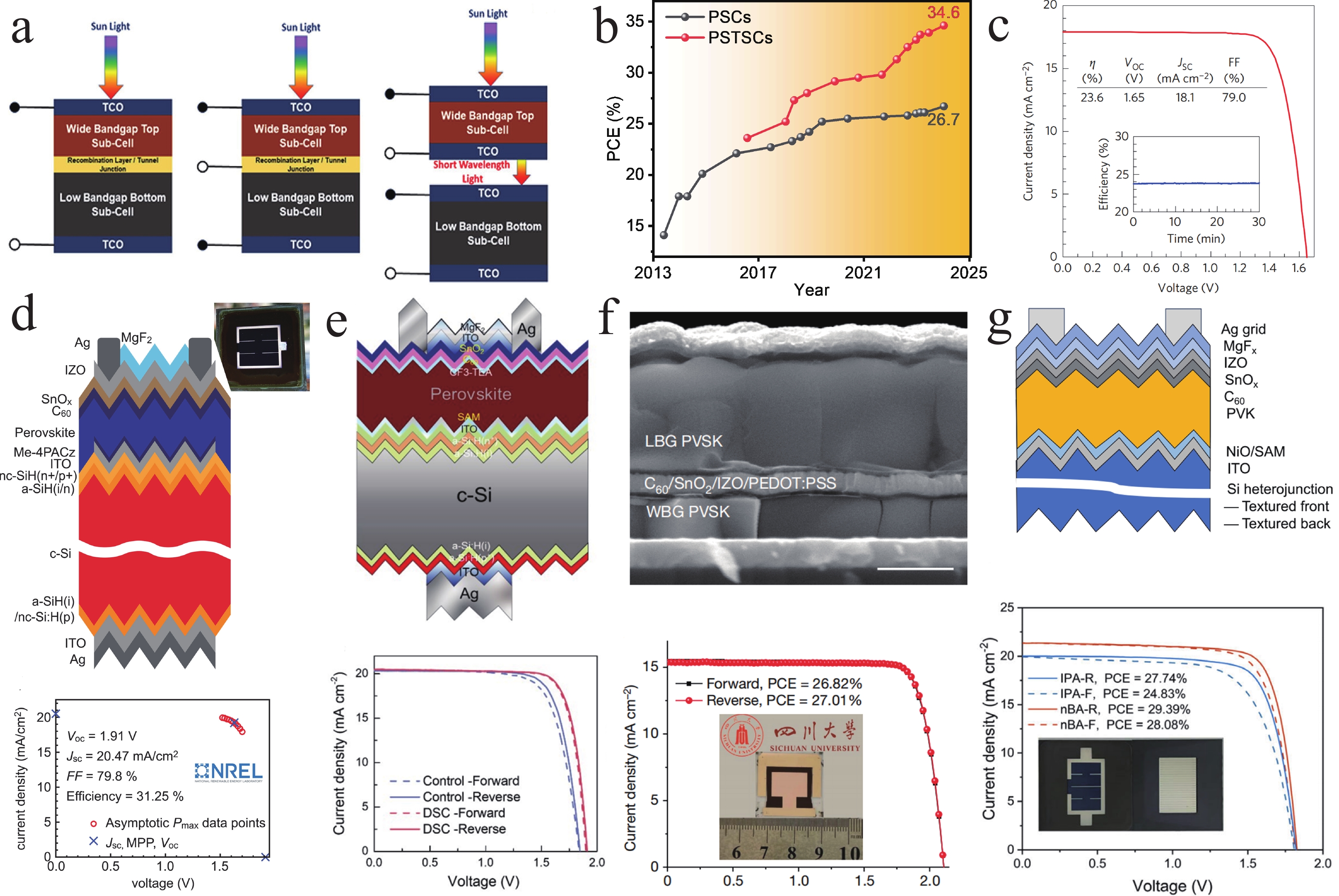
All-perovskite tandem solar cells (ATSCs) have the potential to surpass the Shockley−Queisser efficiency limit of conventional single-junction devices. However, the performance and stability of mixed tin–lead (Sn–Pb) perovskite solar cells (PSCs), which are crucial components of ATSCs, are much lower than those of lead-based perovskites. The primary challenges include the high crystallization rate of perovskite materials and the susceptibility of Sn2+ oxidation, which leads to rough morphology and unfavorable p-type self-doping. To address these issues, we introduced ethylhydrazine oxalate (EDO) at the perovskite interface, which effectively inhibits the oxidation of Sn2+ and simultaneously enhances the crystallinity of the perovskite. Consequently, the EDO-modified mixed tin−lead PSCs reached a power conversion efficiency (PCE) of 21.96% with high reproducibility. We further achieved a 27.58% efficient ATSCs by using EDO as interfacial passivator in the Sn−Pb PSCs.


Silicon carbide offers distinct advantages in the field of power electronic devices. However, manufacturing processes remain a significant barrier to its widespread adoption. Polycrystalline SiC is less expensive and easier to produce than single crystal. But stabilizing and controlling its performance are critical challenges that must be addressed urgently. Due to its material properties and excellent performance in applications, 3C-SiC is gaining increasing attention in research. This article presents the electrical and material properties of a series of polycrystalline 3C-SiC samples and investigates their interrelationship. The samples were examined using TEM, which confirmed their polycrystalline structure. Combined with XRD and Raman spectroscopy, the grain orientations within the samples were analyzed, and the presence of stress was verified. EBSD was employed to statistically examine the grain structure and size across samples. For samples with similar doping levels, grain size is the most influential factor in determining electrical characteristics. Further EBSD measurements reveal the relationship between resistivity and grain size as log(ρ) = −1.93 + 8.67/d. These findings provide a foundation for the quantitative control and application of polycrystalline 3C-SiC. This work offers theoretical evidence for optimizing the performance tuning of 3C-SiC ceramics and enhancing their effectiveness in electronic applications.


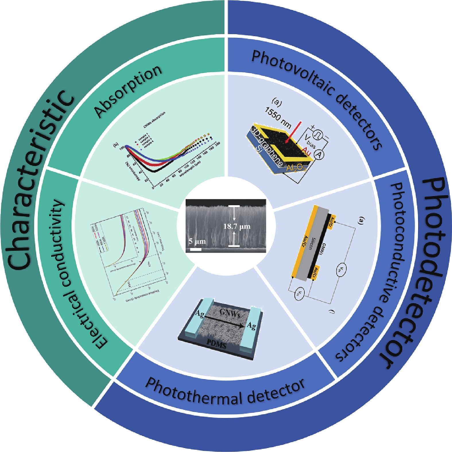
Graphene has garnered significant attention in photodetection due to its exceptional optical, electrical, mechanical, and thermal properties. However, the practical application of two-dimensional (2D) graphene in optoelectronic fields is limited by its weak light absorption (only 2.3%) and zero bandgap characteristics. Increasing light absorption is a critical scientific challenge for developing high-performance graphene-based photodetectors. Three-dimensional (3D) graphene comprises vertically grown stacked 2D-graphene layers and features a distinctive porous structure. Unlike 2D-graphene, 3D-graphene offers a larger specific surface area, improved electrochemical activity, and high chemical stability, making it a promising material for optoelectronic detection. Importantly, 3D-graphene has an optical microcavity structure that enhances light absorption through interaction with incoming light. This paper systematically reviews and analyzes the current research status and challenges of 3D-graphene-based photodetectors, aiming to explore feasible development paths for these devices and promote their industrial application.


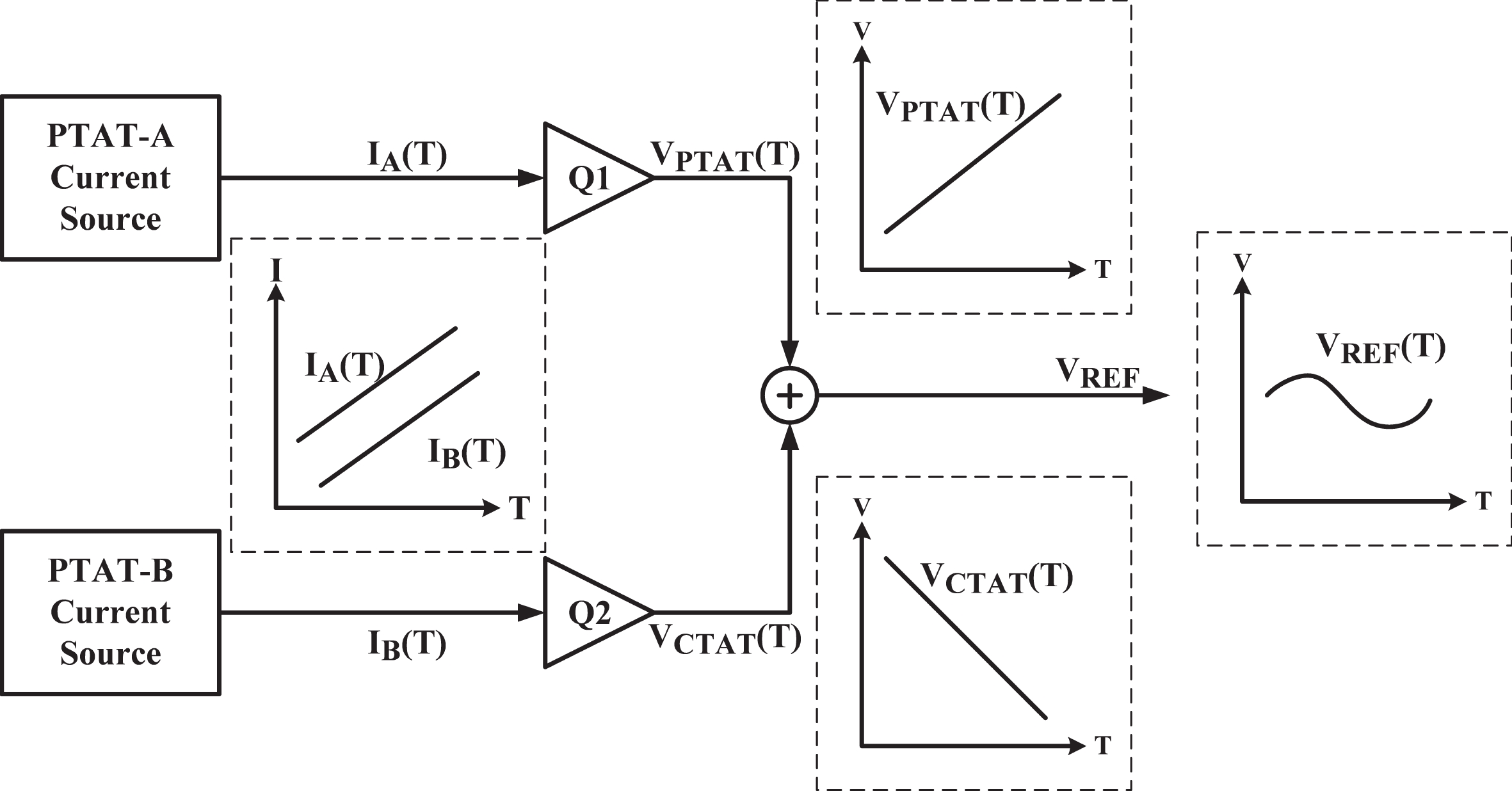
This brief presents a cryogenic voltage reference circuit designed to operate effectively across a wide temperature range from 30 to 300 K. A key feature of the proposed design is utilizing a current subtraction technique for temperature compensation of the reference current, avoiding the deployment of bipolar transistors to reduce area and power consumption. Implemented with a 0.18-µm CMOS process, the circuit achieves a temperature coefficient (TC) of 67.5 ppm/K, which was not achieved in previous works. The design can also attain a power supply rejection (PSR) of 58 dB at 10 kHz. Meanwhile, the average reference voltage is 1.2 V within a 1.6% 3σ-accuracy spread. Additionally, the design is characterized by a minimal power dissipation of 1 µW at 30 K and a compact chip area of 0.0035 mm².


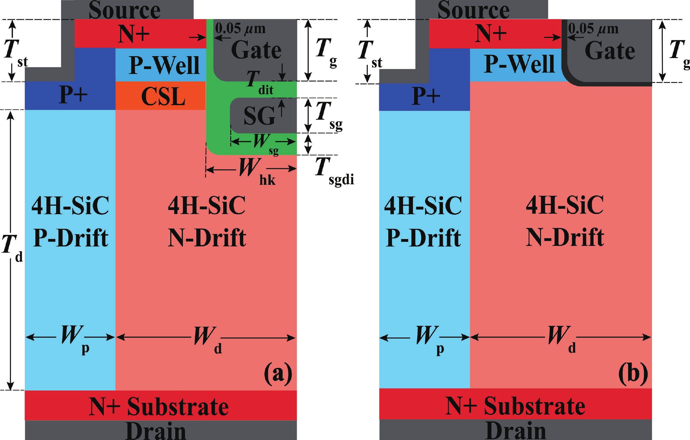
A 4H-SiC superjunction (SJ) MOSFET (SJMOS) with integrated high-K gate dielectric and split gate (HKSG−SJMOS) is proposed in this paper. The key features of HKSG−SJMOS involve the utilization of high-K (HK) dielectric as the gate dielectric, which surrounds the source-connected split gate (SG) and metal gate. The high-K gate dielectric optimizes the electric field distribution within the drift region, creating a low-resistance conductive channel. This enhancement leads to an increase in the breakdown voltage (BV) and a reduction in the specific on resistance (Ron,sp). The introduction of split gate surrounded by high-K dielectric reduces the gate−drain capacitance (Cgd) and gate−drain charge (Qgd), which improves the switching characteristics. The simulation results indicate that compared to conventional 4H-SiC SJMOS, the HKSG−SJMOS exhibits a 110.5% enhancement in figure of merit (FOM, FOM = BV2/Ron,sp), a 93.6% reduction in the high frequency figure of merit (HFFOM) of Ron,sp·Cgd, and reductions in turn-on loss (Eon) and turn-off loss (Eoff) by 38.3% and 31.6%, respectively. Furthermore, the reverse recovery characteristics of HKSG−SJMOS has also discussed, revealing superior performance compared to conventional 4H-SiC SJMOS.


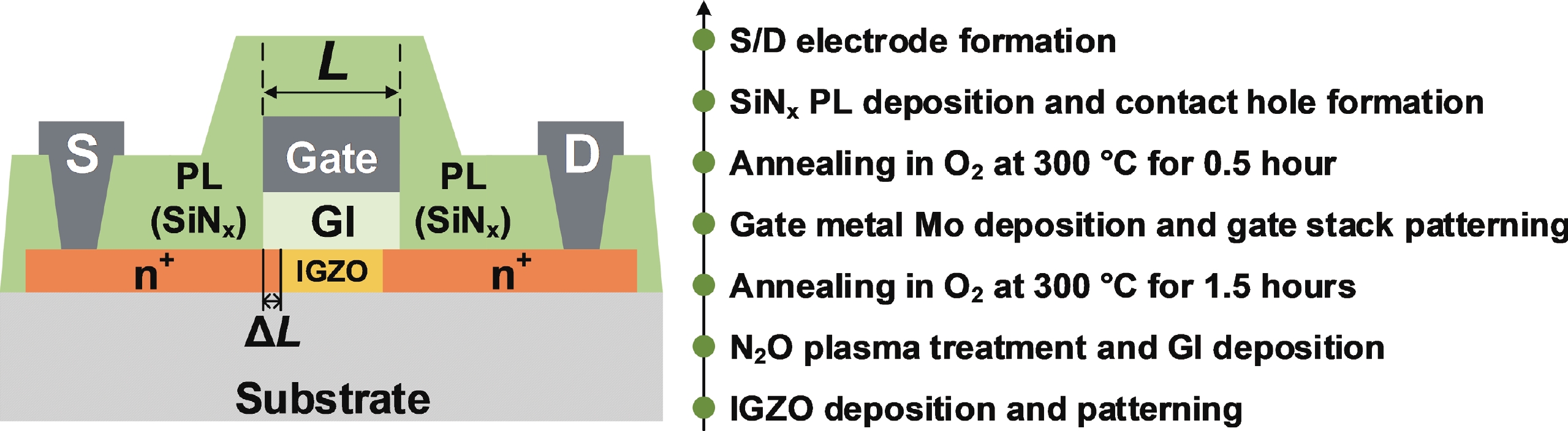
Besides the common short-channel effect (SCE) of threshold voltage (Vth) roll-off during the channel length (L) downscaling of InGaZnO (IGZO) thin-film transistors (TFTs), an opposite Vth roll-up was reported in this work. Both roll-off and roll-up effects of Vth were comparatively investigated on IGZO transistors with varied gate insulator (GI), source/drain (S/D), and device architecture. For IGZO transistors with thinner GI, the SCE was attenuated due to the enhanced gate controllability over the variation of channel carrier concentration, while the Vth roll-up became more noteworthy. The latter was found to depend on the relative ratio of S/D series resistance (RSD) over channel resistance (RCH), as verified on transistors with different S/D. Thus, an ideal S/D engineering with small RSD but weak dopant diffusion is highly expected during the downscaling of L and GI in IGZO transistors.


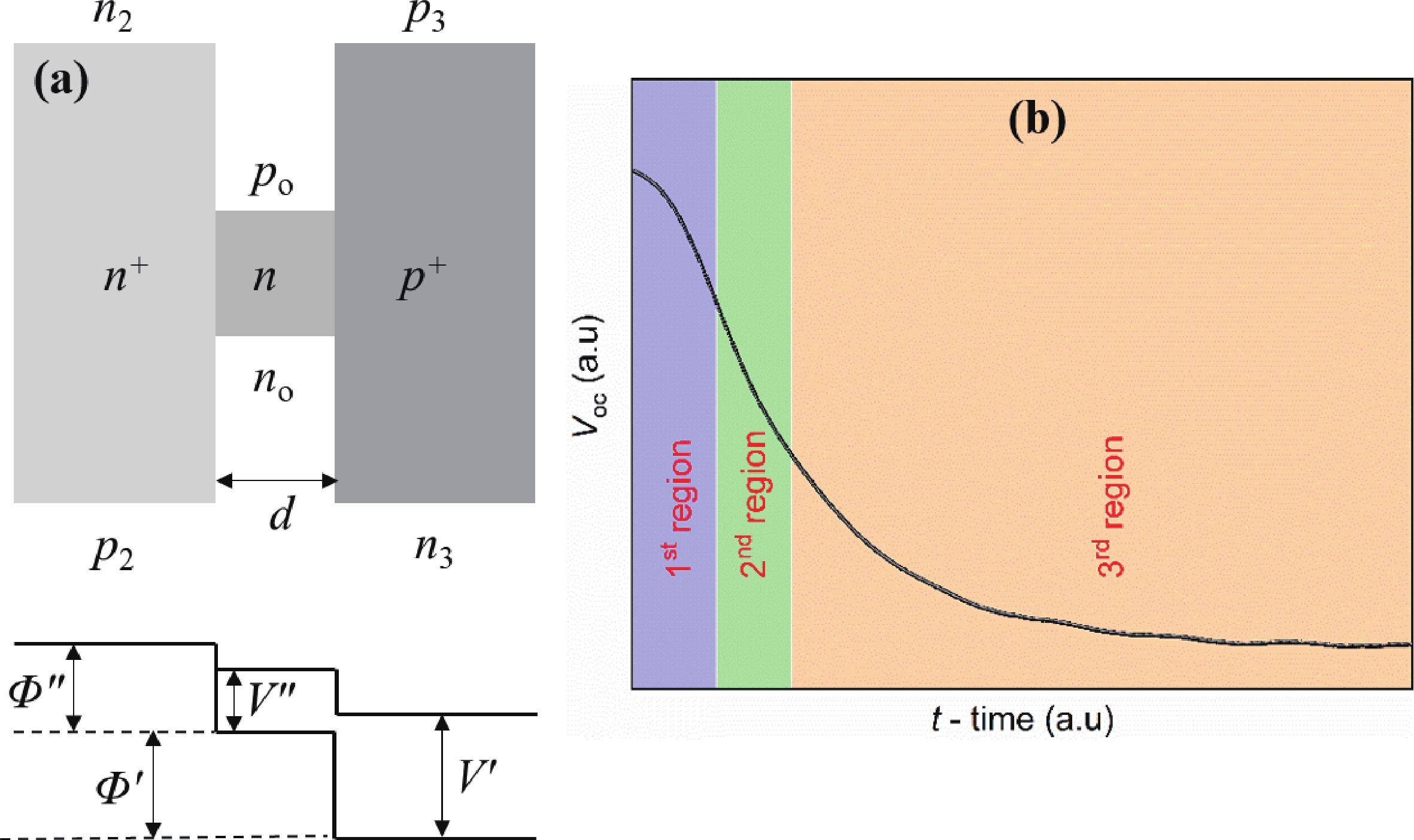
Minority carrier lifetimes τ are a fundamental parameter in semiconductor devices, representing the average time it takes for excess minority carriers to recombine. This characteristic is crucial for understanding and optimizing the performance of semiconductor materials, as it directly influences charge carrier dynamics and overall device efficiency. This work presents a development of PbS thin film deposited by thermal evaporation, at which the PbS thin film was further employed for structural, optical properties, and τ. Especially, the PbS film is probed with an in-house setup for identifying the τ. The procedure is to subject the PbS thin film with a flashlight from a light source with a middle rotating frequency. The derived τ in the in-house characterization setup agrees well with the value from the higher cost characterizing approach of photoluminescence. Therefore, the in-house setup provides additional tools for identifying the τ values for semiconductor devices.


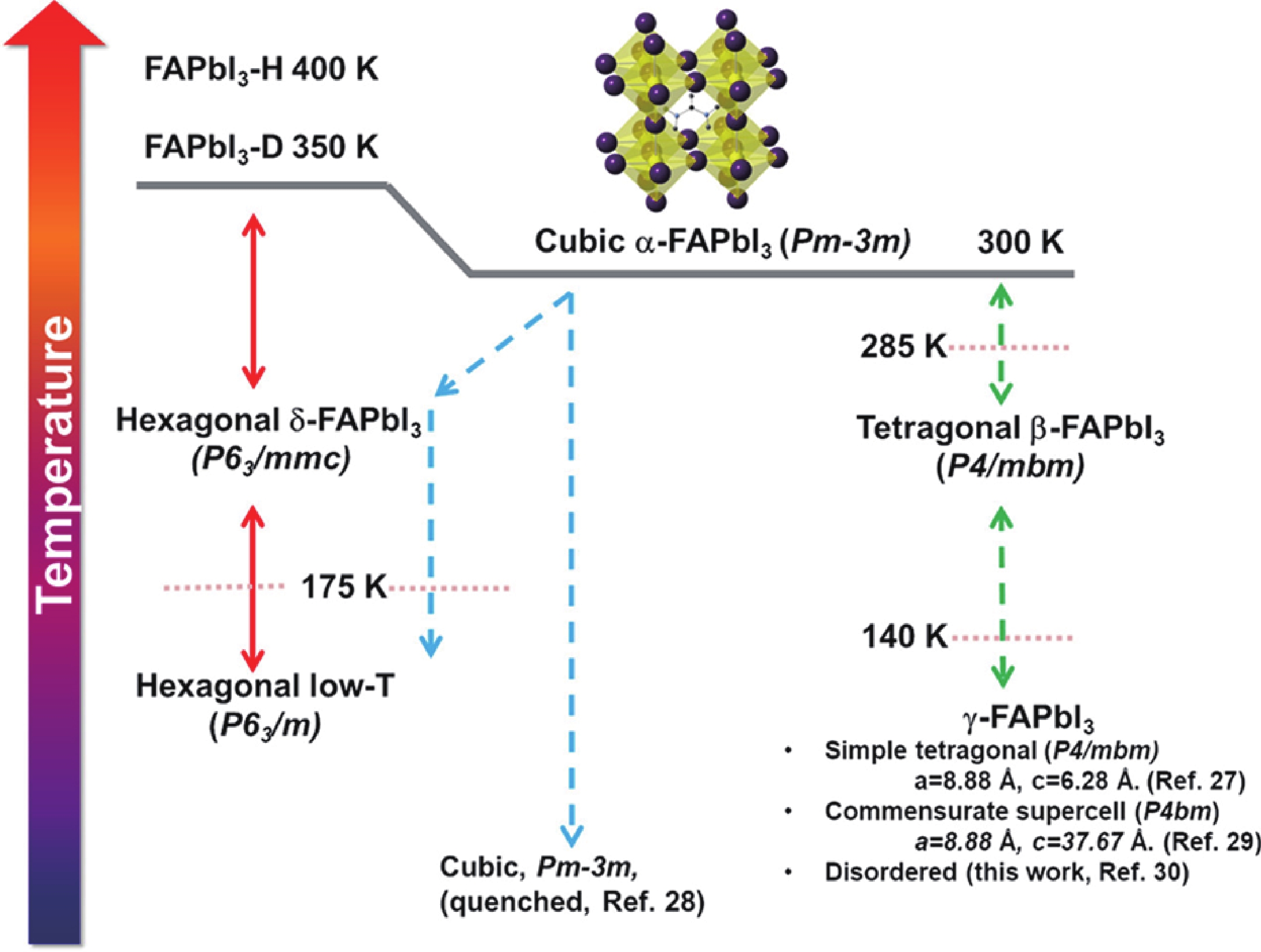
Halide perovskites have attracted great interest as active layers in optoelectronic devices. Among perovskites with diverse compositions, α-FAPbI3 is of utmost importance with great optoelectronic properties and a decent bandgap of 1.48 eV. However, the α-phase suffers an irreversible transition to the photo-inactive δ-phase, whereas the δ-phase is usually regarded as useless phase with poor optoelectronic properties. Therefore, it is commonly accepted that the thermodynamic stable δ-FAPbI3 greatly limits the application of FAPbI3. Every coin has two sides, although the δ-phase is difficult to apply as photoelectrical active layers, it is possible to combine δ-FAPbI3 with α-FAPbI3 to realize functional applications. Firstly, this review analyzes the cause of the contrasting properties between α- and δ-FAPbI3, where the stronger electron−phonon coupling in 1D hexagonal δ-FAPbI3 restricts its internal carrier and phonon transport. Secondly, the factors affecting the phase transitions and strategies to control phase transition between α- and δ-FAPbI3 are presented. Finally, some functional applications of δ-FAPbI3 in combination with α-FAPbI3 are given according to previous reports. By and large, we hope to introduce δ-FAPbI3 from another perspective and give some insights into its unique properties, hopefully providing new strategies for the subsequent advances to FAPbI3.


With the rapid advancement of 5G communication technology, increasingly stringent demands are placed on the performance and functionality of phase change switches. Given that RF and microwave signals exhibit characteristics of high frequency, high speed, and high precision, it is imperative for phase change switches to possess fast, accurate, and reliable switching capabilities. Moreover, wafer-level compositional homogeneity and resistivity uniformity during semiconductor manufacturing are crucial for ensuring the yield and reliability of RF switches. By controlling magnetron sputter of GeTe through from four key parameters (power, Ar flow, pressure, and post-annealing) and incorporating elemental proportional compensation in the target, we achieved effective modulation over GeTe uniformity. Finally, we successfully demonstrated the process integration of GeTe phase-change RF switches on 6-inch scaled wafers.


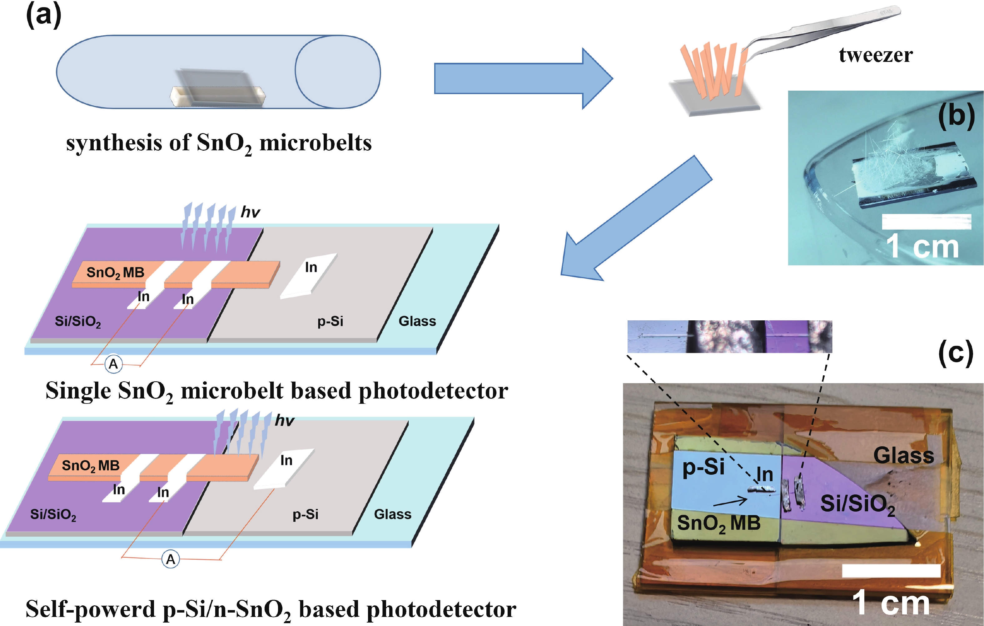
Recently, self-powered ultraviolet photodetectors (UV PDs) based on SnO2 have gained increasing interest due to its feature of working continuously without the need for external power sources. Nevertheless, the production of the majority of these existing UV PDs necessitates additional manufacturing stages or intricate processes. In this work, we present a facile, cost-effective approach for the fabrication of a self-powered UV PD based on p-Si/n-SnO2 junction. The self-powered device was achieved simply by integrating a p-Si substrate with a n-type SnO2 microbelt, which was synthesized via the chemical vapor deposition (CVD) method. The high-quality feature, coupled with the belt-like shape of the SnO2 microbelt enables the favorable contact between the n-type SnO2 and p-type silicon. The built-in electric field created at the interface endows the self-powered performance of the device. The p-Si/n-SnO2 junction photodetector demonstrated a high responsivity (0.12 mA/W), high light/dark current ratio (>103), and rapid response speed at zero bias. This method offers a practical way to develop cost-effective and high-performance self-powered UV PDs.


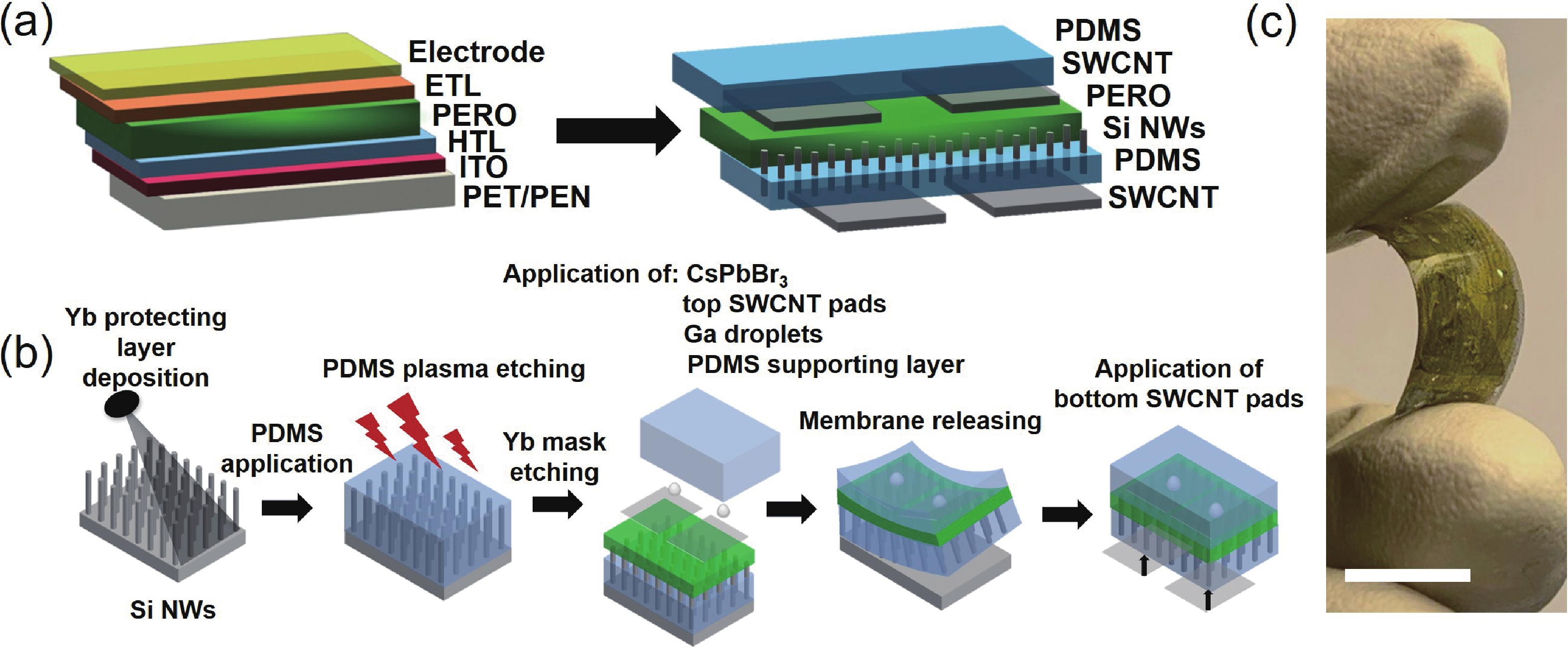
The emergence of cesium lead halide perovskite materials stable at air opened new prospects for the optoelectronic industry. In this work we present an approach to fabricating a flexible green perovskite light-emitting electrochemical cell (PeLEC) with a CsPbBr3 perovskite active layer using a highly-ordered silicon nanowire (Si NW) array as a distributed electrode integrated within a thin polydimethylsiloxane film (PDMS). Numerical simulations reveal that Si NWs-based distributed electrode aids the improvement of carrier injection into the perovskite layer with an increased thickness and, therefore, the enhancement of light-emitting performance. The X-ray diffraction study shows that the perovskite layer synthesized on the PDMS membrane with Si NWs has a similar crystal structure to the ones synthesized on planar Si wafers. We perform a comparative analysis of the light-emitting devices’ properties fabricated on rigid silicon substrates and flexible Si NW-based membranes released from substrates. Due to possible potential barriers in a flexible PeLEC between the bottom electrode (made of a network of single-walled carbon nanotube film) and Si NWs, the electroluminescence performance and I ̶ V properties of flexible devices deteriorated compared to rigid devices. The developed PeLECs pave the way for further development of inorganic flexible uniformly light-emitting devices with improved properties.


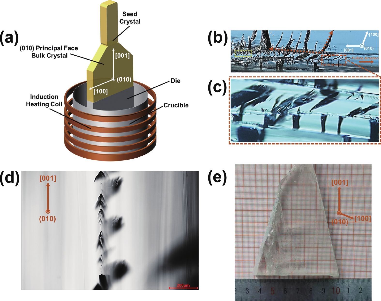
The (010)-oriented substrates of β-Ga2O3 are endowed with the maximum thermal conductivity and fastest homoepitaxial rate, which is the preferred substrate direction for high-power devices. However, the size of (010) plane wafer is critically limited by die in the commercial edge-defined film-fed growth (EFG) method. It is difficult to grow the β-Ga2O3 crystal with (010) principal face due to the (100) and (001) are cleavage planes. Here, the 2-inch diameter (010) principal-face β-Ga2O3 single crystal is successfully designed and grown by improved EFG method. Unlike previous reported techniques, the single crystals are pulled with [001] direction, and in this way the (010) wafers can be obtained from the principal face. In our experiments, tree-like defects (TLDs) in (010) principal-face bulk crystals are easy to generate. The relationship between stability of growth interface and origin of TLDs are thoroughly discussed. The TLDs are successfully eliminated by optimizing growth conditions. The high crystalline quality of (010)-oriented substrates are comprehensive demonstrated by full width at half maximum (FWHM) with 50.4 arcsec, consistent orientation arrangement of (010) plane, respectively. This work shows that the (010)-oriented substrates can be obtained by EFG method, predicting the commercial prospects of large-scale (010)-oriented β-Ga2O3 substrates.


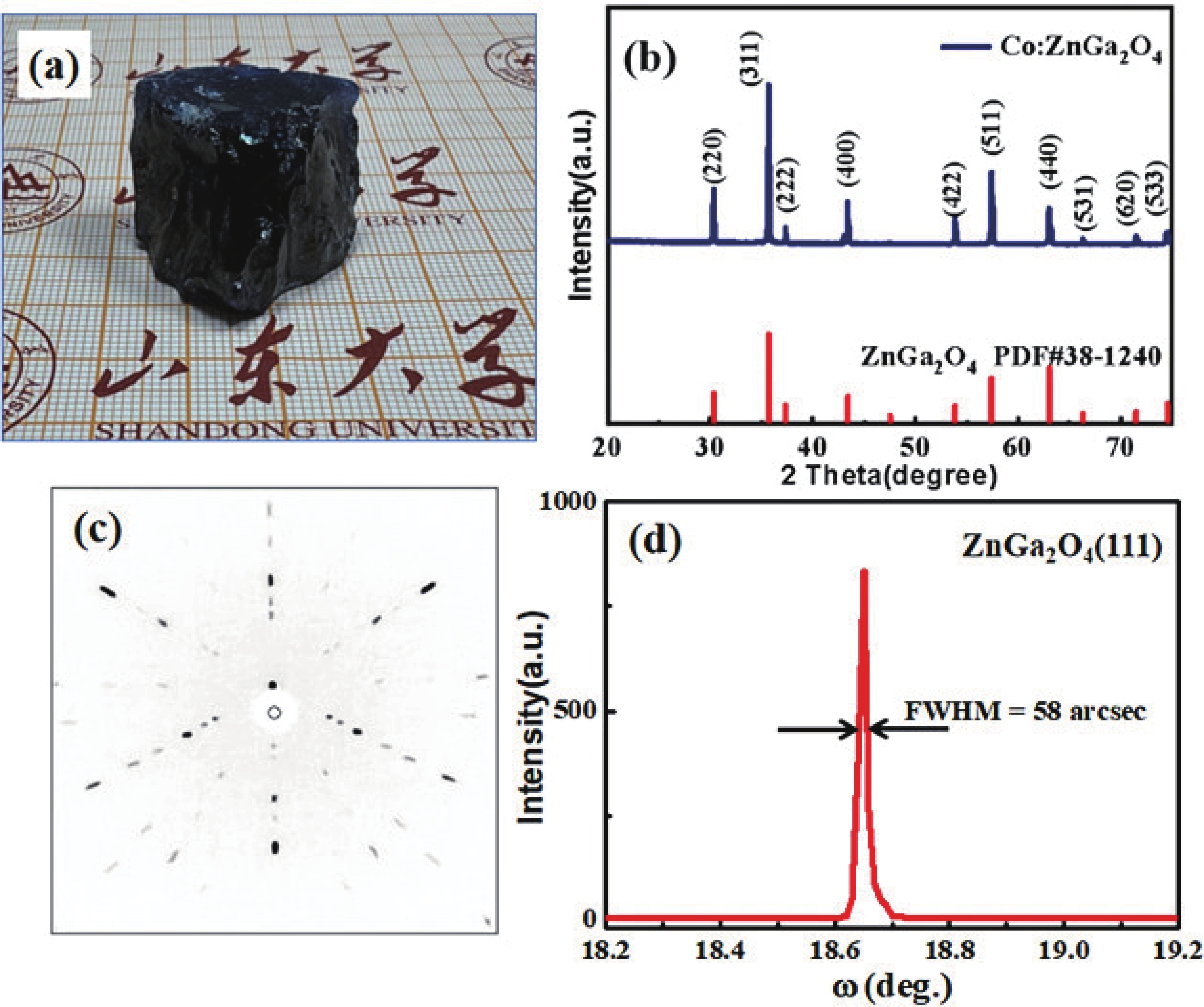
The transition of cobalt ions located at tetrahedral sites will produce strong absorption in the visible and near-infrared regions, and is expected to work in a passively Q-switched solid-state laser at the eye-safe wavelength of 1.5 µm. In this study, Co2+ ions were introduced into the wide bandgap semiconductor material ZnGa2O4, and large-sized and high-quality Co2+-doped ZnGa2O4 crystals with a volume of about 20 cm3 were grown using the vertical gradient freeze(VGF) method. Crystal structure and optical properties were analyzed using X-ray powder diffraction (XRD), X-ray photoelectron spectroscopy (XPS), and absorption spectroscopy. XRD results show that the Co2+-doped ZnGa2O4 crystal has a pure spinel phase without impurity phases and the rocking curve full width at half maximum (FWHM) is only 58 arcsec. The concentration of Co2+ in Co2+-doped ZnGa2O4 crystals was determined to be 0.2 at.% by the energy dispersive X-ray spectroscopy. The optical band gap of Co2+-doped ZnGa2O4 crystals is 4.44 eV. The optical absorption spectrum for Co2+-doped ZnGa2O4 reveals a prominent visible absorption band within 550−670 nm and a wide absorption band spanning from 1100 to 1700 nm. This suggests that the Co2+ ions have substituted the Zn2+ ions, which are typically tetrahedrally coordinated, within the lattice structure of ZnGa2O4. The visible region's absorption peak and the near-infrared broad absorption band are ascribed to the 4A2(4F) → 4T1(4P) and 4A2(4F) → 4T1(4F) transitions, respectively. The optimal ground state absorption cross section was determined to be 3.07 × 10⁻¹⁹ cm2 in ZnGa2O4, a value that is comparatively large within the context of similar materials. This finding suggests that ZnGa2O4 is a promising candidate for use in near-infrared passive Q-switched solid-state lasers.


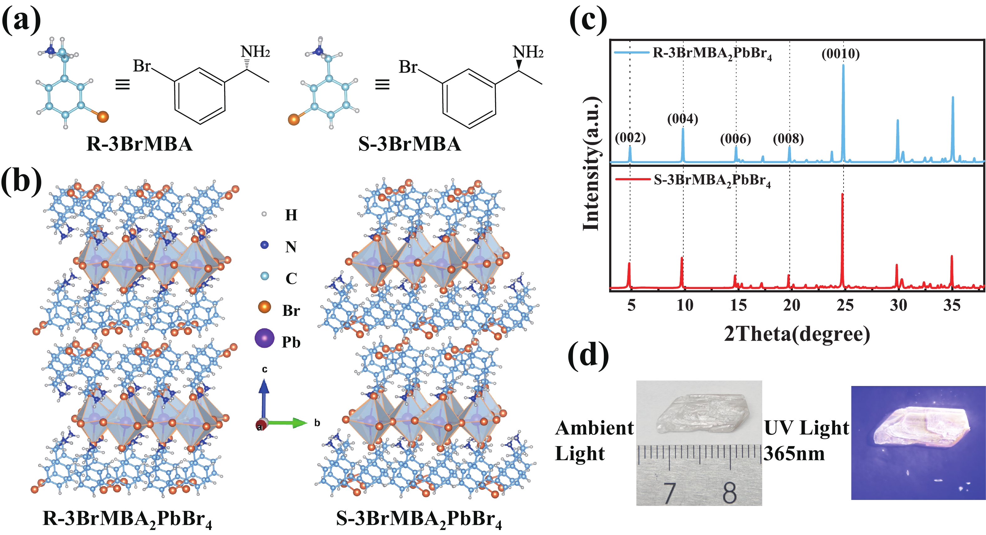
Two-dimensional (2D) chiral halide perovskites (CHPs) have attracted broad interest due to their distinct spin-dependent properties and promising applications in chiroptics and spintronics. Here, we report a new type of 2D CHP single crystals, namely R/S-3BrMBA2PbBr4. The chirality of the as-prepared samples is confirmed by exploiting circular dichroism spectroscopy, indicating a successful chirality transfer from chiral organic cations to their inorganic perovskite sublattices. Furthermore, we observed bright photoluminescence spanning from 380 to 750 nm in R/S-3BrMBA2PbBr4 crystals at room temperature. Such broad photoluminescence originates from free excitons and self-trapped excitons. In addition, efficient second-harmonic generation (SHG) performance was observed in chiral perovskite single crystals with high circular polarization ratios and non-linear optical circular dichroism. This demonstrates that R/S-3BrMBA2PbBr4 crystals can be used to detect and generate left- and right-handed circularly polarized light. Our study provides a new platform to develop high-performance chiroptical and spintronic devices.


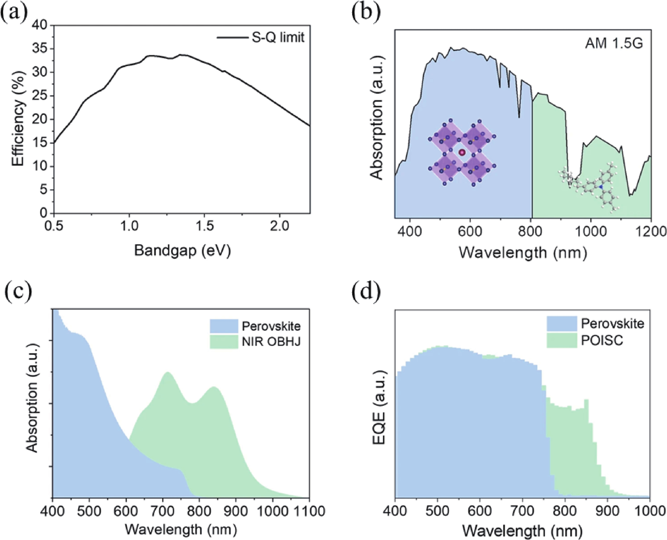
Integrated perovskite-organic solar cells (IPOSCs) offer a promising hybrid approach that combines the advantages of perovskite and organic solar cells, enabling efficient photon absorption across a broad spectrum with a simplified architecture. However, challenges such as limited charge mobility in organic bulk heterojunction (BHJ) layers, and energy-level mismatch at the perovskite/BHJ interface still sustain. Recent advancements in non-fullerene acceptors (NFAs), interfacial engineering, and emerging materials have improved charge transfer/transport, and overall power conversion efficiency (PCE) of IPOSCs. This review explores key developments in IPOSCs, focusing on low-bandgap materials for near-infrared absorption, energy alignment optimization, and strategies to enhance photocurrent density and device performance. Future innovations in material selection and device architecture will be crucial for further improving the efficiency of IPOSCs, bringing them closer to practical application in next-generation photovoltaic technologies.


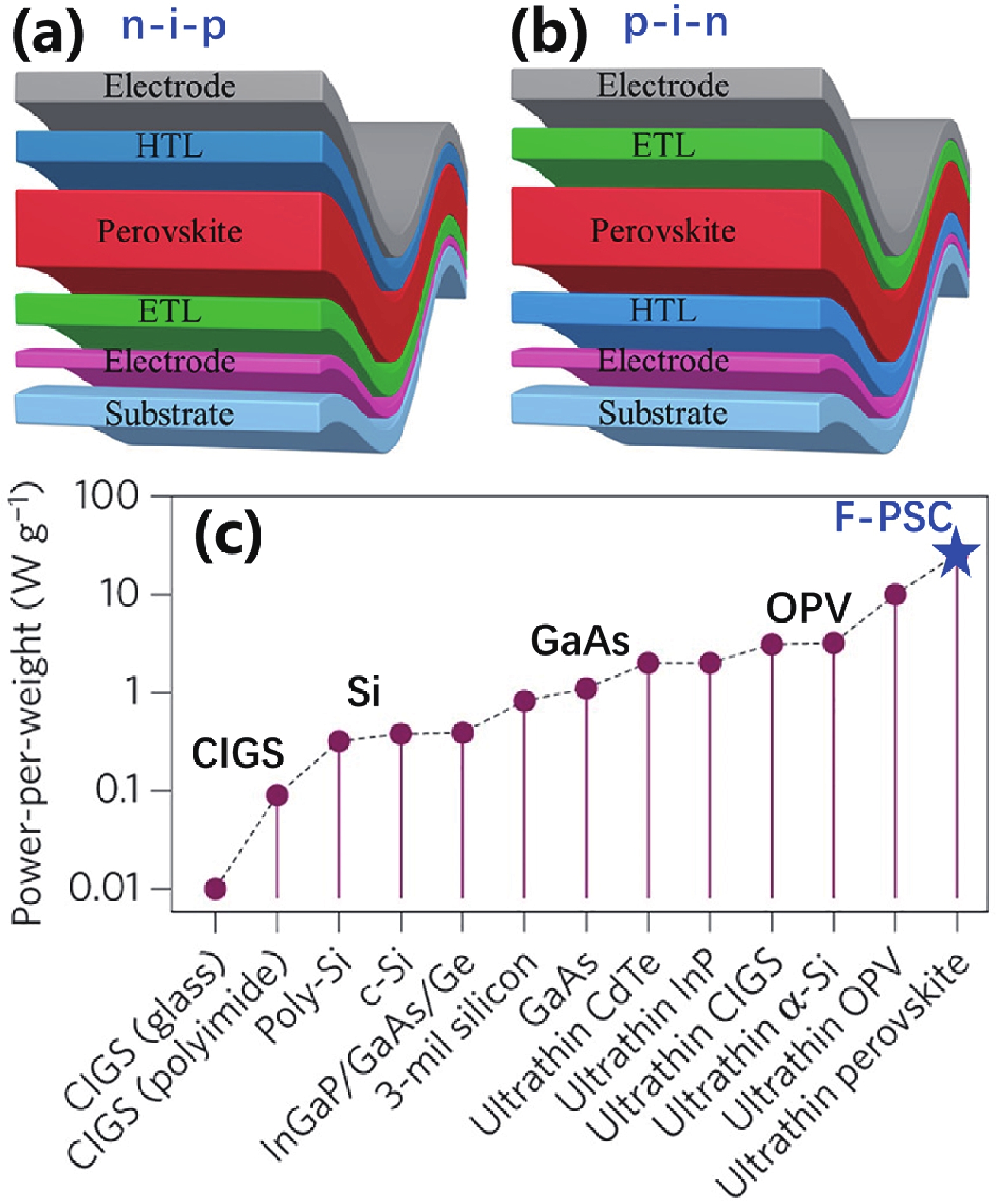
Due to advantages of high power-conversion efficiency (PCE), large power-to-weight ratio (PWR), low cost and solution processibility, flexible perovskite solar cells (f-PSCs) have attracted extensive attention in recent years. The PCE of f-PSCs has developed rapidly to over 25%, showing great application prospects in aerospace and wearable electronic devices. This review systematically sorts device structures and compositions of f-PSCs, summarizes various methods to improve its efficiency and stability recent years. In addition, the applications and potentials of f-PSCs in space vehicle and aircraft was discussed. At last, we prospect the key scientific and technological issues that need to be addressed for f-PSCs at current stage.


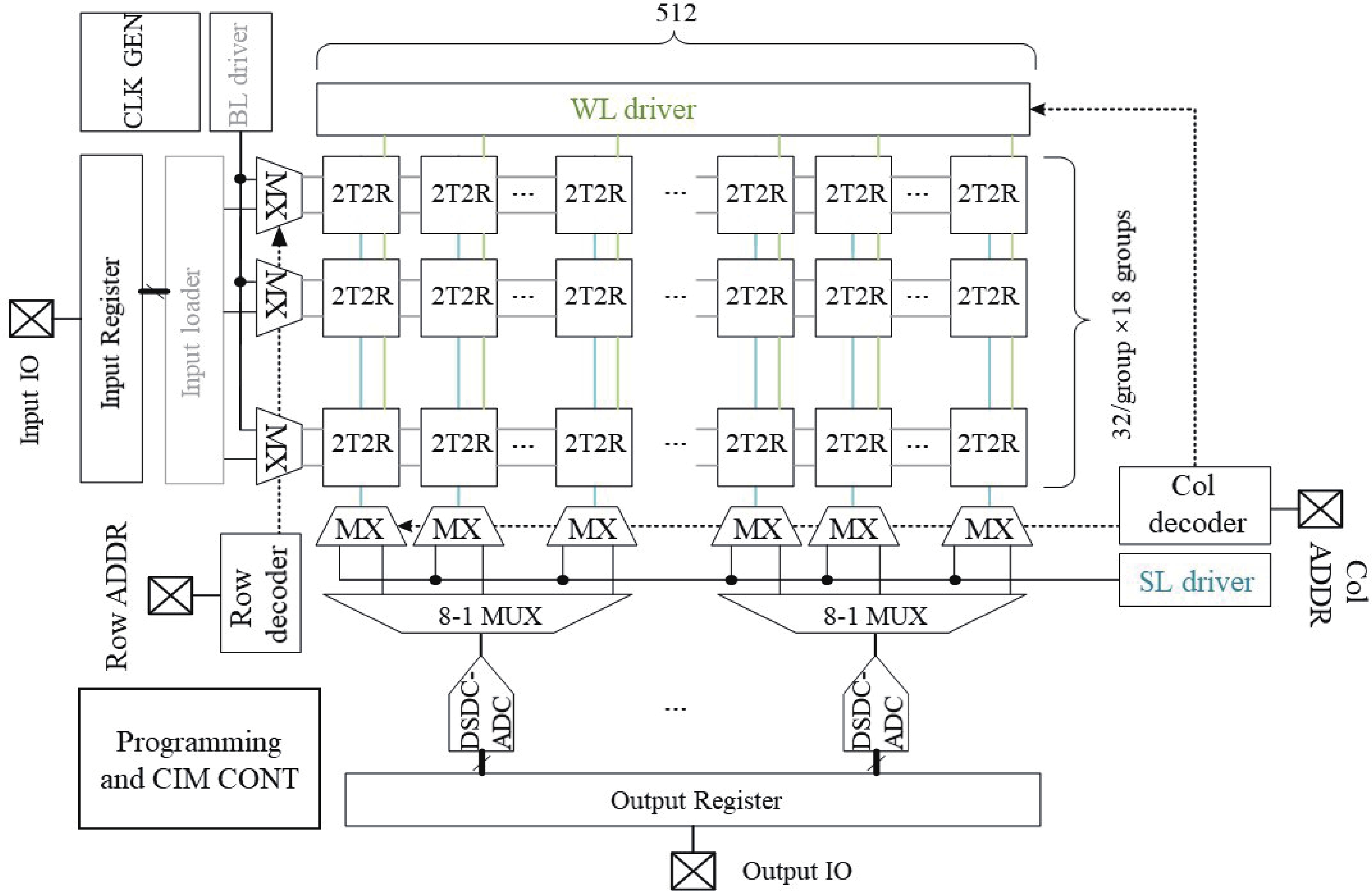
Computing-in-memory (CIM) has been a promising candidate for artificial-intelligent applications thanks to the absence of data transfer between computation and storage blocks. Resistive random access memory (RRAM) based CIM has the advantage of high computing density, non-volatility as well as high energy efficiency. However, previous CIM research has predominantly focused on realizing high energy efficiency and high area efficiency for inference, while little attention has been devoted to addressing the challenges of on-chip programming speed, power consumption, and accuracy. In this paper, a fabricated 28 nm 576K RRAM-based CIM macro featuring optimized on-chip programming schemes is proposed to address the issues mentioned above. Different strategies of mapping weights to RRAM arrays are compared, and a novel direct-current ADC design is designed for both programming and inference stages. Utilizing the optimized hybrid programming scheme, 4.67× programming speed, 0.15× power saving and 4.31× compact weight distribution are realized. Besides, this macro achieves a normalized area efficiency of 2.82 TOPS/mm2 and a normalized energy efficiency of 35.6 TOPS/W.


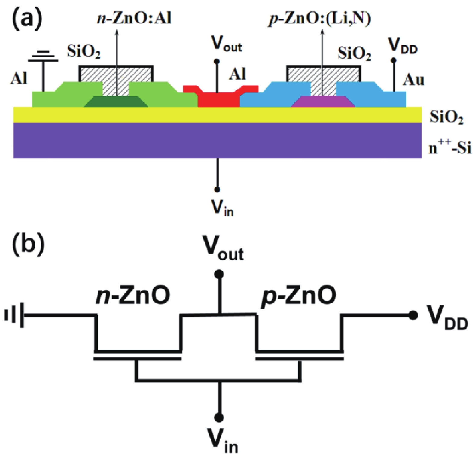
Complementary inverter is the basic unit for logic circuits, but the inverters based on full oxide thin-film transistors (TFTs) are still very limited. The next challenge is to realize complementary inverters using homogeneous oxide semiconductors. Herein, we propose the design of complementary inverter based on full ZnO TFTs. Li−N dual-doped ZnO (ZnO:(Li,N)) acts as the p-type channel and Al-doped ZnO (ZnO:Al) serves as the n-type channel for fabrication of TFTs, and then the complementary inverter is produced with p- and n-type ZnO TFTs. The homogeneous ZnO-based complementary inverter has typical voltage transfer characteristics with the voltage gain of 13.34 at the supply voltage of 40 V. This work may open the door for the development of oxide complementary inverters for logic circuits.


As a type of charge-balanced power device, the performance of super-junction MOSFETs (SJ-MOS) is significantly influenced by fluctuations in the fabrication process. To overcome the relatively narrow process window of conventional SJ-MOS, an optimized structure "vertical variable doping super-junction MOSFET (VVD-SJ)" is proposed. Based on the analysis using the charge superposition principle, it is observed that the VVD-SJ, in which the impurity concentration of the P-pillar gradually decreases while that of the N-pillar increases from top to bottom, improves the electric field distribution and mitigates charge imbalance (CIB). Experimental results demonstrate that the optimized 600 V VVD-SJ achieves a 35.90% expansion of the process window.


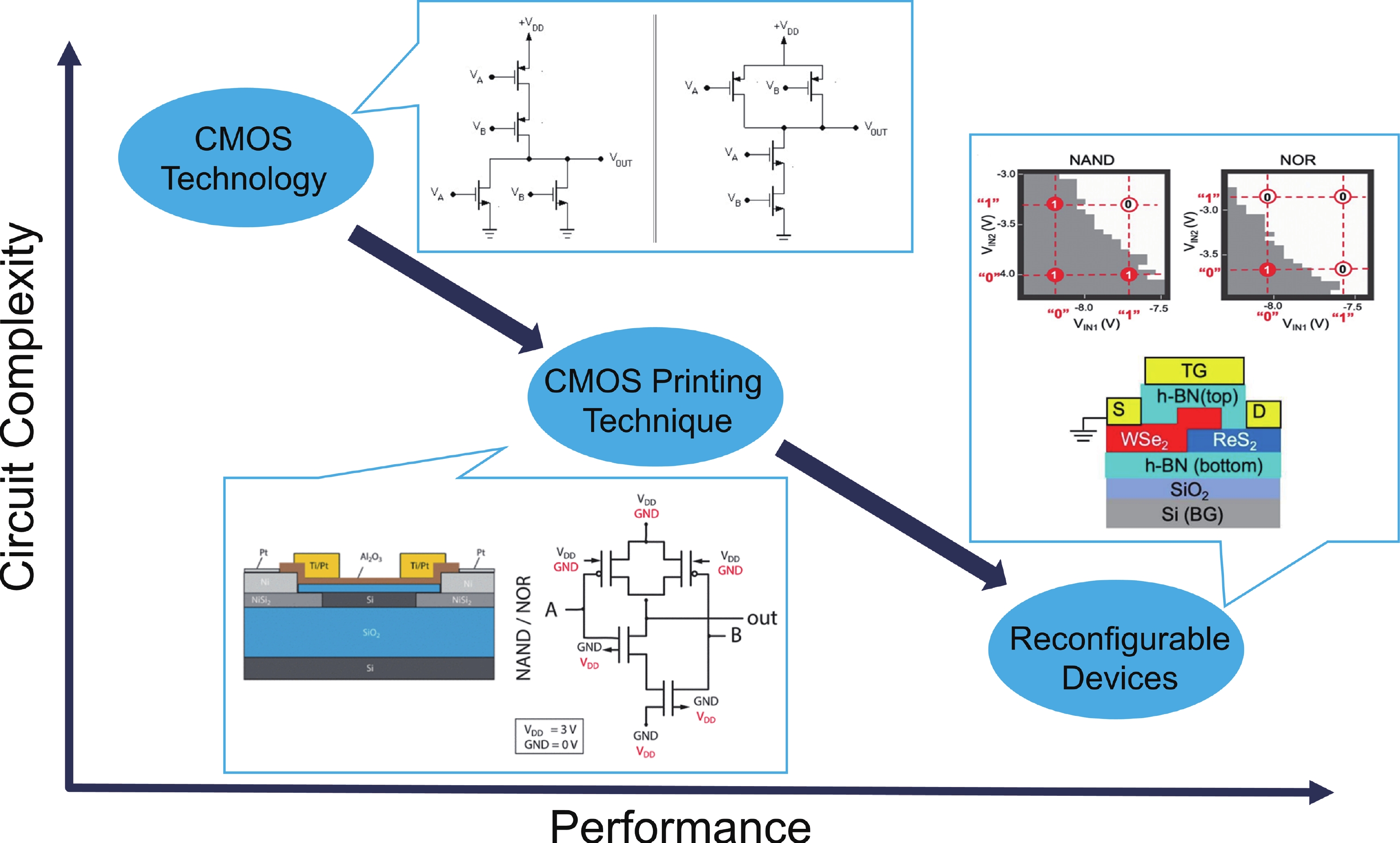
In recent years, as the dimensions of the conventional semiconductor technology is approaching the physical limits, while the multifunction circuits are restricted by the relatively fixed characteristics of the traditional metal−oxide−semiconductor field-effect transistors, reconfigurable devices that can realize reconfigurable characteristics and multiple functions at device level have been seen as a promising method to improve integration density and reduce power consumption. Owing to the ultrathin structure, effective control of the electronic characteristics and ability to modulate structural defects, two-dimensional (2D) materials have been widely used to fabricate reconfigurable devices. In this review, we summarize the working principles and related logic applications of reconfigurable devices based on 2D materials, including generating tunable anti-ambipolar responses and demonstrating nonvolatile operations. Furthermore, we discuss the analog signal processing applications of anti-ambipolar transistors and the artificial intelligence hardware implementations based on reconfigurable transistors and memristors, respectively, therefore highlighting the outstanding advantages of reconfigurable devices in footprint, energy consumption and performance. Finally, we discuss the challenges of the 2D materials-based reconfigurable devices.


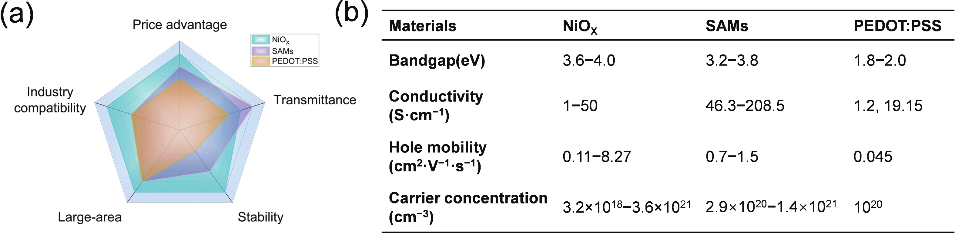
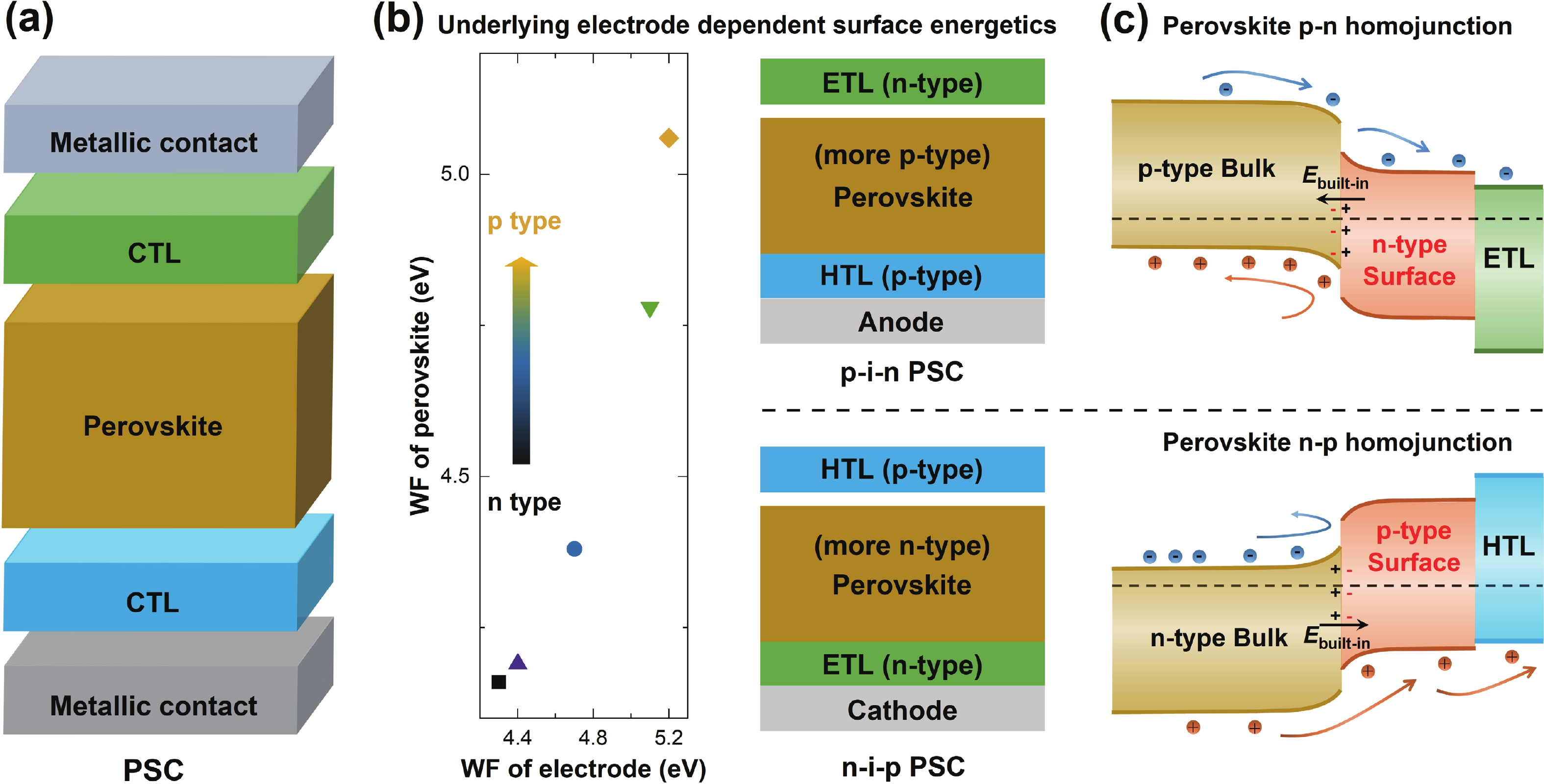
Perovskite solar cells (PSCs) have become a hot topic in the field of renewable energy due to their excellent power conversion efficiency and potential for low-cost manufacturing. The hole transport layer (HTL), as a key component of PSCs, plays a crucial role in the cell's overall performance. Magnetron sputtering NiOx has attracted widespread attention due to its high carrier mobility, excellent stability, and suitability for large-scale production. Herein, an insightful summary of the recent progress of magnetron sputtering NiOx as the HTL of PSCs is presented to promote its further development. This review summarized the basic properties of magnetron sputtering NiOx thin film, the key parameters affecting the optoelectronic properties of NiOx thin films during the magnetron-sputtering process, and the performance of the corresponding PSCs. Special attention was paid to the interfacial issues between NiOx and perovskites, and the modification strategies were systematically summarized. Finally, the challenges of sputtering NiOx technology and the possible development opportunities were concluded and discussed.


