


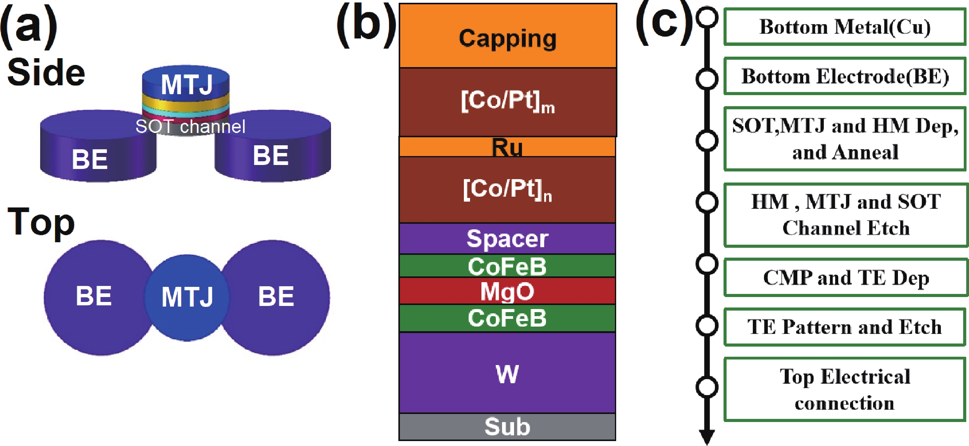
Fig. 1.
(Color online) (a) Top and side view of the novel designed SOT-MTJ device structure. (b) Schematic of the TP MTJ stack. (c) Main steps of Integration process.
ARTICLES
Zhenghui Ji, Guoxiu Qiu, Qijun Guo, Enlong Liu, Wenlong Yang, Qingxiu Li, Lei Zhao, Hengan Zhou, Dinggui Zeng, Shasha Wang, Weiming He and ShiKun He
Corresponding author: ShiKun He, Email: he_shikun@hikstor.com
Abstract: The mechanism of the etching process that ensures high yield in spin-orbit torque magnetic random-access memory (SOT-MRAM) featuring a novel channel-less (CHL) structure is systematically investigated in this paper. A steep sidewall morphology is identified as particularly favorable, and the precise relationship between the pillar profile and yield is established and thoroughly analyzed. When the step angle exceeds 80°, a larger net etching rate along the sidewall is achieved, enabling effective removal of metal residues near the tunnel barrier layer while minimizing plasma-induced damage at the MgO/CoFeB interface. The optimized devices exhibit an excellent thermal stability factor (Δ) of over 95 at room temperature, demonstrating superior operational reliability. Thanks to process optimizations targeting re-deposition removal, the in-die functional yield of the fabricated 16 Kb CHL SOT-MRAM array reaches an impressive 60 ppm. These advancements pave the way for high-yield and reliable mass production of SOT-MRAM devices.
Keywords: channel-less SOT-MRAM, Ion beam etch, High yield, 300 mm wafer platform
| [1] |
Ikeda S, Miura K, Yamamoto H, et al. A perpendicular-anisotropy CoFeB–MgO magnetic tunnel junction. Nature Mater, 2010, 9(9): 721. doi: 10.1038/nmat2804
|
| [2] |
Watanabe K, Jinnai B, Fukami S, et al. Shape anisotropy revisited in single-digit nanometer magnetic tunnel junctions. Nat Commun, 2018, 9: 663. doi: 10.1038/s41467-018-03003-7
|
| [3] |
Khvalkovskiy A V, Apalkov D, Watts S, et al. Basic principles of STT-MRAM cell operation in memory arrays. J Phys D: Appl Phys, 2013, 46(7): 074001. doi: 10.1088/0022-3727/46/7/074001
|
| [4] |
Carboni R, Ambrogio S, Chen W, et al. Understanding cycling endurance in perpendicular spin-transfer torque (p-STT) magnetic memory. 2016 IEEE International Electron Devices Meeting (IEDM), 2017: 21.6. 1.
|
| [5] |
Garello K, Yasin F, Couet S, et al. SOT-MRAM 300MM integration for low power and ultrafast embedded memories. 2018 IEEE Symposium on VLSI Circuits, 2018: 81.
|
| [6] |
Van Beek S, Cai K, Yasin F, et al. Scaling the SOT track–A path towards maximizing efficiency in SOT-MRAM. 2023 International Electron Devices Meeting (IEDM), 2023: 1.
|
| [7] |
Chen G L, Wang I J, Yeh P S, et al. An 8kb spin-orbit-torque magnetic random-access memory. 2021 International Symposium on VLSI Technology, Systems and Applications (VLSI-TSA), 2021: 1.
|
| [8] |
Y X Yao, S Y Cheng, S Y Lu, et al. Double CoFeB reference layers for optimized PMA and BEOL compatibility of SOT-MRAM. J. Semicond. , 2026, accepted, https://doi.org/ 10.1088/1674-4926/26010048.
|
| [9] |
Nguyen V D, Rao S, Wostyn K, et al. Recent progress in spin-orbit torque magnetic random access memory. npj Spintron, 2024, 2: 48. doi: 10.1038/s44306-024-00044-1
|
| [10] |
Zhang H C, Ma X Y, Jiang C P, et al. Integration of high-performance spin-orbit torque MRAM devices by 200-mm-wafer manufacturing platform. J Semicond, 2022, 43(10): 102501. doi: 10.1088/1674-4926/43/10/102501
|
| [11] |
Jiang C P, Li J H, Zhang H C, et al. Demonstration of a manufacturable SOT-MRAM multiplexer array towards industrial applications. J Semicond, 2023, 44(12): 122501. doi: 10.1088/1674-4926/44/12/122501
|
| [12] |
Sato N, Allen G A, Benson W P, et al. CMOS compatible process integration of SOT-MRAM with heavy-metal bi-layer bottom electrode and 10ns field-free SOT switching with STT assist. 2020 IEEE Symposium on VLSI Technology, 2020: 1.
|
| [13] |
Zhao L, Yang M Y, Gao J F, et al. Enhancement of magnetic and electric transport performance of perpendicular spin-orbit torque magnetic tunnel junction by stop-on-MgO etching process. IEEE Electron Device Lett, 2023, 44(3): 408. doi: 10.1109/LED.2023.3236835
|
| [14] |
Yang W L, Ji Z H, Gao Y, et al. Achieving high yield of perpendicular SOT-MTJ manufactured on 300 mm wafers. IEEE Electron Device Lett, 2024, 45(11): 2094. doi: 10.1109/led.2024.3454609
|
| [15] |
Liu E L, Yang W L, Zhou K Y, et al. A novel channel-less SOT-MRAM with 115% TMR, 2 ns switching, and high bit yield (>99.9%). 2024 IEEE International Electron Devices Meeting (IEDM), 2025: 1.
|
| [16] |
Miron I M, Garello K, Gaudin G, et al. Perpendicular switching of a single ferromagnetic layer induced by in-plane current injection. Nature, 2011, 476(7359): 189. doi: 10.1038/nature10309
|
| [17] |
Liu L Q, Lee O J, Gudmundsen T J, et al. Current-induced switching of perpendicularly magnetized magnetic layers using spin torque from the spin Hall effect. Phys Rev Lett, 2012, 109(9): 096602. doi: 10.1103/PhysRevLett.109.096602
|
| [18] |
Liu L Q, Pai C-F, Li Y, et al. Spin-torque switching with the giant spin Hall effect of tantalum. Science, 2012, 336(6081): 555. doi: 10.1126/science.1218197
|
| [19] |
Jeong J, Endoh T. Ion beam etching process for high-density spintronic devices and its damage recovery by the oxygen showering post-treatment process. Jpn J Appl Phys, 2017, 56(4S): 04CE09. doi: 10.7567/JJAP.56.04CE09
|
| [20] |
Gokan H, Esho S. Pattern fabrication by oblique incidence ion-beam etching. J Vac Sci Technol, 1981, 18(1): 23. doi: 10.1116/1.570693
|
| [21] |
Takahashi S, Kai T, Shimomura N, et al. Ion-beam-etched profile control of MTJ cells for improving the switching characteristics of high-density MRAM. IEEE Trans Magn, 2006, 42(10): 2745. doi: 10.1109/TMAG.2006.878862
|
| [22] |
Islam R, et al. Dry etching strategy of spin-transfer-torque magnetic random access memory: A review. J Vac Sci Technol B, 2020, 38(5): 050801. doi: 10.1116/6.0000205
|
| [23] |
Thomas L, Jan G, Le S, et al. Solving the paradox of the inconsistent size dependence of thermal stability at device and chip-level in perpendicular STT-MRAM. 2015 IEEE International Electron Devices Meeting (IEDM), 2016: 26.4. 1.
|
| [24] |
Yan Z R, Lu P Q, Chu Y Y, et al. Magnetic-field orientation dependence of thermal stability in perpendicular STT-MRAM. IEEE Electron Device Lett, 2025, 46(2): 191. doi: 10.1109/LED.2024.3513954
|
| [25] |
Cui J-L, Shi T X, Wang S Y, et al. A 492.8-TOPS/W STT-MRAM sparsity-adaptive compute-in-memory macro for edge AI inference. IEEE J Solid State Circuits, 2026: 1.
|
| [26] |
Fang Z H, Zhu H J, Du H R, et al. Elaborated dual-path SOT-MRAM achieving 500-MHz read and 100-MHz write for energy-constraint applications. IEEE Trans Circuits Syst I Regul Pap, 2026, 73(4): 2546. doi: 10.1109/TCSI.2025.3631103
|
| [27] |
Ko S, Shim J, Park J H, et al. Key technologies of scaling embedded MRAM to 8nm logic and beyond for automotive application. 2024 IEEE International Electron Devices Meeting (IEDM). San Francisco, CA, USA. IEEE, 2025: 1.
|

| [1] |
Ikeda S, Miura K, Yamamoto H, et al. A perpendicular-anisotropy CoFeB–MgO magnetic tunnel junction. Nature Mater, 2010, 9(9): 721. doi: 10.1038/nmat2804
|
| [2] |
Watanabe K, Jinnai B, Fukami S, et al. Shape anisotropy revisited in single-digit nanometer magnetic tunnel junctions. Nat Commun, 2018, 9: 663. doi: 10.1038/s41467-018-03003-7
|
| [3] |
Khvalkovskiy A V, Apalkov D, Watts S, et al. Basic principles of STT-MRAM cell operation in memory arrays. J Phys D: Appl Phys, 2013, 46(7): 074001. doi: 10.1088/0022-3727/46/7/074001
|
| [4] |
Carboni R, Ambrogio S, Chen W, et al. Understanding cycling endurance in perpendicular spin-transfer torque (p-STT) magnetic memory. 2016 IEEE International Electron Devices Meeting (IEDM), 2017: 21.6. 1.
|
| [5] |
Garello K, Yasin F, Couet S, et al. SOT-MRAM 300MM integration for low power and ultrafast embedded memories. 2018 IEEE Symposium on VLSI Circuits, 2018: 81.
|
| [6] |
Van Beek S, Cai K, Yasin F, et al. Scaling the SOT track–A path towards maximizing efficiency in SOT-MRAM. 2023 International Electron Devices Meeting (IEDM), 2023: 1.
|
| [7] |
Chen G L, Wang I J, Yeh P S, et al. An 8kb spin-orbit-torque magnetic random-access memory. 2021 International Symposium on VLSI Technology, Systems and Applications (VLSI-TSA), 2021: 1.
|
| [8] |
Y X Yao, S Y Cheng, S Y Lu, et al. Double CoFeB reference layers for optimized PMA and BEOL compatibility of SOT-MRAM. J. Semicond. , 2026, accepted, https://doi.org/ 10.1088/1674-4926/26010048.
|
| [9] |
Nguyen V D, Rao S, Wostyn K, et al. Recent progress in spin-orbit torque magnetic random access memory. npj Spintron, 2024, 2: 48. doi: 10.1038/s44306-024-00044-1
|
| [10] |
Zhang H C, Ma X Y, Jiang C P, et al. Integration of high-performance spin-orbit torque MRAM devices by 200-mm-wafer manufacturing platform. J Semicond, 2022, 43(10): 102501. doi: 10.1088/1674-4926/43/10/102501
|
| [11] |
Jiang C P, Li J H, Zhang H C, et al. Demonstration of a manufacturable SOT-MRAM multiplexer array towards industrial applications. J Semicond, 2023, 44(12): 122501. doi: 10.1088/1674-4926/44/12/122501
|
| [12] |
Sato N, Allen G A, Benson W P, et al. CMOS compatible process integration of SOT-MRAM with heavy-metal bi-layer bottom electrode and 10ns field-free SOT switching with STT assist. 2020 IEEE Symposium on VLSI Technology, 2020: 1.
|
| [13] |
Zhao L, Yang M Y, Gao J F, et al. Enhancement of magnetic and electric transport performance of perpendicular spin-orbit torque magnetic tunnel junction by stop-on-MgO etching process. IEEE Electron Device Lett, 2023, 44(3): 408. doi: 10.1109/LED.2023.3236835
|
| [14] |
Yang W L, Ji Z H, Gao Y, et al. Achieving high yield of perpendicular SOT-MTJ manufactured on 300 mm wafers. IEEE Electron Device Lett, 2024, 45(11): 2094. doi: 10.1109/led.2024.3454609
|
| [15] |
Liu E L, Yang W L, Zhou K Y, et al. A novel channel-less SOT-MRAM with 115% TMR, 2 ns switching, and high bit yield (>99.9%). 2024 IEEE International Electron Devices Meeting (IEDM), 2025: 1.
|
| [16] |
Miron I M, Garello K, Gaudin G, et al. Perpendicular switching of a single ferromagnetic layer induced by in-plane current injection. Nature, 2011, 476(7359): 189. doi: 10.1038/nature10309
|
| [17] |
Liu L Q, Lee O J, Gudmundsen T J, et al. Current-induced switching of perpendicularly magnetized magnetic layers using spin torque from the spin Hall effect. Phys Rev Lett, 2012, 109(9): 096602. doi: 10.1103/PhysRevLett.109.096602
|
| [18] |
Liu L Q, Pai C-F, Li Y, et al. Spin-torque switching with the giant spin Hall effect of tantalum. Science, 2012, 336(6081): 555. doi: 10.1126/science.1218197
|
| [19] |
Jeong J, Endoh T. Ion beam etching process for high-density spintronic devices and its damage recovery by the oxygen showering post-treatment process. Jpn J Appl Phys, 2017, 56(4S): 04CE09. doi: 10.7567/JJAP.56.04CE09
|
| [20] |
Gokan H, Esho S. Pattern fabrication by oblique incidence ion-beam etching. J Vac Sci Technol, 1981, 18(1): 23. doi: 10.1116/1.570693
|
| [21] |
Takahashi S, Kai T, Shimomura N, et al. Ion-beam-etched profile control of MTJ cells for improving the switching characteristics of high-density MRAM. IEEE Trans Magn, 2006, 42(10): 2745. doi: 10.1109/TMAG.2006.878862
|
| [22] |
Islam R, et al. Dry etching strategy of spin-transfer-torque magnetic random access memory: A review. J Vac Sci Technol B, 2020, 38(5): 050801. doi: 10.1116/6.0000205
|
| [23] |
Thomas L, Jan G, Le S, et al. Solving the paradox of the inconsistent size dependence of thermal stability at device and chip-level in perpendicular STT-MRAM. 2015 IEEE International Electron Devices Meeting (IEDM), 2016: 26.4. 1.
|
| [24] |
Yan Z R, Lu P Q, Chu Y Y, et al. Magnetic-field orientation dependence of thermal stability in perpendicular STT-MRAM. IEEE Electron Device Lett, 2025, 46(2): 191. doi: 10.1109/LED.2024.3513954
|
| [25] |
Cui J-L, Shi T X, Wang S Y, et al. A 492.8-TOPS/W STT-MRAM sparsity-adaptive compute-in-memory macro for edge AI inference. IEEE J Solid State Circuits, 2026: 1.
|
| [26] |
Fang Z H, Zhu H J, Du H R, et al. Elaborated dual-path SOT-MRAM achieving 500-MHz read and 100-MHz write for energy-constraint applications. IEEE Trans Circuits Syst I Regul Pap, 2026, 73(4): 2546. doi: 10.1109/TCSI.2025.3631103
|
| [27] |
Ko S, Shim J, Park J H, et al. Key technologies of scaling embedded MRAM to 8nm logic and beyond for automotive application. 2024 IEEE International Electron Devices Meeting (IEDM). San Francisco, CA, USA. IEEE, 2025: 1.
|





Article views: 6 Times PDF downloads: 3 Times Cited by: 0 Times
Received: 03 April 2026 Revised: 03 July 2026 Online: Accepted Manuscript: 24 July 2026
| Citation: |
Zhenghui Ji, Guoxiu Qiu, Qijun Guo, Enlong Liu, Wenlong Yang, Qingxiu Li, Lei Zhao, Hengan Zhou, Dinggui Zeng, Shasha Wang, Weiming He, ShiKun He. Achieving high-yield 16 Kb SOT-MRAM array through ion-beam-etched profile control of MTJ cells[J]. Journal of Semiconductors, 2026, In Press. doi: 10.1088/1674-4926/26040004
****
Z H Ji, G X Qiu, Q J Guo, E L Liu, W L Yang, Q X Li, L Zhao, H G Zhou, D G Zeng, S S Wang, W M He, and S K He, Achieving high-yield 16 Kb SOT-MRAM array through ion-beam-etched profile control of MTJ cells[J]. J. Semicond., 2026, accepted doi: 10.1088/1674-4926/26040004

|
 Zhenghui Ji received the M.S. degree from University of Science and Technology of China in 2016. In 2018, he joined in Hikstor as engineer. His research focuses on spin-torque devices for electronic and automotive-grade applications
 Shikun He got his BS in 2005 and PhD degree in 2012 at Institute of Physics Chinese Academy of Sciences. In 2016, he joined Hikstor as principle engineer and promoted to product R & D leader. His research interest focuses on spintronics materials, devices and systems
| [1] |
Ikeda S, Miura K, Yamamoto H, et al. A perpendicular-anisotropy CoFeB–MgO magnetic tunnel junction. Nature Mater, 2010, 9(9): 721. doi: 10.1038/nmat2804
|
| [2] |
Watanabe K, Jinnai B, Fukami S, et al. Shape anisotropy revisited in single-digit nanometer magnetic tunnel junctions. Nat Commun, 2018, 9: 663. doi: 10.1038/s41467-018-03003-7
|
| [3] |
Khvalkovskiy A V, Apalkov D, Watts S, et al. Basic principles of STT-MRAM cell operation in memory arrays. J Phys D: Appl Phys, 2013, 46(7): 074001. doi: 10.1088/0022-3727/46/7/074001
|
| [4] |
Carboni R, Ambrogio S, Chen W, et al. Understanding cycling endurance in perpendicular spin-transfer torque (p-STT) magnetic memory. 2016 IEEE International Electron Devices Meeting (IEDM), 2017: 21.6. 1.
|
| [5] |
Garello K, Yasin F, Couet S, et al. SOT-MRAM 300MM integration for low power and ultrafast embedded memories. 2018 IEEE Symposium on VLSI Circuits, 2018: 81.
|
| [6] |
Van Beek S, Cai K, Yasin F, et al. Scaling the SOT track–A path towards maximizing efficiency in SOT-MRAM. 2023 International Electron Devices Meeting (IEDM), 2023: 1.
|
| [7] |
Chen G L, Wang I J, Yeh P S, et al. An 8kb spin-orbit-torque magnetic random-access memory. 2021 International Symposium on VLSI Technology, Systems and Applications (VLSI-TSA), 2021: 1.
|
| [8] |
Y X Yao, S Y Cheng, S Y Lu, et al. Double CoFeB reference layers for optimized PMA and BEOL compatibility of SOT-MRAM. J. Semicond. , 2026, accepted, https://doi.org/ 10.1088/1674-4926/26010048.
|
| [9] |
Nguyen V D, Rao S, Wostyn K, et al. Recent progress in spin-orbit torque magnetic random access memory. npj Spintron, 2024, 2: 48. doi: 10.1038/s44306-024-00044-1
|
| [10] |
Zhang H C, Ma X Y, Jiang C P, et al. Integration of high-performance spin-orbit torque MRAM devices by 200-mm-wafer manufacturing platform. J Semicond, 2022, 43(10): 102501. doi: 10.1088/1674-4926/43/10/102501
|
| [11] |
Jiang C P, Li J H, Zhang H C, et al. Demonstration of a manufacturable SOT-MRAM multiplexer array towards industrial applications. J Semicond, 2023, 44(12): 122501. doi: 10.1088/1674-4926/44/12/122501
|
| [12] |
Sato N, Allen G A, Benson W P, et al. CMOS compatible process integration of SOT-MRAM with heavy-metal bi-layer bottom electrode and 10ns field-free SOT switching with STT assist. 2020 IEEE Symposium on VLSI Technology, 2020: 1.
|
| [13] |
Zhao L, Yang M Y, Gao J F, et al. Enhancement of magnetic and electric transport performance of perpendicular spin-orbit torque magnetic tunnel junction by stop-on-MgO etching process. IEEE Electron Device Lett, 2023, 44(3): 408. doi: 10.1109/LED.2023.3236835
|
| [14] |
Yang W L, Ji Z H, Gao Y, et al. Achieving high yield of perpendicular SOT-MTJ manufactured on 300 mm wafers. IEEE Electron Device Lett, 2024, 45(11): 2094. doi: 10.1109/led.2024.3454609
|
| [15] |
Liu E L, Yang W L, Zhou K Y, et al. A novel channel-less SOT-MRAM with 115% TMR, 2 ns switching, and high bit yield (>99.9%). 2024 IEEE International Electron Devices Meeting (IEDM), 2025: 1.
|
| [16] |
Miron I M, Garello K, Gaudin G, et al. Perpendicular switching of a single ferromagnetic layer induced by in-plane current injection. Nature, 2011, 476(7359): 189. doi: 10.1038/nature10309
|
| [17] |
Liu L Q, Lee O J, Gudmundsen T J, et al. Current-induced switching of perpendicularly magnetized magnetic layers using spin torque from the spin Hall effect. Phys Rev Lett, 2012, 109(9): 096602. doi: 10.1103/PhysRevLett.109.096602
|
| [18] |
Liu L Q, Pai C-F, Li Y, et al. Spin-torque switching with the giant spin Hall effect of tantalum. Science, 2012, 336(6081): 555. doi: 10.1126/science.1218197
|
| [19] |
Jeong J, Endoh T. Ion beam etching process for high-density spintronic devices and its damage recovery by the oxygen showering post-treatment process. Jpn J Appl Phys, 2017, 56(4S): 04CE09. doi: 10.7567/JJAP.56.04CE09
|
| [20] |
Gokan H, Esho S. Pattern fabrication by oblique incidence ion-beam etching. J Vac Sci Technol, 1981, 18(1): 23. doi: 10.1116/1.570693
|
| [21] |
Takahashi S, Kai T, Shimomura N, et al. Ion-beam-etched profile control of MTJ cells for improving the switching characteristics of high-density MRAM. IEEE Trans Magn, 2006, 42(10): 2745. doi: 10.1109/TMAG.2006.878862
|
| [22] |
Islam R, et al. Dry etching strategy of spin-transfer-torque magnetic random access memory: A review. J Vac Sci Technol B, 2020, 38(5): 050801. doi: 10.1116/6.0000205
|
| [23] |
Thomas L, Jan G, Le S, et al. Solving the paradox of the inconsistent size dependence of thermal stability at device and chip-level in perpendicular STT-MRAM. 2015 IEEE International Electron Devices Meeting (IEDM), 2016: 26.4. 1.
|
| [24] |
Yan Z R, Lu P Q, Chu Y Y, et al. Magnetic-field orientation dependence of thermal stability in perpendicular STT-MRAM. IEEE Electron Device Lett, 2025, 46(2): 191. doi: 10.1109/LED.2024.3513954
|
| [25] |
Cui J-L, Shi T X, Wang S Y, et al. A 492.8-TOPS/W STT-MRAM sparsity-adaptive compute-in-memory macro for edge AI inference. IEEE J Solid State Circuits, 2026: 1.
|
| [26] |
Fang Z H, Zhu H J, Du H R, et al. Elaborated dual-path SOT-MRAM achieving 500-MHz read and 100-MHz write for energy-constraint applications. IEEE Trans Circuits Syst I Regul Pap, 2026, 73(4): 2546. doi: 10.1109/TCSI.2025.3631103
|
| [27] |
Ko S, Shim J, Park J H, et al. Key technologies of scaling embedded MRAM to 8nm logic and beyond for automotive application. 2024 IEEE International Electron Devices Meeting (IEDM). San Francisco, CA, USA. IEEE, 2025: 1.
|

 WeChat ID
Journal of Semiconductors © 2017 All Rights Reserved 京ICP备05085259号-2

 DownLoad:

