


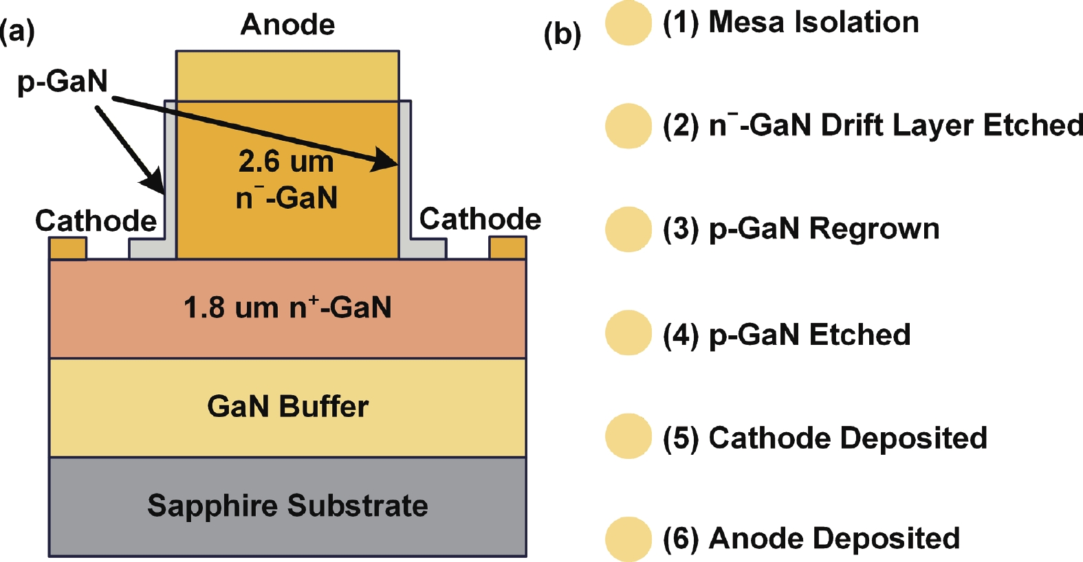
Fig. 1.
(Color online) (a) Cross-sectional schematic diagram of quasi-vertical SBDs with p-GaN sidewall. (b) Main fabrication steps for quasi-vertical SBDs with p-GaN sidewall.
ARTICLES
Yinhe Wu1, Haoyin Ke1, Yu Fang2, Chenjun Xu1, Xiufeng Song2, Teng Jiang1, Weihang Zhang1, Shenglei Zhao2, , Yue Hao2 and Jincheng Zhang2
Corresponding author: S. Zhao, Email: slzhao@xidian.edu.cn
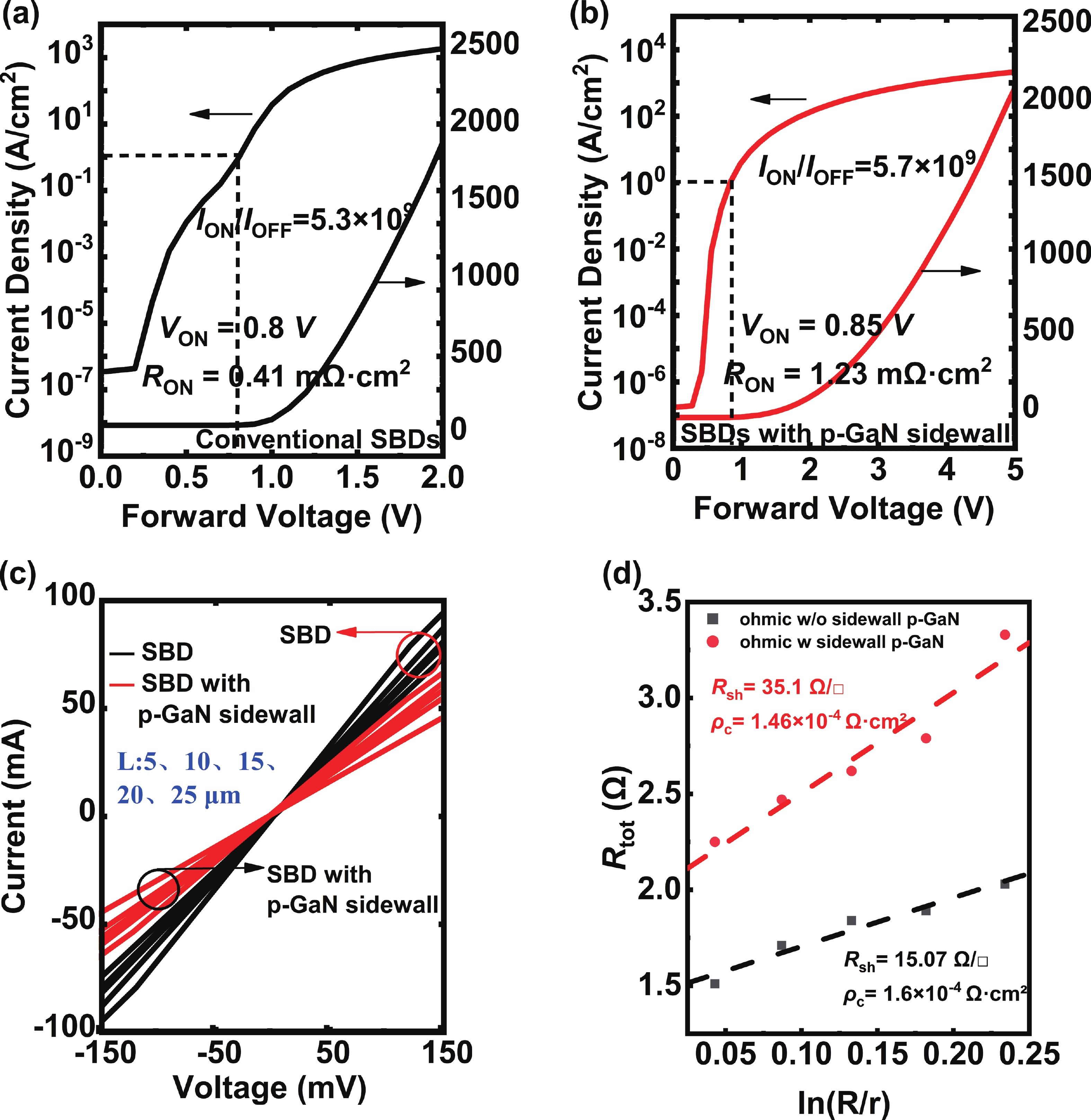
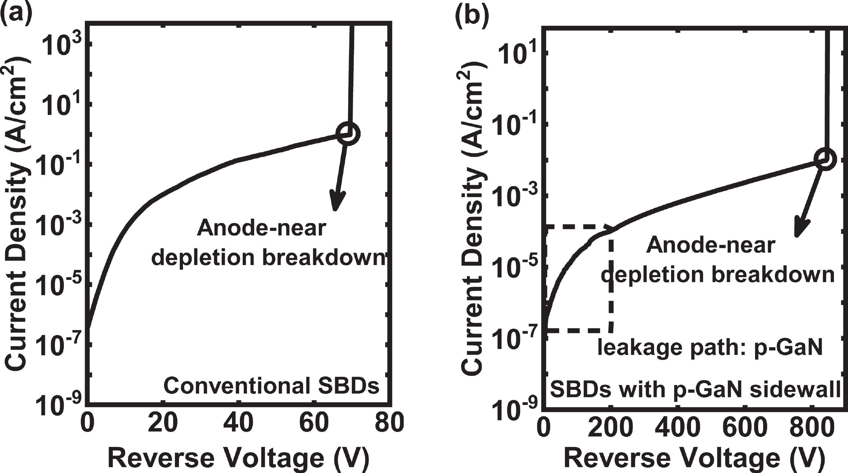
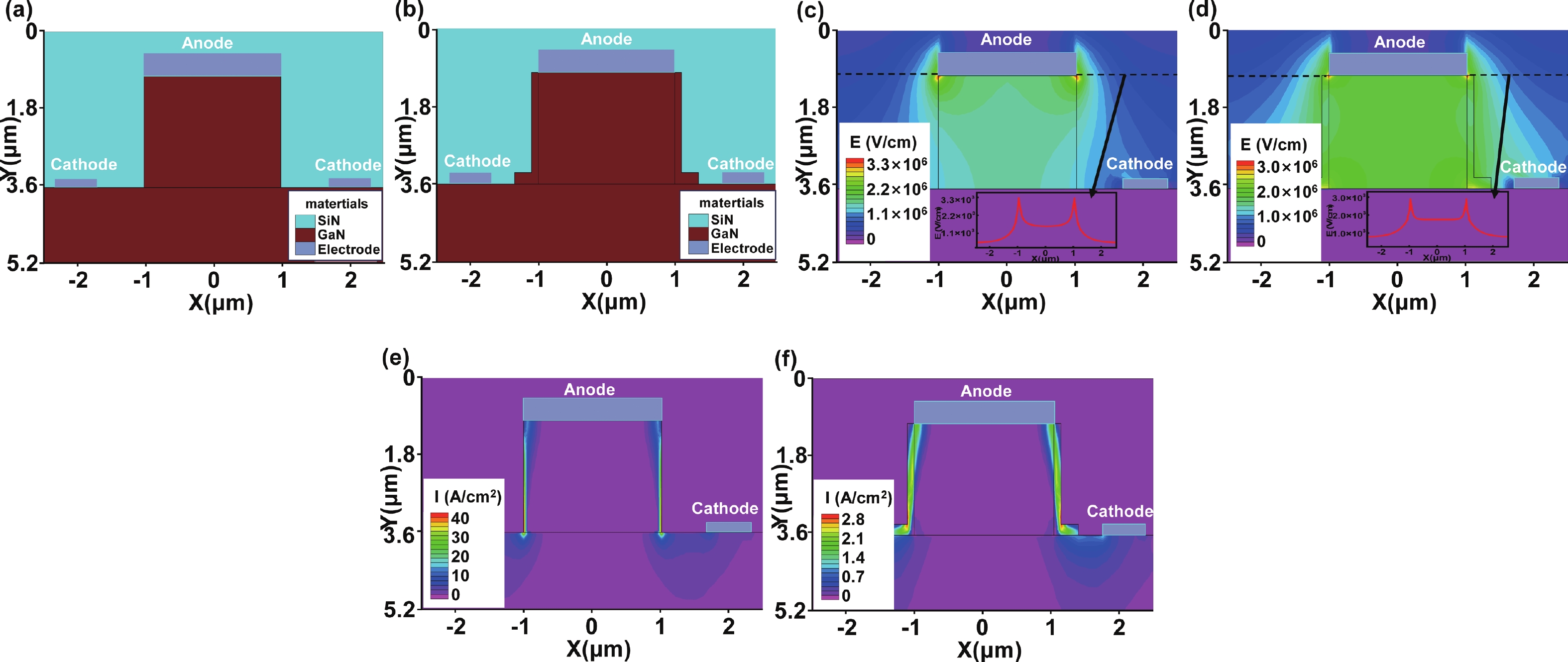
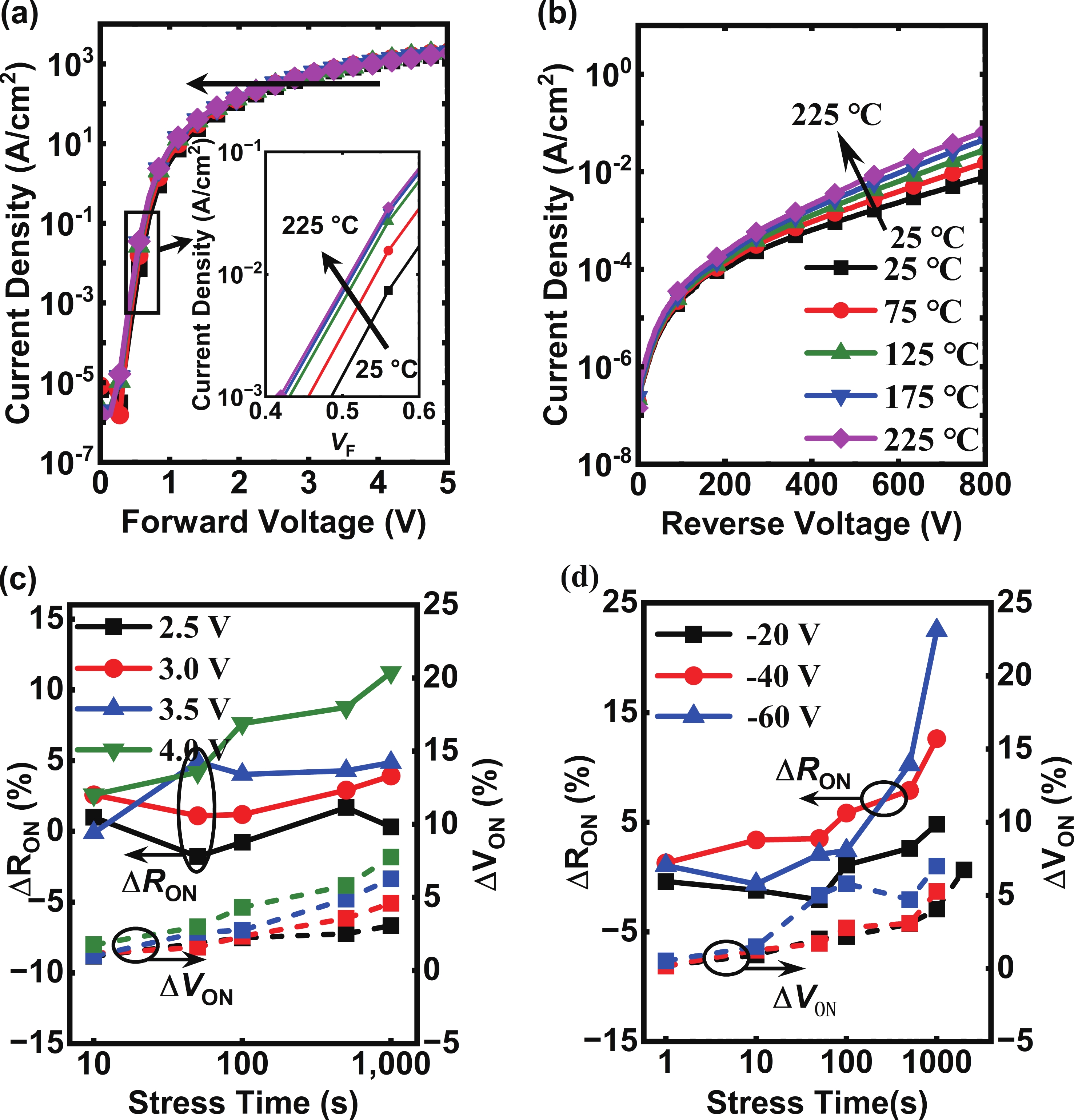
Abstract: This work demonstrates high-performance quasi-vertical GaN Schottky barrier diodes (SBDs) on sapphire substrates utilizing a regrown p-GaN sidewall structure. The regrown p-GaN sidewall alleviates electric-field crowding at the Schottky-contact edge and suppresses sidewall-associated reverse leakage, leading to a dramatic enhancement in breakdown voltage (BV) from 71 to 847 V. Furthermore, the reverse leakage current density is suppressed by five orders of magnitude, decreasing from 0.29 to 5.2 × 10⁻⁶ A/cm2 at a cathode bias of −50 V. Two-dimensional TCAD simulations were performed to verify the field-modulation effect of the p-GaN sidewall. The quasi-vertical SBDs with p-GaN sidewall demonstrate robust stability under both thermal and reverse-bias stress, highlighting the potential of regrown sidewall architectures for the next generation of GaN-on-sapphire power electronics.
Keywords: GaN, Quasi-vertical SBDs, p-GaN sidewall, breakdown voltage
| [1] |
Chen K J, Häberlen O, Lidow A, et al. GaN-on-Si power technology: Devices and applications. IEEE Trans Electron Devices, 2017, 64(3): 779 doi: 10.1109/TED.2017.2657579
|
| [2] |
Zhang Y H, Udrea F, Wang H. Multidimensional device architectures for efficient power electronics. Nat Electron, 2022, 5(11): 723 doi: 10.1038/s41928-022-00860-5
|
| [3] |
Uesugi T, Kachi T. Which are the future GaN power devices for automotive applications, lateral structures or vertical structures? CS MANTECH Conference, 2011: 307
|
| [4] |
Fu H Q, Fu K, Chowdhury S, et al. Vertical GaN power devices: Device principles and fabrication technologies: Part II. IEEE Trans Electron Devices, 2021, 68(7): 3212 doi: 10.1109/TED.2021.3083209
|
| [5] |
Zhang Y H, Sun M, Liu Z H, et al. Electrothermal simulation and thermal performance study of GaN vertical and lateral power transistors. IEEE Trans Electron Devices, 2013, 60(7): 2224 doi: 10.1109/TED.2013.2261072
|
| [6] |
Hu J, Zhang Y H, Sun M, et al. Materials and processing issues in vertical GaN power electronics. Mater Sci Semicond Process, 2018, 78: 75 doi: 10.1016/j.mssp.2017.09.033
|
| [7] |
Witte W, Fahle D, Koch H, et al. Electrical properties of quasi-vertical Schottky diodes. Semicond Sci Technol, 2012, 27(8): 085015 doi: 10.1088/0268-1242/27/8/085015
|
| [8] |
Zhang Y H, Sun M, Wong H Y, et al. Origin and control of OFF-state leakage current in GaN-on-Si vertical diodes. IEEE Trans Electron Devices, 2015, 62(7): 2155 doi: 10.1109/TED.2015.2426711
|
| [9] |
Sun Y, Kang X W, Zheng Y K, et al. Review of the recent progress on GaN-based vertical power Schottky barrier diodes (SBDs). Electronics, 2019, 8(5): 575 doi: 10.3390/electronics8050575
|
| [10] |
Xu R, Chen P, Liu M H, et al. 1.4-kV quasi-vertical GaN Schottky barrier diode with reverse p-n junction termination. IEEE J Electron Devices Soc, 2020, 8: 316 doi: 10.1109/JEDS.2020.2980759
|
| [11] |
Guo X L, Zhong Y Z, Zhou Y, et al. Nitrogen-implanted guard rings for 600-V quasi-vertical GaN-on-Si Schottky barrier diodes with a BFOM of 0.26 GW/ cm2. IEEE Trans Electron Devices, 2021, 68(11): 5682 doi: 10.1109/TED.2021.3108951
|
| [12] |
Zhou F, Xu W Z, Ren F F, et al. High-voltage quasi-vertical GaN junction barrier Schottky diode with fast switching characteristics. IEEE Electron Device Lett, 2021, 42(7): 974 doi: 10.1109/LED.2021.3078477
|
| [13] |
Huang F P, Chu C S, Wang Z Z, et al. 1.43 kV GaN-based MIS Schottky barrier diodes. J Phys D Appl Phys, 2024, 57(18): 185102 doi: 10.1088/1361-6463/ad256c
|
| [14] |
Sun Y, Kang X W, Zheng Y K, et al. Optimization of mesa etch for a quasi-vertical GaN Schottky barrier diode (SBD) by inductively coupled plasma (ICP) and device characteristics. Nanomaterials, 2020, 10(4): 657 doi: 10.3390/nano10040657
|
| [15] |
Fu K, Fu H Q, Huang X Q, et al. Reverse leakage analysis for As-grown and regrown vertical GaN-on-GaN Schottky barrier diodes. IEEE J Electron Devices Soc, 2020, 8: 74 doi: 10.1109/JEDS.2020.2963902
|
| [16] |
Wu Z, Ma Q, Fu S, et al. Quasi-vertical GaN Schottky barrier diode on sapphire substrate with 109 high ION/IOFF and excellent forward performance. 20th China International Forum on Solid State Lighting & 9th International Forum on Wide Bandgap Semiconductors (SSLCHINA: IFWS), 2023: 208
|
| [17] |
Tomiya S, Hino T, Goto S, et al. Dislocation related issues in the degradation of GaN-based laser diodes. IEEE J Sel Top Quantum Electron, 2004, 10(6): 1277 doi: 10.1109/JSTQE.2004.837735
|
| [18] |
Fu H Q, Fu K, Yang C, et al. Selective area regrowth and doping for vertical gallium nitride power devices: Materials challenges and recent progress. Mater Today, 2021, 49: 296 doi: 10.1016/j.mattod.2021.04.011
|
| [19] |
Qin Y, Xiao M, Zhang R Z, et al. 1 kV GaN-on-Si quasi-vertical Schottky rectifier. IEEE Electron Device Lett, 2023, 44(7): 1052 doi: 10.1109/LED.2023.3282025
|
| [20] |
Huang F P, Chu C S, Zhang Y H, et al. GaN-based quasi-vertical Schottky barrier diodes with the sidewall field plate termination for obtaining low leakage current and high breakdown voltage. 2021 IEEE 1st International Power Electronics and Application Symposium (PEAS), 2021: 1
|
| [21] |
Guo X L, Zhong Y Z, Chen X, et al. Reverse leakage and breakdown mechanisms of vertical GaN-on-Si Schottky barrier diodes with and without implanted termination. Appl Phys Lett, 2021, 118(24): 243501 doi: 10.1063/5.0049706
|
| [22] |
Chen J B, Liu Z H, Wang H Y, et al. Determination of the leakage current transport mechanisms in quasi-vertical GaN–on–Si Schottky barrier diodes (SBDs) at low and high reverse biases and varied temperatures. Appl Phys Express, 2021, 14(10): 104002 doi: 10.35848/1882-0786/ac2260
|
| [23] |
Kang X W, Sun Y, Zheng Y K, et al. Low leakage and high forward current density quasi-vertical GaN Schottky barrier diode with post-mesa nitridation. IEEE Trans Electron Devices, 2021, 68(3): 1369 doi: 10.1109/TED.2021.3050739
|
| [24] |
Tallarico A N, Stoffels S, Magnone P, et al. Reliability of Au-free AlGaN/GaN-on-silicon Schottky barrier diodes under ON-state stress. IEEE Trans Electron Devices, 2016, 63(2): 723 doi: 10.1109/TED.2015.2507867
|
| [25] |
Hu J, Stoffels S, Lenci S, et al. Investigation of constant voltage off-state stress on Au-free AlGaN/GaN Schottky barrier diodes. Jpn J Appl Phys, 2015, 54(4S): 04DF07 doi: 10.7567/JJAP.54.04DF07
|
| [1] |
Chen K J, Häberlen O, Lidow A, et al. GaN-on-Si power technology: Devices and applications. IEEE Trans Electron Devices, 2017, 64(3): 779 doi: 10.1109/TED.2017.2657579
|
| [2] |
Zhang Y H, Udrea F, Wang H. Multidimensional device architectures for efficient power electronics. Nat Electron, 2022, 5(11): 723 doi: 10.1038/s41928-022-00860-5
|
| [3] |
Uesugi T, Kachi T. Which are the future GaN power devices for automotive applications, lateral structures or vertical structures? CS MANTECH Conference, 2011: 307
|
| [4] |
Fu H Q, Fu K, Chowdhury S, et al. Vertical GaN power devices: Device principles and fabrication technologies: Part II. IEEE Trans Electron Devices, 2021, 68(7): 3212 doi: 10.1109/TED.2021.3083209
|
| [5] |
Zhang Y H, Sun M, Liu Z H, et al. Electrothermal simulation and thermal performance study of GaN vertical and lateral power transistors. IEEE Trans Electron Devices, 2013, 60(7): 2224 doi: 10.1109/TED.2013.2261072
|
| [6] |
Hu J, Zhang Y H, Sun M, et al. Materials and processing issues in vertical GaN power electronics. Mater Sci Semicond Process, 2018, 78: 75 doi: 10.1016/j.mssp.2017.09.033
|
| [7] |
Witte W, Fahle D, Koch H, et al. Electrical properties of quasi-vertical Schottky diodes. Semicond Sci Technol, 2012, 27(8): 085015 doi: 10.1088/0268-1242/27/8/085015
|
| [8] |
Zhang Y H, Sun M, Wong H Y, et al. Origin and control of OFF-state leakage current in GaN-on-Si vertical diodes. IEEE Trans Electron Devices, 2015, 62(7): 2155 doi: 10.1109/TED.2015.2426711
|
| [9] |
Sun Y, Kang X W, Zheng Y K, et al. Review of the recent progress on GaN-based vertical power Schottky barrier diodes (SBDs). Electronics, 2019, 8(5): 575 doi: 10.3390/electronics8050575
|
| [10] |
Xu R, Chen P, Liu M H, et al. 1.4-kV quasi-vertical GaN Schottky barrier diode with reverse p-n junction termination. IEEE J Electron Devices Soc, 2020, 8: 316 doi: 10.1109/JEDS.2020.2980759
|
| [11] |
Guo X L, Zhong Y Z, Zhou Y, et al. Nitrogen-implanted guard rings for 600-V quasi-vertical GaN-on-Si Schottky barrier diodes with a BFOM of 0.26 GW/ cm2. IEEE Trans Electron Devices, 2021, 68(11): 5682 doi: 10.1109/TED.2021.3108951
|
| [12] |
Zhou F, Xu W Z, Ren F F, et al. High-voltage quasi-vertical GaN junction barrier Schottky diode with fast switching characteristics. IEEE Electron Device Lett, 2021, 42(7): 974 doi: 10.1109/LED.2021.3078477
|
| [13] |
Huang F P, Chu C S, Wang Z Z, et al. 1.43 kV GaN-based MIS Schottky barrier diodes. J Phys D Appl Phys, 2024, 57(18): 185102 doi: 10.1088/1361-6463/ad256c
|
| [14] |
Sun Y, Kang X W, Zheng Y K, et al. Optimization of mesa etch for a quasi-vertical GaN Schottky barrier diode (SBD) by inductively coupled plasma (ICP) and device characteristics. Nanomaterials, 2020, 10(4): 657 doi: 10.3390/nano10040657
|
| [15] |
Fu K, Fu H Q, Huang X Q, et al. Reverse leakage analysis for As-grown and regrown vertical GaN-on-GaN Schottky barrier diodes. IEEE J Electron Devices Soc, 2020, 8: 74 doi: 10.1109/JEDS.2020.2963902
|
| [16] |
Wu Z, Ma Q, Fu S, et al. Quasi-vertical GaN Schottky barrier diode on sapphire substrate with 109 high ION/IOFF and excellent forward performance. 20th China International Forum on Solid State Lighting & 9th International Forum on Wide Bandgap Semiconductors (SSLCHINA: IFWS), 2023: 208
|
| [17] |
Tomiya S, Hino T, Goto S, et al. Dislocation related issues in the degradation of GaN-based laser diodes. IEEE J Sel Top Quantum Electron, 2004, 10(6): 1277 doi: 10.1109/JSTQE.2004.837735
|
| [18] |
Fu H Q, Fu K, Yang C, et al. Selective area regrowth and doping for vertical gallium nitride power devices: Materials challenges and recent progress. Mater Today, 2021, 49: 296 doi: 10.1016/j.mattod.2021.04.011
|
| [19] |
Qin Y, Xiao M, Zhang R Z, et al. 1 kV GaN-on-Si quasi-vertical Schottky rectifier. IEEE Electron Device Lett, 2023, 44(7): 1052 doi: 10.1109/LED.2023.3282025
|
| [20] |
Huang F P, Chu C S, Zhang Y H, et al. GaN-based quasi-vertical Schottky barrier diodes with the sidewall field plate termination for obtaining low leakage current and high breakdown voltage. 2021 IEEE 1st International Power Electronics and Application Symposium (PEAS), 2021: 1
|
| [21] |
Guo X L, Zhong Y Z, Chen X, et al. Reverse leakage and breakdown mechanisms of vertical GaN-on-Si Schottky barrier diodes with and without implanted termination. Appl Phys Lett, 2021, 118(24): 243501 doi: 10.1063/5.0049706
|
| [22] |
Chen J B, Liu Z H, Wang H Y, et al. Determination of the leakage current transport mechanisms in quasi-vertical GaN–on–Si Schottky barrier diodes (SBDs) at low and high reverse biases and varied temperatures. Appl Phys Express, 2021, 14(10): 104002 doi: 10.35848/1882-0786/ac2260
|
| [23] |
Kang X W, Sun Y, Zheng Y K, et al. Low leakage and high forward current density quasi-vertical GaN Schottky barrier diode with post-mesa nitridation. IEEE Trans Electron Devices, 2021, 68(3): 1369 doi: 10.1109/TED.2021.3050739
|
| [24] |
Tallarico A N, Stoffels S, Magnone P, et al. Reliability of Au-free AlGaN/GaN-on-silicon Schottky barrier diodes under ON-state stress. IEEE Trans Electron Devices, 2016, 63(2): 723 doi: 10.1109/TED.2015.2507867
|
| [25] |
Hu J, Stoffels S, Lenci S, et al. Investigation of constant voltage off-state stress on Au-free AlGaN/GaN Schottky barrier diodes. Jpn J Appl Phys, 2015, 54(4S): 04DF07 doi: 10.7567/JJAP.54.04DF07
|





Article views: 13 Times PDF downloads: 7 Times Cited by: 0 Times
Received: 11 May 2026 Revised: 25 June 2026 Online: Accepted Manuscript: 24 July 2026
| Citation: |
Yinhe Wu, Haoyin Ke, Yu Fang, Chenjun Xu, Xiufeng Song, Teng Jiang, Weihang Zhang, Shenglei Zhao, Yue Hao, Jincheng Zhang. High-performance quasi-vertical GaN Schottky barrier diodes with regrown p-GaN sidewall[J]. Journal of Semiconductors, 2026, In Press. doi: 10.1088/1674-4926/26050015
****
Y H Wu, H Y Ke, Y Fang, C J Xu, X F Song, T Jiang, W H Zhang, S L Zhao, Y Hao, and J C Zhang, High-performance quasi-vertical GaN Schottky barrier diodes with regrown p-GaN sidewall[J]. J. Semicond., 2026, accepted doi: 10.1088/1674-4926/26050015

|
 Yinhe Wu was born in Yuncheng, Shanxi, China, in 1991. He received the Ph.D. degree in engineering from Xidian University, Xi’an, China, in 2022. He is currently an Associate Professor with the Guangzhou Institute of Technology, Xidian University, Guangzhou, China. His research interests mainly focus on wide bandgap (WBG) semiconductor power devices and integrated circuit design
 Shenglei Zhao received the Ph.D. degree from Xidian University, Xi'an, China, in 2015. He is currently a Professor at the School of Microelectronics, Xidian University. His research interests include lateral GaN HEMTs, vertical GaN power devices, and GaN device reliability
| [1] |
Chen K J, Häberlen O, Lidow A, et al. GaN-on-Si power technology: Devices and applications. IEEE Trans Electron Devices, 2017, 64(3): 779 doi: 10.1109/TED.2017.2657579
|
| [2] |
Zhang Y H, Udrea F, Wang H. Multidimensional device architectures for efficient power electronics. Nat Electron, 2022, 5(11): 723 doi: 10.1038/s41928-022-00860-5
|
| [3] |
Uesugi T, Kachi T. Which are the future GaN power devices for automotive applications, lateral structures or vertical structures? CS MANTECH Conference, 2011: 307
|
| [4] |
Fu H Q, Fu K, Chowdhury S, et al. Vertical GaN power devices: Device principles and fabrication technologies: Part II. IEEE Trans Electron Devices, 2021, 68(7): 3212 doi: 10.1109/TED.2021.3083209
|
| [5] |
Zhang Y H, Sun M, Liu Z H, et al. Electrothermal simulation and thermal performance study of GaN vertical and lateral power transistors. IEEE Trans Electron Devices, 2013, 60(7): 2224 doi: 10.1109/TED.2013.2261072
|
| [6] |
Hu J, Zhang Y H, Sun M, et al. Materials and processing issues in vertical GaN power electronics. Mater Sci Semicond Process, 2018, 78: 75 doi: 10.1016/j.mssp.2017.09.033
|
| [7] |
Witte W, Fahle D, Koch H, et al. Electrical properties of quasi-vertical Schottky diodes. Semicond Sci Technol, 2012, 27(8): 085015 doi: 10.1088/0268-1242/27/8/085015
|
| [8] |
Zhang Y H, Sun M, Wong H Y, et al. Origin and control of OFF-state leakage current in GaN-on-Si vertical diodes. IEEE Trans Electron Devices, 2015, 62(7): 2155 doi: 10.1109/TED.2015.2426711
|
| [9] |
Sun Y, Kang X W, Zheng Y K, et al. Review of the recent progress on GaN-based vertical power Schottky barrier diodes (SBDs). Electronics, 2019, 8(5): 575 doi: 10.3390/electronics8050575
|
| [10] |
Xu R, Chen P, Liu M H, et al. 1.4-kV quasi-vertical GaN Schottky barrier diode with reverse p-n junction termination. IEEE J Electron Devices Soc, 2020, 8: 316 doi: 10.1109/JEDS.2020.2980759
|
| [11] |
Guo X L, Zhong Y Z, Zhou Y, et al. Nitrogen-implanted guard rings for 600-V quasi-vertical GaN-on-Si Schottky barrier diodes with a BFOM of 0.26 GW/ cm2. IEEE Trans Electron Devices, 2021, 68(11): 5682 doi: 10.1109/TED.2021.3108951
|
| [12] |
Zhou F, Xu W Z, Ren F F, et al. High-voltage quasi-vertical GaN junction barrier Schottky diode with fast switching characteristics. IEEE Electron Device Lett, 2021, 42(7): 974 doi: 10.1109/LED.2021.3078477
|
| [13] |
Huang F P, Chu C S, Wang Z Z, et al. 1.43 kV GaN-based MIS Schottky barrier diodes. J Phys D Appl Phys, 2024, 57(18): 185102 doi: 10.1088/1361-6463/ad256c
|
| [14] |
Sun Y, Kang X W, Zheng Y K, et al. Optimization of mesa etch for a quasi-vertical GaN Schottky barrier diode (SBD) by inductively coupled plasma (ICP) and device characteristics. Nanomaterials, 2020, 10(4): 657 doi: 10.3390/nano10040657
|
| [15] |
Fu K, Fu H Q, Huang X Q, et al. Reverse leakage analysis for As-grown and regrown vertical GaN-on-GaN Schottky barrier diodes. IEEE J Electron Devices Soc, 2020, 8: 74 doi: 10.1109/JEDS.2020.2963902
|
| [16] |
Wu Z, Ma Q, Fu S, et al. Quasi-vertical GaN Schottky barrier diode on sapphire substrate with 109 high ION/IOFF and excellent forward performance. 20th China International Forum on Solid State Lighting & 9th International Forum on Wide Bandgap Semiconductors (SSLCHINA: IFWS), 2023: 208
|
| [17] |
Tomiya S, Hino T, Goto S, et al. Dislocation related issues in the degradation of GaN-based laser diodes. IEEE J Sel Top Quantum Electron, 2004, 10(6): 1277 doi: 10.1109/JSTQE.2004.837735
|
| [18] |
Fu H Q, Fu K, Yang C, et al. Selective area regrowth and doping for vertical gallium nitride power devices: Materials challenges and recent progress. Mater Today, 2021, 49: 296 doi: 10.1016/j.mattod.2021.04.011
|
| [19] |
Qin Y, Xiao M, Zhang R Z, et al. 1 kV GaN-on-Si quasi-vertical Schottky rectifier. IEEE Electron Device Lett, 2023, 44(7): 1052 doi: 10.1109/LED.2023.3282025
|
| [20] |
Huang F P, Chu C S, Zhang Y H, et al. GaN-based quasi-vertical Schottky barrier diodes with the sidewall field plate termination for obtaining low leakage current and high breakdown voltage. 2021 IEEE 1st International Power Electronics and Application Symposium (PEAS), 2021: 1
|
| [21] |
Guo X L, Zhong Y Z, Chen X, et al. Reverse leakage and breakdown mechanisms of vertical GaN-on-Si Schottky barrier diodes with and without implanted termination. Appl Phys Lett, 2021, 118(24): 243501 doi: 10.1063/5.0049706
|
| [22] |
Chen J B, Liu Z H, Wang H Y, et al. Determination of the leakage current transport mechanisms in quasi-vertical GaN–on–Si Schottky barrier diodes (SBDs) at low and high reverse biases and varied temperatures. Appl Phys Express, 2021, 14(10): 104002 doi: 10.35848/1882-0786/ac2260
|
| [23] |
Kang X W, Sun Y, Zheng Y K, et al. Low leakage and high forward current density quasi-vertical GaN Schottky barrier diode with post-mesa nitridation. IEEE Trans Electron Devices, 2021, 68(3): 1369 doi: 10.1109/TED.2021.3050739
|
| [24] |
Tallarico A N, Stoffels S, Magnone P, et al. Reliability of Au-free AlGaN/GaN-on-silicon Schottky barrier diodes under ON-state stress. IEEE Trans Electron Devices, 2016, 63(2): 723 doi: 10.1109/TED.2015.2507867
|
| [25] |
Hu J, Stoffels S, Lenci S, et al. Investigation of constant voltage off-state stress on Au-free AlGaN/GaN Schottky barrier diodes. Jpn J Appl Phys, 2015, 54(4S): 04DF07 doi: 10.7567/JJAP.54.04DF07
|

 WeChat ID
Journal of Semiconductors © 2017 All Rights Reserved 京ICP备05085259号-2

 DownLoad:

