


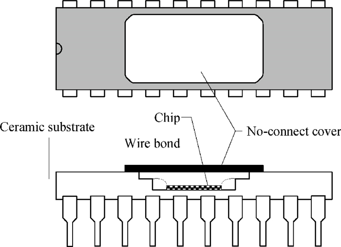
Fig. 1.
A device using a CDIP with 20 pins and a no-connect metal cover.
SEMICONDUCTOR DEVICES
Song Li, Chuanbin Zeng, Jiajun Luo and Zhengsheng Han
Corresponding author: Li Song, Email:lisong@ime.ac.cn
Abstract: The human body model (HBM) stress of a no-connect metal cover is tested to obtain the characteristics of abnormal electrostatic discharge, including current waveforms and peak current under varied stress voltage and device failure voltage. A new discharge model called the "sparkover-induced model" is proposed based on the results. Then, failure mechanism analysis and model simulation are performed to prove that the transient peak current caused by a sparkover of low arc impedance will result in the devices' premature damage when the potential difference between the no-connect metal cover and the chip exceeds the threshold voltage of sparkover.
Key words: electrostatic discharge, human body model, no-connect metal cover, sparkover
| [1] |
Fang R, Wang J, Huang L, et al. The development of electronic packaging. Science & Technology Association Forum, 2012, (2):84
|
| [2] |
Inspection criteria for microelectronic packages and covers. JEDEC Solid State Technology Association, May 2011
|
| [3] |
MIL-STD-883H. Departments and Agencies of the Department of Defense, February 2010
|
| [4] |
ESDA/JEDEC joint standard for electrostatic discharge sensitivity testing-human body model (HBM)-component level. ESD Association & JEDEC Solid State Technology Association, November 2011
|
| [5] |
Wen Y L, Ming D K. Abnormal ESD failure mechanism in high-pin-count BGA packaged ICs due to stressing nonconnected balls. IEEE Trans Device Mater Reliab, 2004, 4(1):24 doi: 10.1109/TDMR.2004.824362
|
| [6] |
Kunz H, Duvvury C, Brodsky J, et al. HBM stress of no-connect IC pins and subsequent arc-over events that lead to human-metal-discharge-like events into unstressed neighbor pins. Electrical Overstress/Electrostatic Discharge Symposium, 2006 https://www.infona.pl/resource/bwmeta1.element.ieee-art-000005256807
|
| [7] |
Kaschani K T, Schimon M, Hofmann M, et al. ESD damage due to HBM stressing of non-connected pins. Electrical Overstress/Electrostatic Discharge Symposium, 2006 http://ieeexplore.ieee.org/document/5256806/keywords
|
| [8] |
ESD association technical report for the protection of electrostatic discharge susceptible items-human metal model (HMM). Electrostatic Discharge Association, 2009
|
| [9] |
IEC 61000-4-2: electromagnetic compatibility(emc)-part 4-2: testing and measurement techniques-electrostatic discharge immunity test. IEC International Standard, 2008
|
| [10] |
Field-induced charged-device model test method for electrostatic-discharge-withstand thresholds of microelectronic components. JEDEC Solid State Technology Association, December 2009
|
| [11] |
ESD association standard for electrostatic discharge sensitivity testing-charged device model (CDM)-component level. Electrostatic Discharge Association, July 2009
|
| [12] |
Muhonen K, Peachey N, Testin A. Human metal model (HMM) testing, challenges to using ESD guns. Electrical Overstress/Electrostatic Discharge Symposium, 2009 https://www.infona.pl/resource/bwmeta1.element.ieee-art-000005340100
|
| [13] |
Karp J, Kireev V, Tsaggaris D, et al. Effect of flip-chip package parameters on CDM discharge. Electrical Overstress/Electrostatic Discharge Symposium, 2008 http://ieeexplore.ieee.org/document/4772108/authors
|
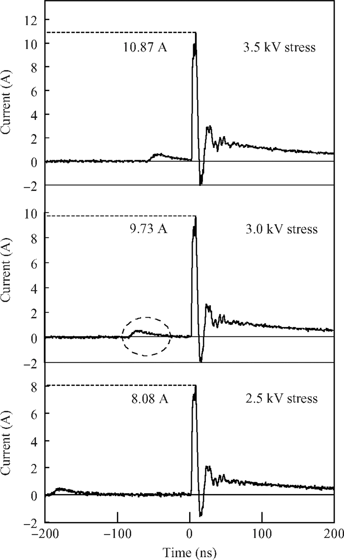
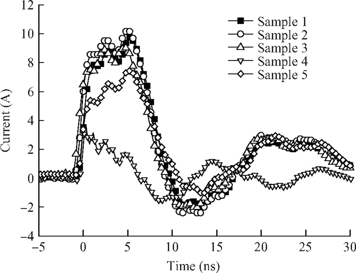
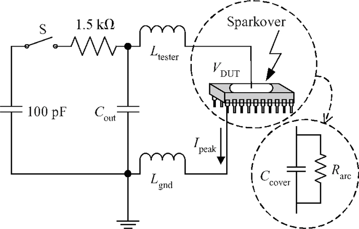
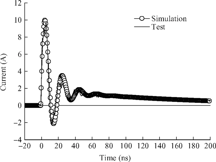

Table 1. Partial test results.

|
Table 2. Test results and chip area of all tested samples.

|
| [1] |
Fang R, Wang J, Huang L, et al. The development of electronic packaging. Science & Technology Association Forum, 2012, (2):84
|
| [2] |
Inspection criteria for microelectronic packages and covers. JEDEC Solid State Technology Association, May 2011
|
| [3] |
MIL-STD-883H. Departments and Agencies of the Department of Defense, February 2010
|
| [4] |
ESDA/JEDEC joint standard for electrostatic discharge sensitivity testing-human body model (HBM)-component level. ESD Association & JEDEC Solid State Technology Association, November 2011
|
| [5] |
Wen Y L, Ming D K. Abnormal ESD failure mechanism in high-pin-count BGA packaged ICs due to stressing nonconnected balls. IEEE Trans Device Mater Reliab, 2004, 4(1):24 doi: 10.1109/TDMR.2004.824362
|
| [6] |
Kunz H, Duvvury C, Brodsky J, et al. HBM stress of no-connect IC pins and subsequent arc-over events that lead to human-metal-discharge-like events into unstressed neighbor pins. Electrical Overstress/Electrostatic Discharge Symposium, 2006 https://www.infona.pl/resource/bwmeta1.element.ieee-art-000005256807
|
| [7] |
Kaschani K T, Schimon M, Hofmann M, et al. ESD damage due to HBM stressing of non-connected pins. Electrical Overstress/Electrostatic Discharge Symposium, 2006 http://ieeexplore.ieee.org/document/5256806/keywords
|
| [8] |
ESD association technical report for the protection of electrostatic discharge susceptible items-human metal model (HMM). Electrostatic Discharge Association, 2009
|
| [9] |
IEC 61000-4-2: electromagnetic compatibility(emc)-part 4-2: testing and measurement techniques-electrostatic discharge immunity test. IEC International Standard, 2008
|
| [10] |
Field-induced charged-device model test method for electrostatic-discharge-withstand thresholds of microelectronic components. JEDEC Solid State Technology Association, December 2009
|
| [11] |
ESD association standard for electrostatic discharge sensitivity testing-charged device model (CDM)-component level. Electrostatic Discharge Association, July 2009
|
| [12] |
Muhonen K, Peachey N, Testin A. Human metal model (HMM) testing, challenges to using ESD guns. Electrical Overstress/Electrostatic Discharge Symposium, 2009 https://www.infona.pl/resource/bwmeta1.element.ieee-art-000005340100
|
| [13] |
Karp J, Kireev V, Tsaggaris D, et al. Effect of flip-chip package parameters on CDM discharge. Electrical Overstress/Electrostatic Discharge Symposium, 2008 http://ieeexplore.ieee.org/document/4772108/authors
|


Article views: 3333 Times PDF downloads: 19 Times Cited by: 0 Times
Received: 07 January 2013 Revised: 22 March 2013 Online: Published: 01 August 2013
| Citation: |
Song Li, Chuanbin Zeng, Jiajun Luo, Zhengsheng Han. The abnormal electrostatic discharge of a no-connect metal cover in a ceramic packaging device[J]. Journal of Semiconductors, 2013, 34(8): 084007. doi: 10.1088/1674-4926/34/8/084007
****
S Li, C B Zeng, J J Luo, Z S Han. The abnormal electrostatic discharge of a no-connect metal cover in a ceramic packaging device[J]. J. Semicond., 2013, 34(8): 084007. doi: 10.1088/1674-4926/34/8/084007.

|
| [1] |
Fang R, Wang J, Huang L, et al. The development of electronic packaging. Science & Technology Association Forum, 2012, (2):84
|
| [2] |
Inspection criteria for microelectronic packages and covers. JEDEC Solid State Technology Association, May 2011
|
| [3] |
MIL-STD-883H. Departments and Agencies of the Department of Defense, February 2010
|
| [4] |
ESDA/JEDEC joint standard for electrostatic discharge sensitivity testing-human body model (HBM)-component level. ESD Association & JEDEC Solid State Technology Association, November 2011
|
| [5] |
Wen Y L, Ming D K. Abnormal ESD failure mechanism in high-pin-count BGA packaged ICs due to stressing nonconnected balls. IEEE Trans Device Mater Reliab, 2004, 4(1):24 doi: 10.1109/TDMR.2004.824362
|
| [6] |
Kunz H, Duvvury C, Brodsky J, et al. HBM stress of no-connect IC pins and subsequent arc-over events that lead to human-metal-discharge-like events into unstressed neighbor pins. Electrical Overstress/Electrostatic Discharge Symposium, 2006 https://www.infona.pl/resource/bwmeta1.element.ieee-art-000005256807
|
| [7] |
Kaschani K T, Schimon M, Hofmann M, et al. ESD damage due to HBM stressing of non-connected pins. Electrical Overstress/Electrostatic Discharge Symposium, 2006 http://ieeexplore.ieee.org/document/5256806/keywords
|
| [8] |
ESD association technical report for the protection of electrostatic discharge susceptible items-human metal model (HMM). Electrostatic Discharge Association, 2009
|
| [9] |
IEC 61000-4-2: electromagnetic compatibility(emc)-part 4-2: testing and measurement techniques-electrostatic discharge immunity test. IEC International Standard, 2008
|
| [10] |
Field-induced charged-device model test method for electrostatic-discharge-withstand thresholds of microelectronic components. JEDEC Solid State Technology Association, December 2009
|
| [11] |
ESD association standard for electrostatic discharge sensitivity testing-charged device model (CDM)-component level. Electrostatic Discharge Association, July 2009
|
| [12] |
Muhonen K, Peachey N, Testin A. Human metal model (HMM) testing, challenges to using ESD guns. Electrical Overstress/Electrostatic Discharge Symposium, 2009 https://www.infona.pl/resource/bwmeta1.element.ieee-art-000005340100
|
| [13] |
Karp J, Kireev V, Tsaggaris D, et al. Effect of flip-chip package parameters on CDM discharge. Electrical Overstress/Electrostatic Discharge Symposium, 2008 http://ieeexplore.ieee.org/document/4772108/authors
|

 WeChat ID
Journal of Semiconductors © 2017 All Rights Reserved 京ICP备05085259号-2

 DownLoad:


