


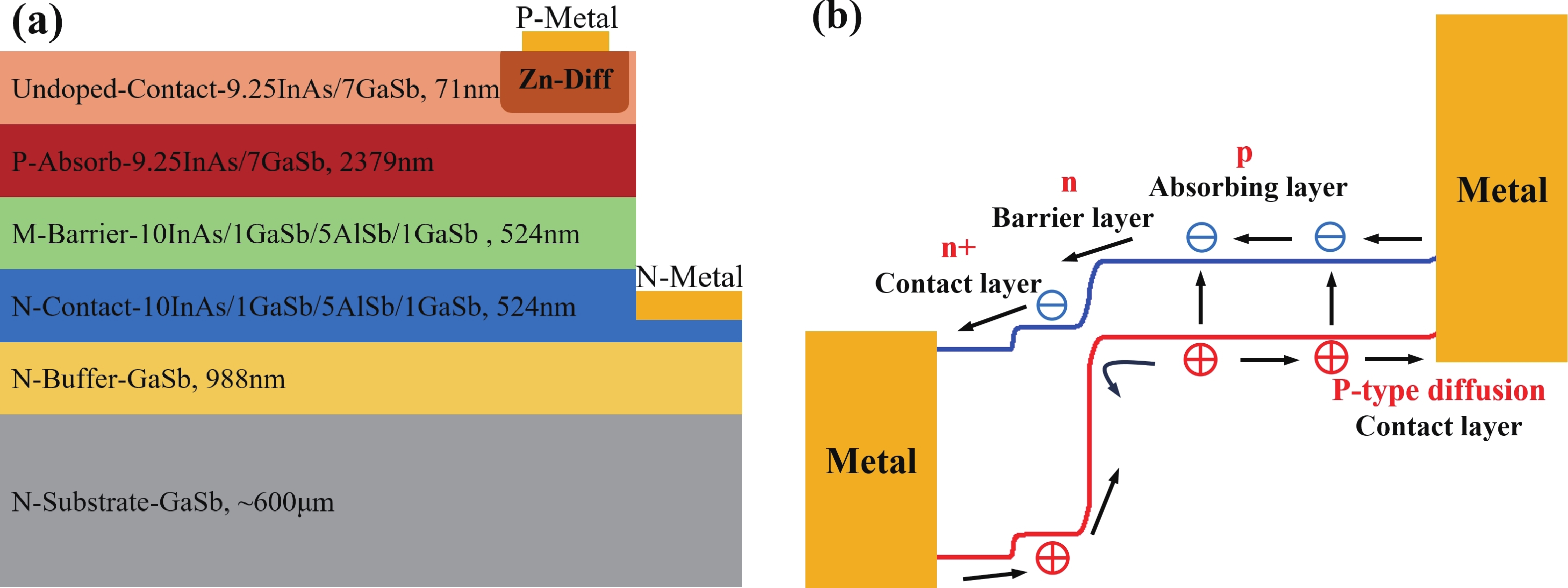
In this paper, a planar junction mid-wavelength infrared (MWIR) photodetector based on an InAs/GaSb type-Ⅱ superlattices (T2SLs) is reported. The Intrinsic-πMN superlattices was grown by the molecular beam epitaxy (MBE), followed with a ZnS layer grown by the chemical vapor deposition (CVD). The p-type contact layer was constructed by thermal diffusion in the undoped superlattices. The Zinc atom was successfully realised in to the superlattice and a PπMN T2SL structure was constructed. Furthermore, the effects of different diffusion temperatures on the dark current performance of the devices were researched. The 50% cut-off wavelength of the photodetector is 5.26 μm at 77 K with 0 V bias. The minimum dark current density is 8.67 × 10⁻⁵ A/cm2 and the maximum quantum efficiency of 42.5%, and the maximum detectivity reaches 3.90 × 1010 cm·Hz1/2/W at 77 K. The 640 × 512 focal plane arrays (FPA) based on the planner junction were fabricated afterwards. The FPA achieves a noise equivalent temperature difference (NETD) of 539 mK.
- • Uncorrected proofs: articles that have been copy edited and formatted, but have not been finalized yet. They still need to be proof-read and corrected by the author(s) and the text could still change before final publication.
- • Corrected proofs: articles that contain the authors' corrections. Final citation details, e.g. volume and/or issue number, publication year and page numbers, still need to be added and the text might change before final publication.
There are two types in Press articles:


As organic thin film transistors (OTFTs) are set to play a crucial role in flexible and cost-effective electronic applications, this paper investigates a high-mobility 6,13-bis(triisopropylsilylethynyl) Pentacene (TIPS-Pentacene) OTFT for use in flexible electronics. The development of such high-mobility devices necessitates precise device modeling to support technology optimisation and circuit design. The details of numerical simulation technique is discussed, in which, the electrical behavior of the device is well captured by fine tuning basic semiconductor equations. This technology computer-aided design (TCAD) has been validated with eprimental data. In addition, we have discussed about compact model fitting of the devices as well as parameter extraction procedure employed. This includes verification of ATLAS FEM based results against experimental data gained from fabricated OTFT devices. Simulations for p-type TFT-based inverter are also performed to assess the performance of compact model in simple circuit simulation.


Avalanche photodiode (APD) is a kind of photodetector with important applications in optical communication, LIDAR and other fields. APDs fabricated using the recently developed AlGaAsSb as the multiplication material exhibit excellent noise performance. In this work, we report a low-noise separate absorption, grading, charge, and multiplication (SAGCM) InGaAs/AlGaAsSb APD operating at 1550 nm. A double-mesa structure was fabricated to reduce the dark current. Numerical simulations were conducted to compare two different mesa-structured APDs. By analyzing the electric field distribution, it was found that the electric field at the edge of the multiplication region in the double-mesa APD is nearly 100 kV/cm lower than that of the single-mesa structure. Experimental results demonstrate that after device punch-through, the double-mesa APD’s dark current can be reduced by up to four times compared to the single-mesa APD. Quantitative analysis of the dark current components in the AlGaAsSb APD further confirms that the low sidewall electric field in the double-mesa structure effectively suppresses the trap-assisted tunneling. Additionally, noise measurements indicate a k-value of approximately 0.014, which is significantly lower than that of traditional multiplication materials. This work provides preliminary validation for further performance improvements in low noise and low dark current AlGaAsSb APDs.


Infrared and terahertz waves constitute pivotal bands within the electromagnetic spectrum, distinguished by their robust penetration capabilities and non-ionizing nature. These wavebands offer the potential for achieving high-resolution and non-destructive detection methodologies, thereby possessing considerable research significance across diverse domains including communication technologies, biomedical applications, and security screening systems. Two-dimensional materials, owing to their distinctive optoelectronic attributes, have found widespread application in photodetection endeavors. Nonetheless, their efficacy diminishes when tasked with detecting lower photon energies. Furthermore, as the landscape of device integration evolves, two-dimensional materials struggle to align with the stringent demands for device superior performance. Topological materials, with their topologically protected electronic states and non-trivial topological invariants, exhibit quantum anomalous Hall effects and ultra-high carrier mobility, providing a new approach for seeking photosensitive materials for infrared and terahertz photodetectors. This article introduces various types of topological materials and their properties, followed by an explanation of the detection mechanism and performance parameters of photodetectors. Finally, it summarizes the current research status of near-infrared to far-infrared photodetectors and terahertz photodetectors based on topological materials, discussing the challenges faced and future prospects in their development.


In this study, we present the fabrication of vertical SnO/β-Ga2O3 heterojunction diode (HJD) via radio frequency (RF) reactive magnetron sputtering. The valence and conduction band offsets between β-Ga2O3 and SnO are determined to be 2.65 and 0.75 eV, respectively, through X-ray photoelectron spectroscopy, showing a type-Ⅱ band alignment. Compared to its Schottky barrier diode (SBD) counterpart, the HJD presents a comparable specific ON-resistances (Ron,sp) of 2.8 mΩ·cm² and lower reverse leakage current (IR), leading to an enhanced reverse blocking characteristics with breakdown voltage (BV) of 1675 V and power figure of merit (PFOM) of 1.0 GW/cm². This demonstrates the high quality of the SnO/β-Ga2O3 heterojunction interface. Silvaco TCAD simulation further reveals that electric field crowding at the edge of anode for the SBD was greatly depressed by the introduction of SnO film, revealing the potential application of SnO/β-Ga2O3 heterojunction in the future β-Ga2O3-based power devices.


Currently, the global 5G network, cloud computing, and data center industries are experiencing rapid development. The continuous growth of data center traffic has driven the vigorous progress in high-speed optical transceivers for optical interconnection within data centers. The electro-absorption modulated laser (EML), which is widely used in optical fiber communications, data centers, and high-speed data transmission systems, represents a high-performance photoelectric conversion device. Compared to traditional directly modulated lasers (DMLs), EMLs demonstrate lower frequency chirp and higher modulation bandwidth, enabling support for higher data rates and longer transmission distances. This article introduces the composition, working principles, manufacturing processes, and applications of EMLs. It reviews the progress on advanced indium phosphide (InP)-based EML devices from research institutions worldwide, while summarizing and comparing data transmission rates and key technical approaches across various studies.


To address the escalating demand for high-mobility transparent and conductive oxide (TCO) films in heterojunction solar cells, multiple components doped In2O3 targets were proposed. The In2O3 targets incorporating 1 wt.% CeO2, Ta2O5 and TiO2 were sintered under different sintering temperatures and times. All the targets show the cubic bixbyite phase of In2O3. The microstructure illustrates densely packed fine grains and uniform elemental distribution. Notably, increasing the sintering temperature and holding time contributes to effective pore elimination within the targets. A relative density of greater than 99.5% is obtained for the targets sintered at 1500 °C for 4 and 6 h, and the corresponding optimum resistivity decreases from 1.068 × 10−³ Ω·cm to 9.73 × 10⁻⁴ Ω·cm. These results provide the experimental basis of fabricating In2O3-based targets for depositing high mobility TCO films by magnetron sputtering.


The radiation-sensitive field effect transistors (RADFET) radiation dosimeter is a type of radiation detector based on the total dose effects of the p-channel metal-oxide-semiconductor (PMOS) transistor. The RADFET chip was fabricated in United Microelectronics Center 8-inch process with a six-layer photomask. The chip including two identical PMOS transistors, occupies a size of 610 µm × 610 µm. Each PMOS has a W/L ratio of 300 µm/50 µm, and a 400 nm thick gate oxide, which is formed by a dry-wet-dry oxygen process. The wet oxygen-formed gate oxide with more traps can capture more holes during irradiation, thus significantly changing the PMOS threshold voltage. Pre-irradiation measurement results from ten test chips show that the initial average voltage of the PMOS is 1.961 V with a dispersion of 5.7%. The irradiation experiment is conducted in a cobalt source facility with a dose rate of 50 rad(Si)/s. During irradiation, a constant current source circuit of 10 µA was connected to monitoring the shift in threshold voltage under different total dose. When the total dose is 100 krad(Si), the shift in threshold voltage was approximately 1.37 V, which demonstrates that an excellent radiation function was achieved.


This study investigates the effect of apple extract on CoFe2O4 nanoparticles synthesized via a green self-ignition method. High resolution transmission electron microscope (HRTEM) showed nanometric particles with varied shapes, while X-ray diffraction (XRD) and Rietveld refinement confirmed a facecentered cubic (Fd3̅m) structure. Mössbauer spectroscopy revealed a Zeeman sextet pattern with only Fe3+ ions. Ultra violet vissible nearinfrared (UV–Vis–NIR) spectra indicated strong absorbance in the visible and NIR regions, suggesting optoelectronic potential. The nanoparticles demonstrated high photo-Fenton catalytic efficiency, degrading 96.88% of Methylene Blue under visible light. They also exhibited 100% adsorption capacities for Cr3+ and Pb2+, making them effective for water treatment. These properties were attributed to a large surface area (347.04 m2/g), mesoporous structure, and mixed spinel phase. ANOVA and Tukey’s honestly significant difference (HSD) tests confirmed that contact time and adsorbent dosage significantly affected pollutant removal. Additionally, strong antimicrobial activity highlighted their biotechnological relevance. The inclusion of apple extract enhanced structural and functional features, expanding application prospects in spin valves, magnetic recording, refrigeration, microwave technologies (C to Ku bands), optoelectronics, and biotechnology. Future work should explore the photo-Fenton degradation mechanism and optimize synthesis for scalable production, aiming to maximize their industrial utility.


The optical soliton characteristics of GaSb-based ~2 μm wavelength integrated optical chips have broad application prospects in optoelectronic fields such as optical communications, infrared countermeasures, and gas environment monitoring. In the research of two-section integrated optical chips, more attention is paid to their passive mode-locked characteristics. The ability of its structure to generate stable soliton transmission has not yet been studied, which will limit its further application in high-performance near-mid infrared optoelectronic technology. In this paper, we design and prepare a GaSb-based ~2 μm wavelength two-section integrated semiconductor laser chip structure, and test and analyze its related properties of soliton, including power−injection current−voltage (P−I−V), temperature and mode-locked characteristics. Experimental results show that the chip can achieve stable mode-locked operation at nearly ~2 μm wavelength and present the working characteristics of near optical soliton states and multi-peak optical soliton states. By comparing and analyzing the measured optical pulse sequence curve with the numerical fitting based on the pure fourth order soliton approximation solution, it is confirmed that the two-section integrated optical chip structure can generate stable transmission of multi-peak optical soliton. This provides a research direction for developing near-mid infrared mode-locked integrated optical chips with high-performance property of optical soliton.


To optimize turn on velocity of the SiC LIMS, we proposed a new structure for the LIMS that incorporates an optimized n+ layer and a multi-light triggered electrode design for the anode. The chip size is 5.5 mm × 5.5 mm in dimension. The experiment results indicate that the saturation laser energy required to trigger the prepared SiC LIMS has been decreased from 1.8 mJ to 40 μJ, with the forward blocking voltage of the prepared SiC LIMSs capable of withstanding over 7000 V. The leakage current is about 0.3 μA at room temperature, and the output current density achieves 4.25 kA/cm2 (with di/dt larger than 20 kA/μs).


A 4H-SiC superjunction (SJ) MOSFET (SJMOS) with integrated high-K gate dielectric and split gate (HKSG-SJMOS) is proposed in this paper. The key features of HKSG-SJMOS involve the utilization of high-K (HK) dielectric as the gate dielectric, which surrounds the source-connected split gate (SG) and metal gate. The high-K gate dielectric optimizes the electric field distribution within the drift region, creating a low-resistance conductive channel. This enhancement leads to an increase in the breakdown voltage (BV) and a reduction in the specific on resistance (Ron,sp). The introduction of split gate surrounded by high-K dielectric reduces the gate−drain capacitance (Cgd) and gate−drain charge (Qgd), which improves the switching characteristics. The simulation results indicate that compared to conventional 4H-SiC SJMOS, the HKSG-SJMOS exhibits a 110.5% enhancement in figure of merit (FOM, FOM = BV2/Ron,sp), a 93.6% reduction in the high frequency figure of merit (HFFOM) of Ron,sp·Cgd, and reductions in turn-on loss (Eon) and turn-off loss (Eoff) by 38.3% and 31.6%, respectively. Furthermore, the reverse recovery characteristics of HKSG-SJMOS has also discussed, revealing superior performance compared to conventional 4H-SiC SJMOS.


Besides the common short-channel effect (SCE) of threshold voltage (Vth) roll-off during the channel length (L) downscaling of InGaZnO (IGZO) thin-film transistors (TFTs), an opposite Vth roll-up was reported in this work. Both roll-off and roll-up effects of Vth were comparatively investigated on IGZO transistors with varied gate insulator (GI), source/drain (S/D), and device architecture. For IGZO transistors with thinner GI, the SCE was attenuated due to the enhanced gate controllability over the variation of channel carrier concentration, while the Vth roll-up became more noteworthy. The latter was found to depend on the relative ratio of S/D series resistance (RSD) over channel resistance (RCH), as verified on transistors with different S/D. Thus, an ideal S/D engineering with small RSD but weak dopant diffusion is highly expected during the downscaling of L and GI in IGZO transistors.


The unique structure and exceptional properties of two-dimensional (2D) materials offer significant potential for transformative advancements in semiconductor industry. Similar to the reliance on wafer-scale single-crystal ingots for silicon-based chips, practical applications of 2D materials at the chip level needs large-scale, high-quality production of 2D single crystals. Over the past two decades, the size of 2D single-crystals has been improved to wafer or meter scale, where the nucleation control during the growth process is particularly important. Therefore, it is essential to conduct a comprehensive review of nucleation control in 2D materials to gain fundamental insights into the growth of 2D single-crystal materials. This review mainly focuses on two aspects: controlling nucleation density to enable the growth from a single nucleus, and controlling nucleation position to achieve the unidirectionally aligned islands and subsequent seamless stitching. Finally, we provide an overview and forecast of the strategic pathways for emerging 2D materials.


Quantum key distribution (QKD) achieves information-theoretic security based on quantum mechanics principles, where single-photon detectors (SPDs) serve as critical components. This study focuses on the sinusoidal gated SPDs widely used in high-speed QKD systems. We investigate the mechanisms underlying the rising-edge jitter in detection signals, identifying contributions from factors such as the temporal width of injected optical pulses, avalanche generation processes, avalanche signal extraction, and pulse discrimination. To address the issue of excessive jitter-induced bit errors, we propose a retiming scheme that utilizes coincidence signals synchronized with the sinusoidal gating signal. This approach effectively suppresses detection signal jitter and reduces the after-pulse probability of the detector. Experimental validation using a high-precision time-to-digital converter (TDC) demonstrates a significant reduction in the rising-edge jitter distribution after applying the suppression scheme. The proposed method features clear principles and straightforward engineering implementation, avoiding direct interference with the detector’s operational processes. The designed high-speed sinusoidal gated InGaAs/InP SPD operates at 1.25 GHz, achieving a remarkable reduction in after-pulse probability from 10.7% (without jitter suppression) to 0.72%, thereby enhancing the overall performance of QKD systems.


This brief presents a cryogenic voltage reference circuit designed to operate effectively across a wide temperature range from 30 to 300 K. A key feature of the proposed design is utilizing a current subtraction technique for temperature compensation of the reference current, avoiding the deployment of bipolar transistors to reduce area and power consumption. Implemented with a 0.18-µm CMOS process, the circuit achieves a temperature coefficient (TC) of 67.5 ppm/K, which was not achieved in previous works. The design can also attain a power supply rejection (PSR) of 58 dB at 10 kHz. Meanwhile, the average reference voltage is 1.2 V within a 1.6% 3σ-accuracy spread. Additionally, the design is characterized by a minimal power dissipation of 1 µW at 30 K and a compact chip area of 0.0035 mm².


In this paper, a high-gain inductorless LNA (low-noise amplifier) compatible with multiple communication protocols from 0.1 to 5.1 GHz is proposed. A composite resistor−capacitor feedback structure is employed to achieve a wide bandwidth matching range and good gain flatness. A second stage with a Darlington pair is used to increase the overall gain of the amplifier, while the gain of the first stage is reduced to reduce the overall noise. The amplifier is based on a 0.25 μm SiGe BiCMOS process, and thanks to the inductorless circuit structure, the core circuit area is only 0.03 mm2. Test results show that the lowest noise figure (NF) in the operating band is 1.99 dB, the power gain reaches 29.7 dB, the S11 and S22 are less than −10 dB, the S12 is less than −30 dB, the IIP3 is 0.81dBm, and the OP1dB is 10.27 dBm. The operating current is 31.18 mA at 3.8 V supply.


As the development of single-junction solar cells reaches a bottleneck, tandem solar cells have emerged as a critical pathway to further enhance power conversion efficiency. Among them, monolithic perovskite/silicon heterojunction tandem solar cells are currently the fastest-growing technology, achieving the highest efficiencies at relatively low costs. The interconnecting layer, which connects the two sub-cells, plays a crucial role in tandem cell performance. It collects electrons and holes from the respective sub-cells and facilitates recombination and tunneling at the interface. Therefore, the properties of the interconnecting layer are pivotal to the overall device performance. In this work, we applied statistical analysis and machine learning algorithms to systematically analyze the interconnecting layer. A comprehensive dataset on interconnecting layer parameters was established, and predictive modeling was performed using Lasso linear regression, random forest, and multilayer perceptron (a type of neural network). The analysis revealed key feature importance for experimental parameters, providing valuable insights into the application of interconnecting layers in perovskite/silicon heterojunction tandem solar cells. The final optimized interconnecting layer can achieve a proof-of-concept efficiency of 38.17%, providing guidance and direction for the development of monolithic perovskite/silicon tandem solar cells.


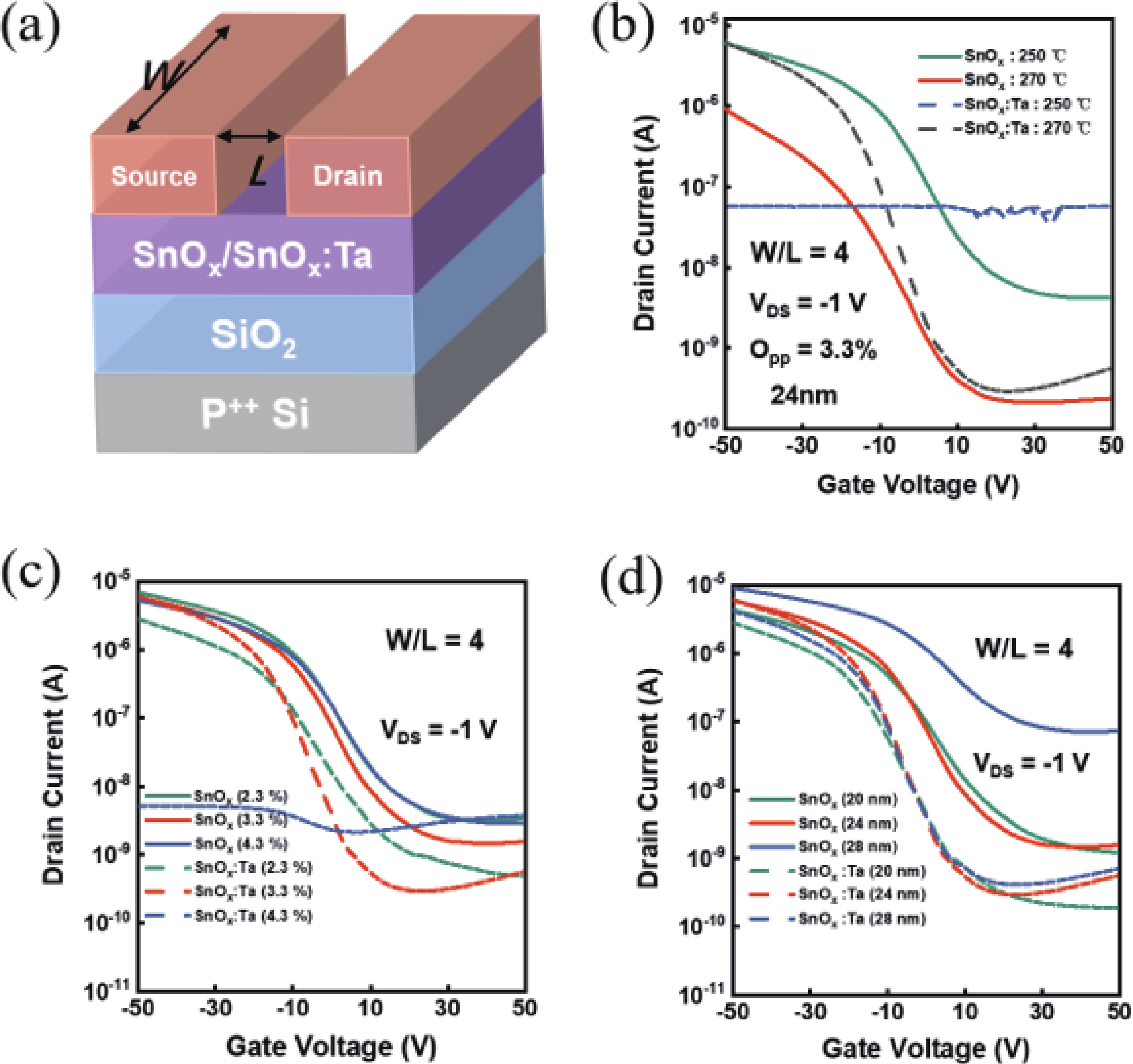
In this work, the incorporation of tantalum (Ta) into p-type metal-oxide (SnOx) semiconductor film is investigated to improve the electrical characteristics and suppress the fringe effect of thin film transistors (TFTs). The Ta-doped SnOx (SnOx:Ta) film is deposited by radio-frequency (RF) magnetron sputtering with a Sn:Ta (3at.%) target and thermally annealed at 270 °C for 30 min. Here, we observe that the SnOx:Ta film presents increased crystallinity, reduced defect density (3.25 × 1012 cm−2·eV−1), and widened bandgap (1.98 eV), in comparison with the undoped SnOx film. As a result, the SnOx:Ta TFTs exhibit a lower off-state current (Ioff), an improved on/off current ratio (2.17 × 10⁴), a remarkably decreased subthreshold swing (SS) by 41%, and enhanced device stability. Additionally, by introducing Ta dopants, the fringe effect as well as the impact of channel width-to-length ratio (W/L) on electrical performances of the p-type oxide TFTs can be effectively suppressed. These results shall contribute to further exploration and development of p-type SnOx TFTs.


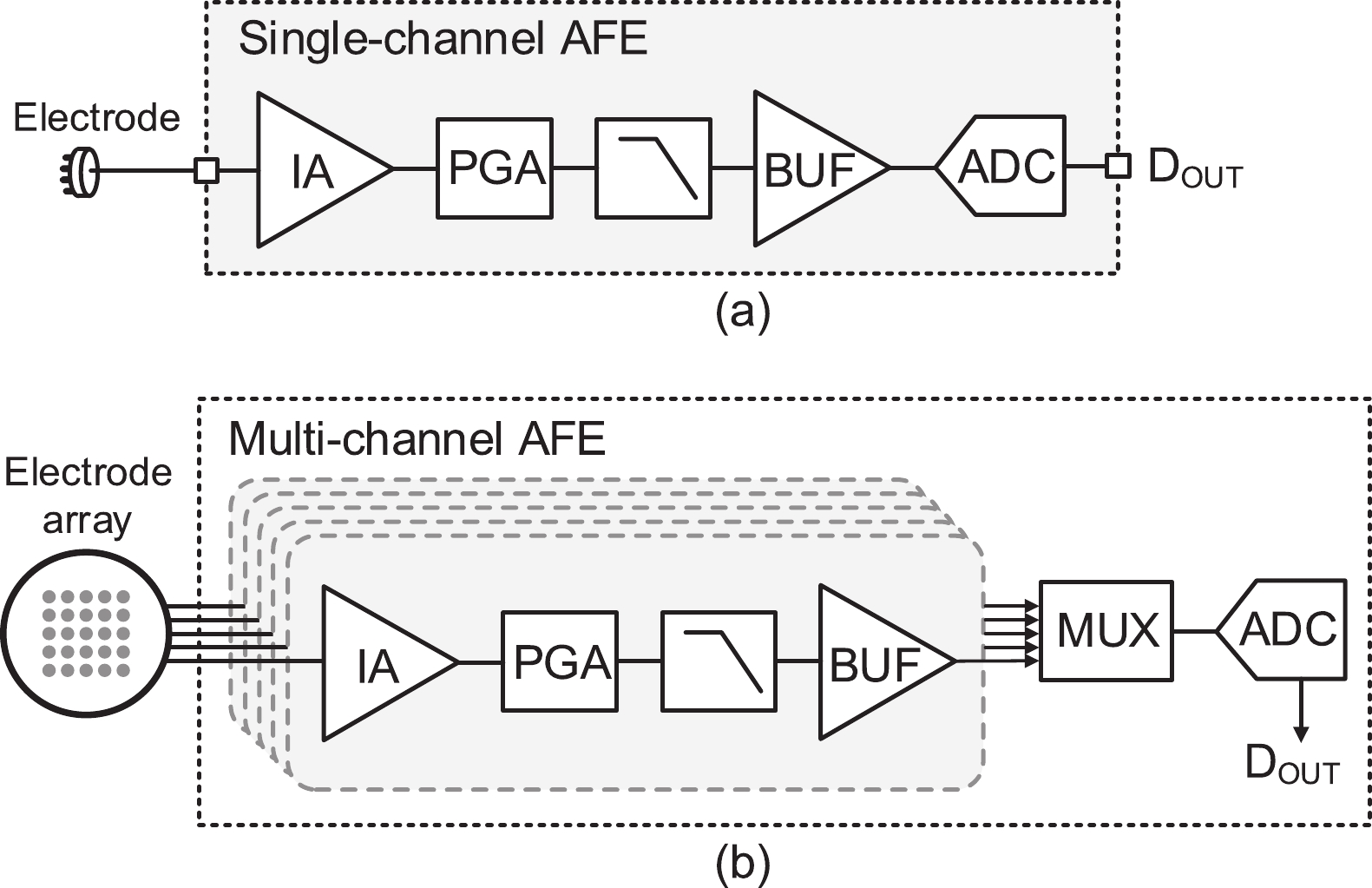
This paper presents the design of a low-power multi-channel analog front-end (AFE) for bio-potential recording. By using time division multiplexing (TDM), a successive approximation register analog-to-digital converter (SAR ADC) is shared among all 20 channels. A charge-sharing multiplexer (MUX) is proposed to transmit the output signals from the respective channels to the ADC. By separately pre sampling the output of each channel, the sampling time of each channel is greatly extended and additional active buffers are avoided. The AFE is fabricated in a 65-nm CMOS process, and the whole system consumes 28.2 μW under 1 V supply. Each analog acquisition channel consumes 1.25 μW and occupies a chip area of 0.14 mm2. Measurement results show that the AFE achieves an input referred noise of 1.8 μV∙rms in a 350 Hz bandwidth and a noise efficiency factor (NEF) of 4.1. The 12-bit SAR ADC achieves an ENOB of 9.8 bit operating at 25 kS/s. The AFE is experimented on real-world applications by measuring human ECG and a clear ECG waveform is captured.


Robotic computing systems play an important role in enabling intelligent robotic tasks through intelligent algorithms and supporting hardware. In recent years, the evolution of robotic algorithms indicates a roadmap from traditional robotics to hierarchical and end-to-end models. This algorithmic advancement poses a critical challenge in achieving balanced system-wide performance. Therefore, algorithm-hardware co-design has emerged as the primary methodology, which analyzes algorithm behaviors on hardware to identify common computational properties. These properties can motivate algorithm optimization to reduce computational complexity and hardware innovation from architecture to circuit for high performance and high energy efficiency. We then reviewed recent works on robotic and embodied AI algorithms and computing hardware to demonstrate this algorithm-hardware co-design methodology. In the end, we discuss future research opportunities by answering two questions: (1) how to adapt the computing platforms to the rapid evolution of embodied AI algorithms, and (2) how to transform the potential of emerging hardware innovations into end-to-end inference improvements.


A silicon-based germanium (Ge) photodetector working for C and L bands is proposed in this paper. The device features a novel asymmetric PIN structure, which contributes to a more optimized electric field distribution in Ge and a shorter effective width of depleted region. Meanwhile, the optical structure is designed carefully to enhance responsivity for broadband. Under −7 V, where the weak avalanche process happens, the responsivity of our device is 1.49 and 1.16 A/W at 1550 and 1600 nm, with bandwidth of 47.1 and 44.5 GHz, respectively. These performances demonstrate the significant application potential of the device in optical communication systems.


GaN diodes for high energy (64.8 MeV) proton detection were fabricated and investigated. A comparison of the performance of GaN diodes with different structures is presented, with a focus on sapphire and on GaN substrates, Schottky and pin diodes, and different active layer thicknesses. Pin diodes fabricated on a sapphire substrate are the best choice for a GaN proton detector working at 0 V bias. They are sensitive (minimum detectable proton beam <1 pA/cm2), linear as a function of proton current and fast (<1 s). High proton current sensitivity and high spatial resolution of GaN diodes can be exploited in the future for proton imaging of patients in proton therapy.


This paper presents a 4-level pulse amplitude modulation (PAM-4) distributed feedback (DFB) laser driver. The driver adopts a digital slicing architecture to achieve high linearity by adjusting the weights of three thermometer-coded main paths. An efficient-biased output stage structure is proposed to reduce power consumption while avoiding the degradation of output node bandwidth typically induced by parasitic capacitance in high-current bias path. A two-tap linear and nonlinear feed-forward equalizer (FFE) is implemented in the digital domain to extend bandwidth limitations and compensate for the dynamic nonlinearity of the DFB laser. The nonlinear FFE is realized at the cost of lower power consumption and smaller area by utilizing the simultaneity of low-speed parallel data. The chip is fabricated in 28 nm CMOS process. Measurement results indicate that, with a laser bias current of 40 mA, a modulation current of 20 mApp, and an operating rate of 32 Gb/s PAM-4, the overall power consumption of the chip is 372 mW, corresponding to an energy efficiency of 11.6 pJ/b.


All-inorganic CsPbBr3 perovskite quantum dots (QDs) have attracted extensive attention in photoelectric detection for their excellent photoelectric properties and stability. However, the CsPbBr3 quantum dot film exhibits a high non-radiative recombination rate, and the mismatch in energy levels with the carbon electrode weakens hole extraction efficiency. These reduces the device's performance. To improve this, a semiconductor photodetector based on fluorine-doped tin oxide (FTO)/dense titanium dioxide (c-TiO2)/mesoporous titanium dioxide (m-TiO2)/CsPbBr3 QDs/CsPbBrxI3–x (x = 2, 1.5, 1) QDs/C structure was studied. By adjusting the Br– : I– ratio, the synthesized CsPbBrxI3–x (x = 2, 1.5, 1) QDs showed an adjustable band gap width of 2.284−2.394 eV. And forming a type Ⅱ band structure with CsPbBr3 QDs, which reduced the valence band offset between the active layer and the carbon electrode, this promoted carrier extraction and reduced non-radiative recombination rate. Compared with the original device (the photosensitive layer is CsPbBr3 QDs), the performance of the photodetector based on the CsPbBr3 QDs/CsPbBr2I QDs heterostructure is significantly improved, the responsivity (R) increased by 73%, the specific detectivity rate (D*) increased from 6.98 × 10¹² to 3.19 × 10¹³ Jones, the on/off ratio reached 106. This study provides a new idea for the development of semiconductor tandem detectors.


Accurate quantification of exercise interventions and changes in muscle function is essential for personalized health management. Electrical impedance myography (EIM) technology offers an innovative, noninvasive, painless, and easy-to-perform solution for muscle health monitoring. However, current EIM platforms face a number of limitations, including large device size, wired connections, and instability of the electrode-skin interface, which limit their applicability for monitoring muscle movement. In this study, a miniature wireless EIM platform with a user-friendly smartphone app is proposed and developed. The miniature, wireless, multi-frequency (20 kHz−1 MHz) EIM platform is equipped with flexible microneedle array electrodes (MAE). The advantages of MAEs over conventional electrodes were demonstrated by physical field modeling simulations and skin-electrode contact impedance comparison tests. The smartphone APP was developed to wirelessly operate the EIM platform, and to transmit and process real-time muscle impedance data. To validate its effectiveness, a seven-day adaptive fatigue training study was conducted, which demonstrated that the EIM platform was able to detect muscle adaptations and serve as a reliable indicator of fatigue. This study presents an innovative approach to applying EIM technology to muscle health monitoring and exercise testing, thereby advancing the development of personalized health management and athletic performance assessment.


The dynamic avalanche effect is a critical factor influencing the performance and reliability of the field-stop insulated gate bipolar transistors (FS-IGBT). Unclamped inductive switching (UIS) is the primary method for testing the dynamic avalanche capability of FS-IGBTs. Numerous studies have demonstrated that factors such as device structure, avalanche-generating current filaments, and electrical parameters influence the dynamic avalanche effect of the FS-IGBT. However, few studies have focused on enhancing the avalanche reliability of the FS-IGBT by adjusting circuit parameters during operation. In this paper, the dynamic avalanche effect of the FS-IGBT under UIS conditions is comprehensively investigated through a series of comparative experiments with varying circuit parameters, including bus voltage VDC, gate voltage VG, gate resistance Rg, load inductance L, and temperature TC. Furthermore, a method to enhance the dynamic avalanche reliability of the FS-IGBT under UIS by optimizing circuit parameters is proposed. In practical applications, reducing gate voltage, increasing load inductance, and lowering temperature can effectively improve the dynamic avalanche capability of the FS-IGBT.


This paper describes a 2D/3D vision chip with integrated sensing and processing capabilities. The 2D/3D vision chip architecture includes a 2D/3D image sensor and a programmable visual processor. In this architecture, we design a novel on-chip processing flow with die-to-die image transmission and low-latency fixed-point image processing. The vision chip achieves real-time end-to-end processing of convolutional neural networks (CNNs) and conventional image processing algorithms. Furthermore, an end-to-end 2D/3D vision system is built to exhibit the capacity of the vision chip. The vision system achieves real-timing applications under 2D and 3D scenes, such as human face detection (processing delay 10.2 ms) and depth map reconstruction (processing delay 4.1 ms). The frame rate of image acquisition, image process, and result display is larger than 30 fps.


Low power consumption, high responsivity, and self-powering are key objectives for photoelectrochemical ultraviolet detectors. In this research, In-doped α-Ga2O3 nanowire arrays were fabricated on FTO substrates through a hydrothermal approach, with subsequent thermal annealing. These arrays were then used as photoanodes to construct a ultraviolet (UV) photodetector. In doping reduced the bandgap of α-Ga2O3, enhancing its absorption of UV light. Consequently, the In-doped α-Ga2O3 nanowire arrays exhibited excellent light detection performance. When irradiated by 255 nm deep ultraviolet light, they obtained a responsivity of 38.85 mA/W. Moreover, the detector's response and recovery times are 13 and 8 ms, respectively. The In-doped α-Ga2O3 nanowire arrays exhibit a responsivity that is about three-fold higher than the undoped one. Due to its superior responsivity, the In-doped device was used to develop a photoelectric imaging system. This study demonstrates that doping α-Ga2O3 nanowire with indium is a potent approach for optimizing their photoelectrochemical performance, which also has significant potential for optoelectronic applications.


In this work, we design and fabricate AlGaN/GaN-based Schottky barrier diodes (SBDs) on a silicon substrate with a trenched n+-GaN cap layer. With the developed physical models, we find that the n+-GaN cap layer provides more electrons into the AlGaN/GaN channel, which is further confirmed experimentally. When compared with the reference device, this increases the two-dimensional electron gas (2DEG) density by two times and leads to a reduced specific ON-resistance (Ron,sp) of ~2.4 mΩ·cm2. We also adopt the trenched n+-GaN structure such that partial of the n+-GaN is removed by using dry etching process to eliminate the surface electrical conduction when the device is set in the off-state. To suppress the surface defects that are caused by the dry etching process, we also deposit Si3N4 layer prior to the deposition of field plate (FP), and we obtain a reduced leakage current of ~8 × 10⁻⁵ A·cm−2 and breakdown voltage (BV) of 876 V. The Baliga’s figure of merit (BFOM) for the proposed structure is increased to ~319 MW·cm−2. Our investigations also find that the pre-deposited Si3N4 layer helps suppress the electron capture and transport processes, which enables the reduced dynamic Ron,sp.


AlGaN-based LEDs with peak wavelength below 240 nm (far-UVC) pose no significant harm to human health, thus highlighting their broader application potential. While, there is a significant Schottky barrier between the n-electrode and Al-rich n-AlGaN, adversely impeding electron injection and resulting in considerable heat generation. Here, we fabricate V-based electrodes of V/Al/Ti/Au on n-AlGaN with Al content over 80% and investigate the relationship between the metal diffusion and contact properties during the high-temperature annealing process. Experiments reveal that decreasing V thickness in the electrode promotes the diffusion of Al towards the surface of n-AlGaN, which facilitates the formation of VN and thus the increase of local electron concentration, resulting in lower specific contact resistivity. Then, increasing the Al thickness inhibits the diffusion of Au to the n-AlGaN surface, suppressing the rise of Schottky barrier. Experimentally, an optimized n-electrode of V(10 nm)/Al(240 nm)/Ti(40 nm)/Au(50 nm) on n-Al0.81Ga0.19N is obtained, realizing an optimal specific contact resistivity of 7.30 × 10⁻⁴ Ω·cm2. Based on the optimal n-electrode preparation scheme for Al-rich n-AlGaN, the work voltage of a far-UVC LED with peak wavelength of 233.5 nm is effectively reduced.


The event-based vision sensor (EVS), which can generate efficient spiking data streams by exclusively detecting motion, exemplifies neuromorphic vision methodologies. Generally, its inherent lack of texture features limits effectiveness in complex vision processing tasks, necessitating supplementary visual information. However, to date, no event-based hybrid vision solution has been developed that preserves the characteristics of complete spike data streams to support synchronous computation architectures based on spiking neural network (SNN). In this paper, we present a novel spike-based sensor with digitized pixels, which integrates the event detection structure with the pulse frequency modulation (PFM) circuit. This design enables the simultaneous output of spiking data that encodes both temporal changes and texture information. Fabricated in 180 nm process, the proposed sensor achieves a resolution of 128 × 128, a maximum event rate of 960 Meps, a grayscale framerate of 117.1 kfps, and a measured power consumption of 60.1 mW, which is suited for high-speed, low-latency, edge SNN-based vision computing systems.


Doping plays a pivotal role in enhancing the performance of organic semiconductors (OSCs) for advanced optoelectronic and thermoelectric applications. In this study, we systematically investigated the doping performance and applicability of the ionic dopant 4-isopropyl-4′-methyldiphenyliodonium tetrakis(penta-fluorophenyl-borate) (DPI-TPFB) as a p-dopant for OSCs. Using the p-type OSC PBBT-2T as a model system, we demonstrated that DPI-TPFB shows significant doping effect, as confirmed by ESR spectra, UV−vis−NIR absorption, and work function analysis, and enhances the electronic conductivity of PBBT-2T films by over four orders of magnitude. Furthermore, DPI-TPFB exhibited broad doping applicability, effectively doping various p-type OSCs and even imparting p-type characteristics to the n-type OSC N2200, transforming its intrinsic n-type behavior into p-type. The application of DPI-TPFB-doped PBBT-2T films in organic thermoelectric devices (OTEs) was also explored, achieving a power factor of approximately 10 μW∙m−1∙K−2. These findings highlight the potential of DPI-TPFB as a versatile and efficient dopant for integration into organic optoelectronic and thermoelectric devices.


Thermally chargeable supercapacitors (TCSCs) have unique advantages in the collection, conversion, and storage of thermal energy, contributing to the development of new strategies for thermal energy utilization. 2D MXene materials are predicted to be highly promising new thermoelectric materials. Here, we report a self-assembled flexible Ti3C2Tx MXene-based TCSC device, using prepared Ti3C2Tx MXene as the capacitor electrode and a NaClO4/PEO gel as the electrolyte. We also explore the working mechanism of the TCSCs. The fabricated Ti3C2Tx-based TCSCs exhibit an excellent Seebeck coefficient of 11.8 mV∙K−1 on average and maintain good cycling stability under various temperature differences. Demonstrations of multiple practical applications show that Ti3C2Tx MXene-based TCSC devices are excellent candidates for self-powered integrated electronic devices.


Silicon carbide offers distinct advantages in the field of power electronic devices. However, manufacturing processes remain a significant barrier to its widespread adoption. Polycrystalline SiC is less expensive and easier to produce than single crystal. But stabilizing and controlling its performance are critical challenges that must be addressed urgently. Due to its material properties and excellent performance in applications, 3C-SiC is gaining increasing attention in research. This article presents the electrical and material properties of a series of polycrystalline 3C-SiC samples and investigates their interrelationship. The samples were examined using TEM, which confirmed their polycrystalline structure. Combined with XRD and Raman spectroscopy, the grain orientations within the samples were analyzed, and the presence of stress was verified. EBSD was employed to statistically examine the grain structure and size across samples. For samples with similar doping levels, grain size is the most influential factor in determining electrical characteristics. Further EBSD measurements reveal the relationship between resistivity and grain size as log(ρ) = −1.93 + 8.67/d. These findings provide a foundation for the quantitative control and application of polycrystalline 3C-SiC. This work offers theoretical evidence for optimizing the performance tuning of 3C-SiC ceramics and enhancing their effectiveness in electronic applications.


