


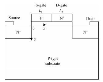
Fig. 1.
Cross-sectional view of the SMDWG MOSFET
SEMICONDUCTOR DEVICES
Changyong Zheng1, 2, , Wei Zhang1, Tailong Xu1, Yuehua Dai1 and Junning Chen1
Corresponding author: Zheng Changyong, Email:zhengcy_628@163.com
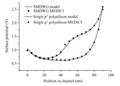
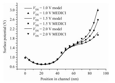
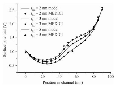
Abstract: An analytical surface potential model for the single material double work function gate (SMDWG) MOSFET is developed based on the exact resultant solution of the two-dimensional Poisson equation. The model includes the effects of drain biases, gate oxide thickness, different combinations of S-gate and D-gate length and values of substrate doping concentration. More attention has been paid to seeking to explain the attributes of the SMDWG MOSFET, such as suppressing drain-induced barrier lowering (DIBL), accelerating carrier drift velocity and device speed. The model is verified by comparison to the simulated results using the device simulator MEDICI. The accuracy of the results obtained using our analytical model is verified using numerical simulations. The model not only offers the physical insight into device physics but also provides the basic designing guideline for the device.
Key words: analytical model, surface potential, single material double work function gate (SMDWG) MOSFET, simulation, DIBL
| [1] |
Dennard R H, Gaensslen F H, Yu H N, et al. Design of ion-implanted MOSFET's with very small physical dimensions. IEEE J Solid-State Circuits, 1974, SC-9:256
|
| [2] |
Cappy A, Carres B, Fanquembergues R, et al. Comparative potential performance of Si, GaAs, GaInAs, InAs submicrometer-gate FET's. IEEE Trans Electron Devices, 1980, ED-27:2158
|
| [3] |
Long W, Ou H, Kuo J M, et al. Dual material gate (DMG) field-effect transistor. IEEE Trans Electron Devices, 1999, 46:865 doi: 10.1109/16.760391
|
| [4] |
Saxena M, Haldar S, Gupta M, et al. Physics-based analytical modeling of potential and electrical field distribution in dual material gate (DMG)-MOSFET for improved hot electron effect and carrier transport efficiency. IEEE Trans Electron Devices, 2002, 49:1928 doi: 10.1109/TED.2002.804701
|
| [5] |
Kumar M J, Chaudhry A. Two-dimensional analytical modeling of fully depleted DMG SOI MOSFET and evidence for diminished SCEs. IEEE Trans Electron Devices, 2004, 51:569 doi: 10.1109/TED.2004.823803
|
| [6] |
Chiang T K. A new two-dimensional analytical subthreshold behavior model for short-channel tri-material gate-stack SOI MOSFET's. Microelectron Reliab, 2009, 49:113 doi: 10.1016/j.microrel.2008.11.005
|
| [7] |
Saxena R S, Kumar M J. Dual-material-gate technique for enhanced transconductance and breakdown voltage of trench power MOSFETs. IEEE Trans Electron Devices, 2009, 56:517 doi: 10.1109/TED.2008.2011723
|
| [8] |
Chiang T K. A new compact subthreshold behavior model for dual-material surrounding gate (DMSG) MOSFETs. Solid-State Electron, 2009, 53:490 doi: 10.1016/j.sse.2009.02.007
|
| [9] |
Sharma R K, Gupta R, Gupta M, et al. Dual-material double-gate SOI n-MOSFET:gate misalignment analysis. IEEE Trans Electron Devices, 2009, 56:1284 doi: 10.1109/TED.2009.2019695
|
| [10] |
Saurabh S, Kumar M J. Novel attributes of a dual material gate nanoscale tunnel field-effect transistor. IEEE Trans Electron Devices, 2011, 58:404 doi: 10.1109/TED.2010.2093142
|
| [11] |
Li Zunchao, Jiang Yaolin, Wu Jianmin. Dual material gate SOI MOSFET with a single halo. Chinese Journal of Semiconductors, 2007, 28:327
|
| [12] |
Luan Suzhen, Liu Hongxia, Jia Renxu, et al. A two-dimensional subthreshold current model for dual material gate SOI nMOSFETs with asymmetric halo. Journal of Semiconductors, 2008, 29:746 http://www.jos.ac.cn/bdtxben/ch/reader/view_abstract.aspx?flag=1&file_no=07091301&journal_id=bdtxbcn
|
| [13] |
Li Jin, Liu Hongxia, Li Bin, et al. Two-dimensional threshold voltage analytical model of DMG strained-silicon-on-insulator MOSFETs. Journal of Semiconductors, 2010, 31:084008 doi: 10.1088/1674-4926/31/8/084008
|
| [14] |
Li Jin, Liu Hongxia, Yuan Bo, et al. A two-dimensional analytical model of fully depleted asymmetrical dual material gate double-gate strained-Si MOSFETs. Journal of Semiconductors, 2011, 32:044005 doi: 10.1088/1674-4926/32/4/044005
|
| [15] |
Cao Lei, Liu Hongxia, Wang Guanyu. Study of modeling for hetero-material gate fully depleted SSDOIMOSFET. Acta Phys Sin, 2012, 61:017105
|
| [16] |
Polihchuk I, Ranade P, King T J, et al. Dual work function metal gate CMOS technology using metal inter-diffusion. IEEE Electron Device Lett, 2001, 22:444 doi: 10.1109/55.944334
|
| [17] |
Young K K. Short-channel effect in fully depleted SOI MOSFETs. IEEE Trans Electron Devices, 1989, 36:399 doi: 10.1109/16.19942
|
| [18] |
Suzuki K. Short-channel MOSFET using a universal channel depletion width parameter. IEEE Trans Electron Devices, 2000, 47:1202 doi: 10.1109/16.842962
|


Article views: 3125 Times PDF downloads: 17 Times Cited by: 0 Times
Received: 04 February 2013 Revised: 07 March 2013 Online: Published: 01 September 2013
| Citation: |
Changyong Zheng, Wei Zhang, Tailong Xu, Yuehua Dai, Junning Chen. A compact model for single material double work function gate MOSFET[J]. Journal of Semiconductors, 2013, 34(9): 094006. doi: 10.1088/1674-4926/34/9/094006
****
C Y Zheng, W Zhang, T L Xu, Y H Dai, J N Chen. A compact model for single material double work function gate MOSFET[J]. J. Semicond., 2013, 34(9): 094006. doi: 10.1088/1674-4926/34/9/094006.

|
| [1] |
Dennard R H, Gaensslen F H, Yu H N, et al. Design of ion-implanted MOSFET's with very small physical dimensions. IEEE J Solid-State Circuits, 1974, SC-9:256
|
| [2] |
Cappy A, Carres B, Fanquembergues R, et al. Comparative potential performance of Si, GaAs, GaInAs, InAs submicrometer-gate FET's. IEEE Trans Electron Devices, 1980, ED-27:2158
|
| [3] |
Long W, Ou H, Kuo J M, et al. Dual material gate (DMG) field-effect transistor. IEEE Trans Electron Devices, 1999, 46:865 doi: 10.1109/16.760391
|
| [4] |
Saxena M, Haldar S, Gupta M, et al. Physics-based analytical modeling of potential and electrical field distribution in dual material gate (DMG)-MOSFET for improved hot electron effect and carrier transport efficiency. IEEE Trans Electron Devices, 2002, 49:1928 doi: 10.1109/TED.2002.804701
|
| [5] |
Kumar M J, Chaudhry A. Two-dimensional analytical modeling of fully depleted DMG SOI MOSFET and evidence for diminished SCEs. IEEE Trans Electron Devices, 2004, 51:569 doi: 10.1109/TED.2004.823803
|
| [6] |
Chiang T K. A new two-dimensional analytical subthreshold behavior model for short-channel tri-material gate-stack SOI MOSFET's. Microelectron Reliab, 2009, 49:113 doi: 10.1016/j.microrel.2008.11.005
|
| [7] |
Saxena R S, Kumar M J. Dual-material-gate technique for enhanced transconductance and breakdown voltage of trench power MOSFETs. IEEE Trans Electron Devices, 2009, 56:517 doi: 10.1109/TED.2008.2011723
|
| [8] |
Chiang T K. A new compact subthreshold behavior model for dual-material surrounding gate (DMSG) MOSFETs. Solid-State Electron, 2009, 53:490 doi: 10.1016/j.sse.2009.02.007
|
| [9] |
Sharma R K, Gupta R, Gupta M, et al. Dual-material double-gate SOI n-MOSFET:gate misalignment analysis. IEEE Trans Electron Devices, 2009, 56:1284 doi: 10.1109/TED.2009.2019695
|
| [10] |
Saurabh S, Kumar M J. Novel attributes of a dual material gate nanoscale tunnel field-effect transistor. IEEE Trans Electron Devices, 2011, 58:404 doi: 10.1109/TED.2010.2093142
|
| [11] |
Li Zunchao, Jiang Yaolin, Wu Jianmin. Dual material gate SOI MOSFET with a single halo. Chinese Journal of Semiconductors, 2007, 28:327
|
| [12] |
Luan Suzhen, Liu Hongxia, Jia Renxu, et al. A two-dimensional subthreshold current model for dual material gate SOI nMOSFETs with asymmetric halo. Journal of Semiconductors, 2008, 29:746 http://www.jos.ac.cn/bdtxben/ch/reader/view_abstract.aspx?flag=1&file_no=07091301&journal_id=bdtxbcn
|
| [13] |
Li Jin, Liu Hongxia, Li Bin, et al. Two-dimensional threshold voltage analytical model of DMG strained-silicon-on-insulator MOSFETs. Journal of Semiconductors, 2010, 31:084008 doi: 10.1088/1674-4926/31/8/084008
|
| [14] |
Li Jin, Liu Hongxia, Yuan Bo, et al. A two-dimensional analytical model of fully depleted asymmetrical dual material gate double-gate strained-Si MOSFETs. Journal of Semiconductors, 2011, 32:044005 doi: 10.1088/1674-4926/32/4/044005
|
| [15] |
Cao Lei, Liu Hongxia, Wang Guanyu. Study of modeling for hetero-material gate fully depleted SSDOIMOSFET. Acta Phys Sin, 2012, 61:017105
|
| [16] |
Polihchuk I, Ranade P, King T J, et al. Dual work function metal gate CMOS technology using metal inter-diffusion. IEEE Electron Device Lett, 2001, 22:444 doi: 10.1109/55.944334
|
| [17] |
Young K K. Short-channel effect in fully depleted SOI MOSFETs. IEEE Trans Electron Devices, 1989, 36:399 doi: 10.1109/16.19942
|
| [18] |
Suzuki K. Short-channel MOSFET using a universal channel depletion width parameter. IEEE Trans Electron Devices, 2000, 47:1202 doi: 10.1109/16.842962
|

 WeChat ID
Journal of Semiconductors © 2017 All Rights Reserved 京ICP备05085259号-2

 DownLoad:

